EP0337331B1 - Procédé pour fabriquer une ligne de transmission blindée de tous côtés - Google Patents
Procédé pour fabriquer une ligne de transmission blindée de tous côtés Download PDFInfo
- Publication number
- EP0337331B1 EP0337331B1 EP19890106223 EP89106223A EP0337331B1 EP 0337331 B1 EP0337331 B1 EP 0337331B1 EP 19890106223 EP19890106223 EP 19890106223 EP 89106223 A EP89106223 A EP 89106223A EP 0337331 B1 EP0337331 B1 EP 0337331B1
- Authority
- EP
- European Patent Office
- Prior art keywords
- thereafter
- copper
- film
- areas
- conductive layer
- Prior art date
- Legal status (The legal status is an assumption and is not a legal conclusion. Google has not performed a legal analysis and makes no representation as to the accuracy of the status listed.)
- Expired - Lifetime
Links
Images
Classifications
-
- H—ELECTRICITY
- H05—ELECTRIC TECHNIQUES NOT OTHERWISE PROVIDED FOR
- H05K—PRINTED CIRCUITS; CASINGS OR CONSTRUCTIONAL DETAILS OF ELECTRIC APPARATUS; MANUFACTURE OF ASSEMBLAGES OF ELECTRICAL COMPONENTS
- H05K1/00—Printed circuits
- H05K1/02—Details
- H05K1/0213—Electrical arrangements not otherwise provided for
- H05K1/0216—Reduction of cross-talk, noise or electromagnetic interference
- H05K1/0218—Reduction of cross-talk, noise or electromagnetic interference by printed shielding conductors, ground planes or power plane
- H05K1/0219—Printed shielding conductors for shielding around or between signal conductors, e.g. coplanar or coaxial printed shielding conductors
- H05K1/0221—Coaxially shielded signal lines comprising a continuous shielding layer partially or wholly surrounding the signal lines
-
- H—ELECTRICITY
- H01—ELECTRIC ELEMENTS
- H01P—WAVEGUIDES; RESONATORS, LINES, OR OTHER DEVICES OF THE WAVEGUIDE TYPE
- H01P11/00—Apparatus or processes specially adapted for manufacturing waveguides or resonators, lines, or other devices of the waveguide type
- H01P11/001—Manufacturing waveguides or transmission lines of the waveguide type
-
- H—ELECTRICITY
- H01—ELECTRIC ELEMENTS
- H01P—WAVEGUIDES; RESONATORS, LINES, OR OTHER DEVICES OF THE WAVEGUIDE TYPE
- H01P3/00—Waveguides; Transmission lines of the waveguide type
- H01P3/02—Waveguides; Transmission lines of the waveguide type with two longitudinal conductors
- H01P3/06—Coaxial lines
-
- H—ELECTRICITY
- H05—ELECTRIC TECHNIQUES NOT OTHERWISE PROVIDED FOR
- H05K—PRINTED CIRCUITS; CASINGS OR CONSTRUCTIONAL DETAILS OF ELECTRIC APPARATUS; MANUFACTURE OF ASSEMBLAGES OF ELECTRICAL COMPONENTS
- H05K3/00—Apparatus or processes for manufacturing printed circuits
- H05K3/46—Manufacturing multilayer circuits
- H05K3/4644—Manufacturing multilayer circuits by building the multilayer layer by layer, i.e. build-up multilayer circuits
- H05K3/465—Manufacturing multilayer circuits by building the multilayer layer by layer, i.e. build-up multilayer circuits by applying an insulating layer having channels for the next circuit layer
-
- H—ELECTRICITY
- H05—ELECTRIC TECHNIQUES NOT OTHERWISE PROVIDED FOR
- H05K—PRINTED CIRCUITS; CASINGS OR CONSTRUCTIONAL DETAILS OF ELECTRIC APPARATUS; MANUFACTURE OF ASSEMBLAGES OF ELECTRICAL COMPONENTS
- H05K2201/00—Indexing scheme relating to printed circuits covered by H05K1/00
- H05K2201/07—Electric details
- H05K2201/0707—Shielding
- H05K2201/0715—Shielding provided by an outer layer of PCB
-
- H—ELECTRICITY
- H05—ELECTRIC TECHNIQUES NOT OTHERWISE PROVIDED FOR
- H05K—PRINTED CIRCUITS; CASINGS OR CONSTRUCTIONAL DETAILS OF ELECTRIC APPARATUS; MANUFACTURE OF ASSEMBLAGES OF ELECTRICAL COMPONENTS
- H05K2203/00—Indexing scheme relating to apparatus or processes for manufacturing printed circuits covered by H05K3/00
- H05K2203/07—Treatments involving liquids, e.g. plating, rinsing
- H05K2203/0703—Plating
- H05K2203/0733—Method for plating stud vias, i.e. massive vias formed by plating the bottom of a hole without plating on the walls
-
- H—ELECTRICITY
- H05—ELECTRIC TECHNIQUES NOT OTHERWISE PROVIDED FOR
- H05K—PRINTED CIRCUITS; CASINGS OR CONSTRUCTIONAL DETAILS OF ELECTRIC APPARATUS; MANUFACTURE OF ASSEMBLAGES OF ELECTRICAL COMPONENTS
- H05K3/00—Apparatus or processes for manufacturing printed circuits
- H05K3/0011—Working of insulating substrates or insulating layers
- H05K3/0017—Etching of the substrate by chemical or physical means
- H05K3/0023—Etching of the substrate by chemical or physical means by exposure and development of a photosensitive insulating layer
-
- H—ELECTRICITY
- H05—ELECTRIC TECHNIQUES NOT OTHERWISE PROVIDED FOR
- H05K—PRINTED CIRCUITS; CASINGS OR CONSTRUCTIONAL DETAILS OF ELECTRIC APPARATUS; MANUFACTURE OF ASSEMBLAGES OF ELECTRICAL COMPONENTS
- H05K3/00—Apparatus or processes for manufacturing printed circuits
- H05K3/10—Apparatus or processes for manufacturing printed circuits in which conductive material is applied to the insulating support in such a manner as to form the desired conductive pattern
- H05K3/108—Apparatus or processes for manufacturing printed circuits in which conductive material is applied to the insulating support in such a manner as to form the desired conductive pattern by semi-additive methods; masks therefor
Definitions
- the invention relates to a method for producing a signal line shielded on all sides for high-frequency circuits.
- signal lines shielded on all sides are e.g. Coaxial lines with a rectangular cross section or symmetrical triplate lines shielded on all sides, as are used for connecting high and ultra-high frequency circuits, in particular in integrated microwave circuits.
- a known method for producing shielded signal lines in semiconductor radio-frequency circuits has, in addition to other method steps, essentially steps a), b) and c) of the method according to claim 1 on.
- a prepreg film is laminated there under the action of pressure and heat. That which then covers the conductor tracks Insulating material is removed mechanically. Such mechanical processing is difficult to carry out and requires a lot of effort.
- the invention has for its object to provide a simple and reliable method for producing all-sided shielded signal lines in high and ultra-high frequency circuits that effectively prevent crosstalk.
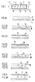
- Two signal lines 1 and 2 manufactured according to the invention are part of a high-frequency circuit 3 shown in the drawing (FIG. 1) only in section, and the signal lines 1 and 2 are designed as rectangular coaxial lines, which are arranged on a common carrier 4.
- the carrier 4 is e.g. made from a glass fiber reinforced epoxy resin.
- the signal lines 1, 2 each have an inner conductor 6 and an outer conductor or an outer shield wall 7.
- the inner conductor 6 and the outer conductor 7 are made of a highly conductive material, e.g. made on copper.
- the inner cavities 8 of the signal lines 1, 2 and the spaces 9 between the signal lines 1 and 2 and other circuit components are filled with a dielectric which is made of a photostructurable material, e.g. consists of epoxy or polyimide. These areas filled with dielectric will, as will be explained with reference to Fig. 2, with permanent resist films, e.g. made from a solder resist with final hardening.
- a photostructurable material e.g. consists of epoxy or polyimide.
- FIG. 2 The individual steps of the method according to the invention are shown schematically in FIG. 2, progressively from top to bottom. They are designated in the drawing with the letters A to M, which correspond to process steps a) to m) of claim 1. These letters therefore denote the successive process steps, but not or only indirectly the individual material layers.
- a photostructurable film 11 is laminated onto a carrier material 10 clad or metallized with copper.
- the carrier 4 consists, for example, of the glass-fiber reinforced plastic known under the name FR4, the photostructurable film 11 consists of a permanent resist, for example a solder resist film with final hardening.
- the photostructurable film 11 is subjected to a photoprocess which consists in a known manner of exposing the areas to be left and subsequently developing it. Areas 12 which correspond to the position of the outer conductor 7 of the finished signal line 1 or 2 are removed.
- the removed areas 12 are filled with copper by electrodeposition.
- a thin conductive layer 14 is applied to the outer surface of the remaining areas of the film 11 and the outer conductor areas 12 filled with copper by chemical deposition of copper. This conductive layer 14 is electrically conductively connected to the copper layer 10 via the region 12.
- a photoresist film 15 is applied to the conductive layer 14 and regions 16 which correspond to the position of the inner conductor 6 of the signal lines 1 or 2 are removed from this by a new photoprocess.
- the regions 16 are brought to the strength required for a signal conductor by electrodeposition of copper.
- the remaining areas of the photoresist film are stripped, ie chemically dissolved.
- the conductive layer 14 exposed by stripping the photoresist film 15 is removed by a copper differential etching.
- the lower half of the outer conductor 7 is made and the inner conductor 6 from the other conductive areas, i.e. from the outer conductor 7, galvanically isolated.
- Another photostructurable film 18 is laminated onto the exposed surface. This is indicated in the drawing by a dashed line.
- This film 18 also consists of a permanent resist, e.g. a solder resist in foil form.
- the film 18 is removed in areas 19 which correspond to the upper part of the outer conductor 7 by a further photo process.
- the removed areas 19 are filled with copper by electrodeposition.
- a thin conductive layer 20 is applied to the free surface of the remaining foil 18 and the areas 19 filled with copper by chemical deposition of copper.
Landscapes
- Engineering & Computer Science (AREA)
- Manufacturing & Machinery (AREA)
- Microelectronics & Electronic Packaging (AREA)
- Physics & Mathematics (AREA)
- Electromagnetism (AREA)
- Shielding Devices Or Components To Electric Or Magnetic Fields (AREA)
- Waveguides (AREA)
- Production Of Multi-Layered Print Wiring Board (AREA)
- Details Of Aerials (AREA)
- Burglar Alarm Systems (AREA)
- Printers Or Recording Devices Using Electromagnetic And Radiation Means (AREA)
Claims (4)
- Procédé de fabrication d'une ligne de transmission (1,2) blindée de tous côtés pour circuits à haute fréquence, présentant les pas de procédé suivants:a) sur une couche porteuse métallisée (10) on rapporte par laminage une feuille (11) à structure modifiable par rayonnement lumineux,b) par un processus de photosensibilité, on enlève cette feuille (11) dans les zones (12) qui correspondent au conducteur extérieur (7) de la ligne de transmission,c) on remplit de cuivre, déposé par voie galvanique, ces zones enlevées (12),d) sur la surface extérieure des zones restantes de la feuille et des zones (12) remplies de cuivre, on rapporte, par dépôt chimique de cuivre, une fine couche conductrice (14),e) sur cette couche conductrice (14), on rapporte une feuille de résine photosensible (15) et, par un processus de photosensibilité, on enlève de cette feuille de résine photosensible (15), les zones (16) qui correspondent au conducteur intérieur (6) de la ligne de transmission,f) on remplit ces zones (16) de cuivre déposé par voie galvanique,g) par décomposition chimique, on enlève ce qui reste de la feuille de résine photosensible (15),h) on enlève la couche conductrice (14), ainsi exposée, par attaque chimique différentielle du cuivre, ce qui fait que le conducteur intérieur (6) se sépare des autres zones conductrices (7,10),i) sur la surface libérée , on rapporte, par laminage, une autre feuille (18) à structure modifiable par rayonnement lumineux,j) par un processus de photosensibilité, on enlève cette feuille (18) dans les zones (19) qui correspondent au conducteur extérieur (7) de la ligne de transmission,k) on remplit ces zones enlevées (19) de cuivre déposé par voie galvanique,l) sur la surface extérieure des zones restantes de la feuille et des zones (19) remplies de cuivre, on rapporte, par dépôt chimique de cuivre, une mince couche conductrice (20), etm) sur cette couche conductrice (20), on dépose, par voie galvanique, du cuivre, jusqu'à atteindre l'épaisseur de paroi nécessaire du conducteur extérieur de la ligne de transmission (1,2).
- Procédé selon la revendication 1 , caractérisé par le fait que comme feuille (11,18) à structure modifiable par rayonnement lumineux, on emploie une feuille de résine photosensible à modification permanente à durcissement définitif.
- Procédé selon la revendication 1 , caractérisé par le fait que comme feuille (11,18) à structure modifiable par rayonnement lumineux, on emploie une feuille de résine d'arrêt photosensible.
- Procédé selon la revendication 1 , caractérisé par le fait que comme couche porteuse métallisée on emploie une couche de résine époxyde armée de fibres de verre, doublée de cuivre.
Priority Applications (1)
| Application Number | Priority Date | Filing Date | Title |
|---|---|---|---|
| AT89106223T ATE81733T1 (de) | 1988-04-14 | 1989-04-08 | Verfahren zum herstellen einer allseitig geschirmten signalleitung. |
Applications Claiming Priority (2)
| Application Number | Priority Date | Filing Date | Title |
|---|---|---|---|
| DE3812414A DE3812414A1 (de) | 1988-04-14 | 1988-04-14 | Verfahren zum herstellen einer allseitig geschirmten signalleitung |
| DE3812414 | 1988-04-14 |
Publications (2)
| Publication Number | Publication Date |
|---|---|
| EP0337331A1 EP0337331A1 (fr) | 1989-10-18 |
| EP0337331B1 true EP0337331B1 (fr) | 1992-10-21 |
Family
ID=6351965
Family Applications (1)
| Application Number | Title | Priority Date | Filing Date |
|---|---|---|---|
| EP19890106223 Expired - Lifetime EP0337331B1 (fr) | 1988-04-14 | 1989-04-08 | Procédé pour fabriquer une ligne de transmission blindée de tous côtés |
Country Status (7)
| Country | Link |
|---|---|
| US (1) | US4909909A (fr) |
| EP (1) | EP0337331B1 (fr) |
| JP (1) | JPH0215517A (fr) |
| AT (1) | ATE81733T1 (fr) |
| CA (1) | CA1332120C (fr) |
| DE (2) | DE3812414A1 (fr) |
| ES (1) | ES2036740T3 (fr) |
Families Citing this family (31)
| Publication number | Priority date | Publication date | Assignee | Title |
|---|---|---|---|---|
| US5476970A (en) * | 1984-02-16 | 1995-12-19 | Velsicol Chemical Corporation | Method for preparing aryl ketones |
| SE468573B (sv) * | 1991-06-14 | 1993-02-08 | Ericsson Telefon Ab L M | Anordningar med boejliga, ytorienterade striplineledningar samt foerfarande foer framstaellning av en saadan anordning |
| DE69311277T2 (de) * | 1992-12-15 | 1998-01-15 | Asulab Sa | Schutzrohrschalter und Herstellungsverfahren für aufgehängte dreidimensionale metallische Mikrostrukturen |
| FR2699323B1 (fr) * | 1992-12-15 | 1995-01-13 | Asulab Sa | Contacteur "reed" et procédé de fabrication de microstructures métalliques tridimensionnelles suspendues. |
| JP3241139B2 (ja) * | 1993-02-04 | 2001-12-25 | 三菱電機株式会社 | フィルムキャリア信号伝送線路 |
| DE4446509A1 (de) * | 1994-12-24 | 1996-06-27 | Sel Alcatel Ag | Verfahren zur Herstellung von Leiterbahnen auf einem Vertiefungen aufweisenden Substrat |
| DE59702929D1 (de) * | 1996-07-31 | 2001-02-22 | Dyconex Patente Zug | Verfahren zur herstellung von verbindungsleitern |
| US7336468B2 (en) | 1997-04-08 | 2008-02-26 | X2Y Attenuators, Llc | Arrangement for energy conditioning |
| US9054094B2 (en) | 1997-04-08 | 2015-06-09 | X2Y Attenuators, Llc | Energy conditioning circuit arrangement for integrated circuit |
| US7321485B2 (en) | 1997-04-08 | 2008-01-22 | X2Y Attenuators, Llc | Arrangement for energy conditioning |
| SE522650C2 (sv) | 2000-10-31 | 2004-02-24 | Ericsson Telefon Ab L M | Anordning på ett mönsterkort och förfarande för tillverkning av en sådan anordning |
| US6770822B2 (en) * | 2002-02-22 | 2004-08-03 | Bridgewave Communications, Inc. | High frequency device packages and methods |
| WO2004079795A2 (fr) * | 2003-03-04 | 2004-09-16 | Rohm And Haas Electronic Materials, L.L.C. | Microstructures a guide d'ondes coaxial et leur procede de formation |
| JP2008537843A (ja) | 2005-03-01 | 2008-09-25 | エックストゥーワイ アテニュエイターズ,エルエルシー | 内部で重なり合った調整器 |
| US7312142B2 (en) * | 2005-04-13 | 2007-12-25 | Mutual Pak Technology Co., Ltd. | Method for making cable with a conductive bump array, and method for connecting the cable to a task object |
| US7898356B2 (en) | 2007-03-20 | 2011-03-01 | Nuvotronics, Llc | Coaxial transmission line microstructures and methods of formation thereof |
| EP3104450A3 (fr) | 2007-03-20 | 2016-12-28 | Nuvotronics, LLC | Composants électroniques intégrés et leurs procédés de formation |
| US20100307798A1 (en) * | 2009-06-03 | 2010-12-09 | Izadian Jamal S | Unified scalable high speed interconnects technologies |
| US20110123783A1 (en) | 2009-11-23 | 2011-05-26 | David Sherrer | Multilayer build processses and devices thereof |
| US8866300B1 (en) | 2011-06-05 | 2014-10-21 | Nuvotronics, Llc | Devices and methods for solder flow control in three-dimensional microstructures |
| KR101982887B1 (ko) | 2011-07-13 | 2019-05-27 | 누보트로닉스, 인크. | 전자 및 기계 구조체들을 제조하는 방법들 |
| US9306254B1 (en) | 2013-03-15 | 2016-04-05 | Nuvotronics, Inc. | Substrate-free mechanical interconnection of electronic sub-systems using a spring configuration |
| US9306255B1 (en) | 2013-03-15 | 2016-04-05 | Nuvotronics, Inc. | Microstructure including microstructural waveguide elements and/or IC chips that are mechanically interconnected to each other |
| WO2015109208A2 (fr) | 2014-01-17 | 2015-07-23 | Nuvotronics, Llc | Unité d'interface de test à l'échelle d'une tranche: dispositifs et procédés à faible perte et haute isolation pour interconnexions de signaux mixtes à grande vitesse et haute densité, et contacteurs |
| US10847469B2 (en) | 2016-04-26 | 2020-11-24 | Cubic Corporation | CTE compensation for wafer-level and chip-scale packages and assemblies |
| US10511073B2 (en) | 2014-12-03 | 2019-12-17 | Cubic Corporation | Systems and methods for manufacturing stacked circuits and transmission lines |
| US10319654B1 (en) | 2017-12-01 | 2019-06-11 | Cubic Corporation | Integrated chip scale packages |
| MX2020007086A (es) * | 2018-01-12 | 2021-01-08 | Nortech Systems Inc | Tarjeta flexible de circuito impreso. |
| CN110112523B (zh) * | 2019-05-15 | 2021-06-15 | 中国电子科技集团公司第十三研究所 | 微同轴结构、微同轴结构的制备方法及微型同轴线 |
| US11350520B2 (en) * | 2019-08-08 | 2022-05-31 | At&S Austria Technologie & Systemtechnik Aktiengesellschaft | Component carrier and method of manufacturing the same |
| US20230053890A1 (en) * | 2021-08-17 | 2023-02-23 | International Business Machines Corporation | Ultrahigh isolation stripline circuit |
Family Cites Families (3)
| Publication number | Priority date | Publication date | Assignee | Title |
|---|---|---|---|---|
| JPS4959287A (fr) * | 1972-10-13 | 1974-06-08 | ||
| DE3006117C2 (de) * | 1980-02-19 | 1981-11-26 | Ruwel-Werke Spezialfabrik für Leiterplatten GmbH, 4170 Geldern | Verfahren zum Herstellen von Leiterplatten mit mindestens zwei Leiterzugebenen |
| US4673904A (en) * | 1984-11-14 | 1987-06-16 | Itt Corporation | Micro-coaxial substrate |
-
1988
- 1988-04-14 DE DE3812414A patent/DE3812414A1/de not_active Withdrawn
-
1989
- 1989-04-08 EP EP19890106223 patent/EP0337331B1/fr not_active Expired - Lifetime
- 1989-04-08 ES ES198989106223T patent/ES2036740T3/es not_active Expired - Lifetime
- 1989-04-08 DE DE8989106223T patent/DE58902480D1/de not_active Expired - Lifetime
- 1989-04-08 AT AT89106223T patent/ATE81733T1/de not_active IP Right Cessation
- 1989-04-13 CA CA000596584A patent/CA1332120C/fr not_active Expired - Fee Related
- 1989-04-14 US US07/338,269 patent/US4909909A/en not_active Expired - Fee Related
- 1989-04-14 JP JP1095060A patent/JPH0215517A/ja active Pending
Also Published As
| Publication number | Publication date |
|---|---|
| DE58902480D1 (de) | 1992-11-26 |
| ATE81733T1 (de) | 1992-11-15 |
| ES2036740T3 (es) | 1993-06-01 |
| JPH0215517A (ja) | 1990-01-19 |
| US4909909A (en) | 1990-03-20 |
| EP0337331A1 (fr) | 1989-10-18 |
| DE3812414A1 (de) | 1989-10-26 |
| CA1332120C (fr) | 1994-09-27 |
Similar Documents
| Publication | Publication Date | Title |
|---|---|---|
| EP0337331B1 (fr) | Procédé pour fabriquer une ligne de transmission blindée de tous côtés | |
| DE68908690T2 (de) | Biegsames koaxialkabel und herstellungsverfahren desselben. | |
| DE69120198T2 (de) | Mehrschichtige, gedruckte Leiterplatte und Verfahren zu ihrer Herstellung | |
| DE2702844C2 (de) | Verfahren zur Herstellung einer vielschichtigen gedruckten Schaltung | |
| DE102006051762B4 (de) | Hochdichte Leiterplatte und Verfahren zu ihrer Herstellung | |
| EP0658300B1 (fr) | Cartes de circuits et cartes de circuits sur bande structurees et leur procede de production | |
| DE3877412T2 (de) | Bei einer mehrere halbleiterbausteine beinhaltenden verpackung fuer hohe ansprueche verwendbares mehrschichtenverbindungssystem. | |
| EP0175045A2 (fr) | Méthode pour la production de plaquettes à circuit imprimé flexibles pour grand effort de flexion à connexions traversantes | |
| EP0167051A1 (fr) | Système de polymère thermostable et réticulable par irradiation à base de bisphénols et d'épichlorohydrine, ainsi que le procédé de sa préparation | |
| EP0602257B1 (fr) | Circuits imprimés avec densité de câblage localement plus élevée et méthode de fabrication de tels circuits imprimés | |
| EP0620702A2 (fr) | Noyau pour des substrats d'interconnexion électrique et substrats d'interconnexion avec noyau, et leur procédé de fabrication | |
| EP3111734A1 (fr) | Procédé de connexion électrique d'un composant incorporé dans un circuit imprimé ainsi que circuit imprimé | |
| EP0584386A1 (fr) | Plaque de circuit imprimé et procédé pour la fabrication de plaques de circuit imprimé | |
| DE2839215A1 (de) | Anordnung zum verbinden von mikroschaltungen | |
| AT514564B1 (de) | Verfahren zum Ankontaktieren und Umverdrahten | |
| DE3688255T2 (de) | Verfahren zur herstellung von mehrschichtleiterplatten. | |
| DE102009058764A1 (de) | Verfahren zur Herstellung einer elektronischen Baugruppe und elektronische Baugruppe | |
| EP0602258B1 (fr) | Circuits imprimés avec densité de câblage localement plus élevée et trous de connexion coniques, ainsi que leur méthode de fabrication | |
| DE3121131C2 (de) | Verfahren zur Herstellung von mit Leiterbahnen versehenen Schaltungsplatten mit metallischen Durchkontaktierungen | |
| DE1765341B1 (de) | Verfahren zur herstellung einer mehrlagigen gedruckten schaltung | |
| DE69026491T2 (de) | Herstellungsverfahren von einer Halbleitervorrichtung in flacher Einkapselung | |
| DE1937508A1 (de) | Verfahren zur Herstellung eines mit elektrischen Leitungsbahnen und/oder elektrischen Durchkontaktierungen versehenen Isolierstofftraegers | |
| DE3235493A1 (de) | Verdrahtung fuer solarzellen | |
| DE19705003A1 (de) | Bi- oder Multilayeranordnung | |
| DE1765926A1 (de) | Verfahren zur Herstellung einer gedruckten Schaltung |
Legal Events
| Date | Code | Title | Description |
|---|---|---|---|
| PUAI | Public reference made under article 153(3) epc to a published international application that has entered the european phase |
Free format text: ORIGINAL CODE: 0009012 |
|
| AK | Designated contracting states |
Kind code of ref document: A1 Designated state(s): AT BE CH DE ES FR GB IT LI NL SE |
|
| 17P | Request for examination filed |
Effective date: 19890925 |
|
| 17Q | First examination report despatched |
Effective date: 19920319 |
|
| GRAA | (expected) grant |
Free format text: ORIGINAL CODE: 0009210 |
|
| AK | Designated contracting states |
Kind code of ref document: B1 Designated state(s): AT BE CH DE ES FR GB IT LI NL SE |
|
| REF | Corresponds to: |
Ref document number: 81733 Country of ref document: AT Date of ref document: 19921115 Kind code of ref document: T |
|
| RAP4 | Party data changed (patent owner data changed or rights of a patent transferred) |
Owner name: ALCATEL N.V. Owner name: ALCATEL SEL AKTIENGESELLSCHAFT |
|
| REF | Corresponds to: |
Ref document number: 58902480 Country of ref document: DE Date of ref document: 19921126 |
|
| GBT | Gb: translation of ep patent filed (gb section 77(6)(a)/1977) | ||
| ITF | It: translation for a ep patent filed | ||
| ET | Fr: translation filed | ||
| REG | Reference to a national code |
Ref country code: ES Ref legal event code: FG2A Ref document number: 2036740 Country of ref document: ES Kind code of ref document: T3 |
|
| PLBE | No opposition filed within time limit |
Free format text: ORIGINAL CODE: 0009261 |
|
| STAA | Information on the status of an ep patent application or granted ep patent |
Free format text: STATUS: NO OPPOSITION FILED WITHIN TIME LIMIT |
|
| 26N | No opposition filed | ||
| EAL | Se: european patent in force in sweden |
Ref document number: 89106223.4 |
|
| PGFP | Annual fee paid to national office [announced via postgrant information from national office to epo] |
Ref country code: GB Payment date: 19970314 Year of fee payment: 9 |
|
| PGFP | Annual fee paid to national office [announced via postgrant information from national office to epo] |
Ref country code: DE Payment date: 19970320 Year of fee payment: 9 Ref country code: BE Payment date: 19970320 Year of fee payment: 9 |
|
| PGFP | Annual fee paid to national office [announced via postgrant information from national office to epo] |
Ref country code: SE Payment date: 19970324 Year of fee payment: 9 Ref country code: AT Payment date: 19970324 Year of fee payment: 9 |
|
| PGFP | Annual fee paid to national office [announced via postgrant information from national office to epo] |
Ref country code: CH Payment date: 19970326 Year of fee payment: 9 |
|
| PGFP | Annual fee paid to national office [announced via postgrant information from national office to epo] |
Ref country code: NL Payment date: 19970331 Year of fee payment: 9 |
|
| PGFP | Annual fee paid to national office [announced via postgrant information from national office to epo] |
Ref country code: ES Payment date: 19970418 Year of fee payment: 9 |
|
| PGFP | Annual fee paid to national office [announced via postgrant information from national office to epo] |
Ref country code: FR Payment date: 19980313 Year of fee payment: 10 |
|
| PG25 | Lapsed in a contracting state [announced via postgrant information from national office to epo] |
Ref country code: GB Free format text: LAPSE BECAUSE OF NON-PAYMENT OF DUE FEES Effective date: 19980408 Ref country code: AT Free format text: LAPSE BECAUSE OF NON-PAYMENT OF DUE FEES Effective date: 19980408 |
|
| PG25 | Lapsed in a contracting state [announced via postgrant information from national office to epo] |
Ref country code: SE Free format text: LAPSE BECAUSE OF NON-PAYMENT OF DUE FEES Effective date: 19980409 |
|
| PG25 | Lapsed in a contracting state [announced via postgrant information from national office to epo] |
Ref country code: ES Free format text: LAPSE BECAUSE OF NON-PAYMENT OF DUE FEES Effective date: 19980411 |
|
| PG25 | Lapsed in a contracting state [announced via postgrant information from national office to epo] |
Ref country code: LI Free format text: LAPSE BECAUSE OF NON-PAYMENT OF DUE FEES Effective date: 19980430 Ref country code: CH Free format text: LAPSE BECAUSE OF NON-PAYMENT OF DUE FEES Effective date: 19980430 Ref country code: BE Free format text: LAPSE BECAUSE OF NON-PAYMENT OF DUE FEES Effective date: 19980430 |
|
| BERE | Be: lapsed |
Owner name: ALCATEL N.V. Effective date: 19980430 |
|
| PG25 | Lapsed in a contracting state [announced via postgrant information from national office to epo] |
Ref country code: NL Free format text: LAPSE BECAUSE OF NON-PAYMENT OF DUE FEES Effective date: 19981101 |
|
| GBPC | Gb: european patent ceased through non-payment of renewal fee |
Effective date: 19980408 |
|
| REG | Reference to a national code |
Ref country code: CH Ref legal event code: PL |
|
| NLV4 | Nl: lapsed or anulled due to non-payment of the annual fee |
Effective date: 19981101 |
|
| EUG | Se: european patent has lapsed |
Ref document number: 89106223.4 |
|
| PG25 | Lapsed in a contracting state [announced via postgrant information from national office to epo] |
Ref country code: DE Free format text: LAPSE BECAUSE OF NON-PAYMENT OF DUE FEES Effective date: 19990202 |
|
| PG25 | Lapsed in a contracting state [announced via postgrant information from national office to epo] |
Ref country code: FR Free format text: LAPSE BECAUSE OF NON-PAYMENT OF DUE FEES Effective date: 19991231 |
|
| REG | Reference to a national code |
Ref country code: FR Ref legal event code: ST |
|
| REG | Reference to a national code |
Ref country code: ES Ref legal event code: FD2A Effective date: 20000403 |
|
| PG25 | Lapsed in a contracting state [announced via postgrant information from national office to epo] |
Ref country code: IT Free format text: LAPSE BECAUSE OF NON-PAYMENT OF DUE FEES;WARNING: LAPSES OF ITALIAN PATENTS WITH EFFECTIVE DATE BEFORE 2007 MAY HAVE OCCURRED AT ANY TIME BEFORE 2007. THE CORRECT EFFECTIVE DATE MAY BE DIFFERENT FROM THE ONE RECORDED. Effective date: 20050408 |