EP0336708A2 - Modulare Erweiterungsbuskonfiguration - Google Patents
Modulare Erweiterungsbuskonfiguration Download PDFInfo
- Publication number
- EP0336708A2 EP0336708A2 EP89303312A EP89303312A EP0336708A2 EP 0336708 A2 EP0336708 A2 EP 0336708A2 EP 89303312 A EP89303312 A EP 89303312A EP 89303312 A EP89303312 A EP 89303312A EP 0336708 A2 EP0336708 A2 EP 0336708A2
- Authority
- EP
- European Patent Office
- Prior art keywords
- module
- unique address
- bus
- expansion
- address
- Prior art date
- Legal status (The legal status is an assumption and is not a legal conclusion. Google has not performed a legal analysis and makes no representation as to the accuracy of the status listed.)
- Withdrawn
Links
- 238000000034 method Methods 0.000 claims abstract description 15
- 230000008878 coupling Effects 0.000 claims description 4
- 238000010168 coupling process Methods 0.000 claims description 4
- 238000005859 coupling reaction Methods 0.000 claims description 4
- 238000010586 diagram Methods 0.000 description 11
- 238000004891 communication Methods 0.000 description 5
- 230000008569 process Effects 0.000 description 3
- 238000010420 art technique Methods 0.000 description 1
- 230000000694 effects Effects 0.000 description 1
- 230000006870 function Effects 0.000 description 1
- 230000003287 optical effect Effects 0.000 description 1
- 230000002093 peripheral effect Effects 0.000 description 1
- 230000000644 propagated effect Effects 0.000 description 1
- 238000001046 rapid expansion of supercritical solution Methods 0.000 description 1
Images

Classifications
-
- G—PHYSICS
- G06—COMPUTING; CALCULATING OR COUNTING
- G06F—ELECTRIC DIGITAL DATA PROCESSING
- G06F12/00—Accessing, addressing or allocating within memory systems or architectures
- G06F12/02—Addressing or allocation; Relocation
- G06F12/06—Addressing a physical block of locations, e.g. base addressing, module addressing, memory dedication
- G06F12/0646—Configuration or reconfiguration
- G06F12/0669—Configuration or reconfiguration with decentralised address assignment
- G06F12/0676—Configuration or reconfiguration with decentralised address assignment the address being position dependent
Definitions
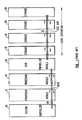
- This invention relates to computer systems in which peripheral units are interconnected with a CPU via an input/output bus and particularly relates to an expanded computer system having a plurality of modular units serially connected to a main bus and an expansion bus.
- Figure 1 shows a conventional, expanded computer system having a main bus 80 and an expansion bus 70.
- a system controller 10 Connected to the main bus 80 is a system controller 10 and a plurality of processors 12, 14, etc., which terminate in a controller module 20.
- the controller module 20 is itself connected to an expansion bus and is followed by a plurality of serially connected storage units 30, 40, 50 and 60.
- Figure 2 shows a simplified diagram of a typical modular unit 202 as it appears when physically connected to the expansion bus.
- Modular unit 202 would include drive unit 5 attached to a mother board 8.
- Mother board 8 would be connected to adjacent modular units by input header 7 which is coupled to drive 5 by a plurality of trace lines 6.
- input header 7 which is coupled to drive 5 by a plurality of trace lines 6.
- microprocessor 1 Within the drive 5, is a microprocessor 1 which is coupled to an ID header 2 by internal lines 4.
- the ID header 2 is in turn provided with a plurality of ID pins 3 which serve to provide the address for the modular unit shown in Figure 2.
- the ID headers are typically located deep within a recess in the drive housing and it has been very difficult for an end user to physically obtain access to the ID pin to provide the desired jumper connection. In order to make the proper jumper connections, it has been necessary to either insert fingers deep inside these recessed areas or to actually take the drive unit apart. Also, an unsophisticated end user might have absolutely no knowledge of the need to jumper the identification pins, and might experience difficulty in conveniently locating the pins even if aware of the need to provide some identification scheme at the point of end use.
- the invention comprises an automatic, self addressing technique for assigning addresses to modular units connected to a computer system bus.
- the invention comprises the method of initially generating a unique address in a controller module and thereafter transferring the unique address to the next expansion module.
- the expansion module receives the unique address, is identified by the unique address, and generates a new unique address using the received unique address. Thereafter the expansion module transfers the newly generated address to the next expansion module which likewise uses the received address to identify itself. The foregoing steps are repeated until each expansion module has been identified by a unique address.
- the unique address is provided by coupling grounding signals to the identification pins.
- a Read Only Memory (ROM) is used to receive the unique address and to generate a new address for transferring to the next module.
- a cable is used to connect the received unique addressed to the ID pins.
- Figure 1 is a block diagram of a modular computer system having a main bus 80 called an X bus and an expansion bus 70, in this case, an SCSI bus.
- the main system controller 10 is connected to the main bus 80, followed by a plurality of serially connected processor modules 12, 14 and 20.
- Processor module 20 in the example shown in Figure 1, comprises an SCSI controller module and serves to terminate the main bus.
- An expansion bus 70 is connected to the SCSI controller module 20.
- a plurality of serially connected expansion modules consisting of storage modules 30, 40, 50, and 60 are coupled to the expansion bus following the SCSI controller 20.
- processor modules coupled to the main bus would be, for example, voice, communication or other such processors
- storage modules connected to the expansion bus would typically comprise disk, optical or tape type storage devices.
- the maximum distance that a module can be located on the main bus from the system controller is 24 inches.
- the processor modules and the system controller are interconnected to each other using a 120 pin connector device.
- problems inherent in the system include there being a maximum distance permissible for extension from the system controller and there being a need for some scheme to identify the modules connected to the system controller to eliminate command ambiguities.
- an SCSI controller module would terminate the main bus and would have coupled to it an expansion bus having a plurality of storage modules coupled thereto.
- the SCSI controller module serves to extend the operation of the main bus in that the signals are not propagated from the main bus to the storage devices on the expansion bus but signals are transferred from the SCSI controller down the expansion bus to the storage units.
- Figure 2 depicts a typical module. Shown in Figure 2 are lines 70 from an SCSI controller which terminate in a 44 pin connector 7A at the output side of a previous mother board 8A.
- Connector 7A is coupled to the input side of motherboard 8 via 44 pin connector 7.
- Mother board 8 has located thereon a main drive unit 5.
- the 44 pin connector 7A is coupled to the input of drive unit 5 by a plurality of trace lines 6.
- the output of drive unit 5 is coupled to an output 44 pin connector 7B by output trace lines 6B.
- Drive unit 5 includes mini microprocessor 1, an ID header 2, and ID pins 3 within ID header 2.
- ID header 2 is coupled to the microprocessor by an internal communications line 4.
- the connectors, traces lines, and other input/output means form part of the SCSI bus.
- ID pins 3 include one column of pins 24 adjacent another column of pins 23.
- one column 24 of ID pins is configured such that each pin is coupled through a resistor to a positive voltage. Further, lines 4 tap from the resistors to the microprocessor. Thus, in normal operation, the lines 4 from ID pins in column 24 would provide a positive voltage to microprocessor 4. On the other hand, ID pins in column 23 are coupled to ground. Thus, in order to simulate a zero for the ID pins shown in Figure 3, jumpers have been used to connect selected pins in column 23 to selected pins in column 24, to thereby short selected pins to ground. By selectively jumpering pairs of pins, the prior art technique has permitted identification of modules by simulating 1's and 0's in the microprocessor.
- Microprocessor 1 has therefore been able to determine the address for the modular unit by translating the digital representation of the bits provided over communications line 4.
- a digital 011 signal is provided to microprocessor 1 which serves to identify the modular unit as unit number 6.
- one problem of the above configuration is that it limits the fungibility of modular units.
- This problem could be solved somewhat by placing jumpers on the modular units when the units are manufactured.
- a resulting problem is that the units would be committed to the serial location as placed thereon by the manufacturer and would again not have the flexibility to be located at any point along the expansion bus.
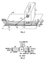
- Figure 4 shows a modular unit in accordance with the invention.
- modular expansion unit 200 which comprises a mother board 8, a drive unit 5, an ID header (connector) 130 and trace lines 6.
- Connector 130 is a 44 pin connector and couples the input side of mother board 8 to the output side of the previous motherboard in an adjacent modular unit on the expansion bus.
- Trace lines 6 couple the input header 130 to the drive unit 5.
- Output trace lines 9 couple the drive unit 5 to an output header 130.
- Lines 70 represent input lines from an adjacent previous module such as a SCSI controller.
- Line 90 represents output lines to the next SCSI module such as a next storage unit.
- Figure 4 also shows a plurality of trace lines 120 that are coupled from the input header 130 to ROM 100.
- Cable 110 is coupled from connector pins (not shown) on ROM 100 to ID pins 3 in drive header 2.
- Drive header 2 is coupled to microprocessor 1 by an internal communication line 4.
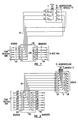
- FIG. 5 is a simplified block diagram of the ROM circuit 100 included in the modular expansion unit in accordance with the invention.
- ROM circuit 100 receives an address signal, ADDRESS(N), which is coupled to the input of ROM 100 from input header 130 by trace lines 120.
- the ADDRESS(N) signal is coupled through cable 110 to the ID header and the ID pins.
- ROM unit 100 takes the address signal provided thereto via trace lines 120 and generates a new data output which is the address for the next expansion module unit.
- the address generated is merely ADDRESS(N) plus 1.
- FIG. 6 shows a flow diagram of the steps in accordance with the invention.
- the method starts when a ROM in the SCSI controller generates an ADDRESS(1) equal to 1.
- the ROM controller would next transfer the address to the ROM unit in the next adjacent, serially connected expansion module via the connectors and trace lines.
- the ROM on the receiving module, ROM (N) would receive ADDRESS(N) from the ROM in the previous expansion module.
- ROM(N) would thereby transfer the ADDRESS(N) to the drive (N) via the cable coupled from pins on the ROM to the ID pins in the ID header, and thereafter through the internal communication line to the microprocessor in the drives (N).
- ROM(N) would use ADDRESS (N) to generate a data output, ADDRESS (N+1), which is provided as the address for the next adjacent, serially connected, expansion module unit.
- ADDRESS N+1
- the address for the next unit is simply the address provided for the instant ROM(N), plus 1. For example, if the address provided to the ROM unit were 2, then the address provided out would be 3.
- ADDRESS(N+1) is thereafter coupled from the output side of ROM(N) by a plurality of trace lines, which form a part of the expansion bus, to the output header.
- the output header for the Nth module couples the new address, ADDRESS(N+1), to the input header of the next adjacent mother board.
- Figure 7 is a detailed block diagram of one embodiment of the invention.
- the purpose of the configuration shown in Figure 7 is to provide to the microprocessor in the drive unit an address identifying the module as unit 5.
- the Id header has therein, 6 ID pins 3: voltage connected pins 1, 2, 3 and grounded pins 4, 5 and 6.
- the configuration according to the invention no longer requires that jumpers between adjacent pins provide the digital ID to the microprocessor, so that it is no longer required that pins, 4, 5 and 6 be utilized.
- grounding signals are provided to selected pins using the input signals provided to the ROM on lines 1, 2 and 3.
- Input lines 4, 5 and 6, therefore, are in the nature of spare lines and are not necessarily needed in the configuration shown in Figure 7.
- the problem of providing an address of "5" according to the embodiment in Figure 7 is a problem of simulating to the microprocessor a 1, a 0 and a 1 without having to provide jumpers to physically ground pins 1, 2 and 3.
- this problem is solved by providing grounding signals along selected input lines to the ROM.
- Input line 1 is provided with a 1 signal which in this instance is a low signal which serves to leave line 1 at the high voltage level.
- Input line 2 to the ROM is provided with a 0 signal which is a high (grounding) signal which serves to drive pin 2 in ID header 2 to ground.
- Line 3 is provided with a 1 signal, or a low signal, which serves to leave pin 3 in ID header 2 at a high level.
- a 1 signal or a low signal, which serves to leave pin 3 in ID header 2 at a high level.
- ROM 100 also takes the "101" address and processes these signals to generate an output signal that is to be used as the address for the next ROM. Since in this instance the input signal was 5, the output signal provided is 6 so that the next adjacent unit would be addressed at one higher than the instant ROM unit.
- ROM 100 Since the digital representation for 6 is 011, in this configuration, ROM 100 provides as output for line 1, a 0 ;for line 2, a 1; and for line 3, a 1. Thus, the signal provided on line 1 will be a grounding signal to drive pin 1 in the ID header in the next module to ground.
- Figure 8 depicts another ID configuration in accordance with another embodiment of the invention.
- the ID header is provided with 16 ID pins, consisting of two columns, 27 and 28, of 8 pins each.
- the grounded pins in column 28 are used as spares and need not be used in accordance with the invention.
- the ID pins in Figure 8 are not used to provide to the microprocessor a digital representation of the module address. Rather, the address is determined based solely on which particular pin in column 27 is coupled to ground by jumpering to a corresponding pin in column 28. For example, if pin 1 of column 27 in the ID header is jumpered to a ground pin in column 28, the address for the unit in Figure 8 would thereby be designated as "1". Similarly, if the 4 pin were connected to ground, that would indicate that the address for the unit using the ID header in Figure 8 would be a 4.
- the problem solved according to the invention for the embodiment shown in Figure 8 is the problem of simulating a ground at the particular pin that is to identify the address for the particular drive unit.
- ROM 100 has connected to its input side a plurality of input lines 120, numbered 0 through 7 and has connected to its output side a plurality of output lines 140, numbered 0 through 7.
- Lines 120 couple an address signal received from the previous ROM to ROM 100.
- Output lines 140 couple a new address signal generated by ROM 100 to the output header.
- the address for the modular unit in Figure 8 is to be "2".
- an "on” signal would be provided on line 2 which would be coupled to pin 2 of column 27 on the ROM.
- This "on” signal would be coupled from pin 2 on the ROM to the number 2 pin of column 27 in the ID header.
- the effect of the "on” signal is to drive the voltage at pin 2 of column 27 in the ID header to ground, thus simulating the jumpering arrangement. Because the voltage at ID pin 2 is driven to ground, the microprocessor recognizes that the address for the module is 2.
- the ROM would take the received address which comprises an "on”, (grounding) signal on line 2, would process that information, and would generate an addressing signal for the next adjacent ROM. Thus, in this instance, since line 2 is received in the "on” condition the ROM would generate an on signal on line 3, thereby causing the next serial module to be addressed as address 3.
- the ROM used in accordance with the invention is a mailbox type ROM wherein an address is supplied as an input into the ROM and data is automatically supplied as an output from the ROM.
- an address is provided on the input side of the ROM which is translated to a mailbox inside the ROM.
- the ROM automatically takes data inside the mailbox and provides that data as the output address for the next adjacent ROM.
- the mailboxes are preassigned through a conventional fuse link process. According to the invention shown in the embodiments of Figure 7 and 8, the input addressing signal must be provided continuously through the ROM's.
- the voltage used to drive the pins to ground is typically in the range of 5 volts.
- the low and off voltage signals would typically be 0 volts.
- a modular unit may be placed at any location along the bus so long as all the units along the bus are provided with the same automatic addressing scheme.
- each unit will automatically be addressed according to an input signal and will generate an address to be provided to a next module that is one more than the address received by that particular module.
- the cable hook-up from the ROM to the ID headers is provided as a standard part of the configuration package.
- the invention provides a scheme that permits automatic, unique addressing of expansion modules without relying on the main system controller.
- the invention facilitates expanding the length of modular computer systems by providing a means for uniquely identifying modular units beyond the maximum operating length of the main system controller.
Landscapes
- Engineering & Computer Science (AREA)
- Theoretical Computer Science (AREA)
- Physics & Mathematics (AREA)
- General Engineering & Computer Science (AREA)
- General Physics & Mathematics (AREA)
- Bus Control (AREA)
- Microcomputers (AREA)
- Small-Scale Networks (AREA)
Applications Claiming Priority (2)
| Application Number | Priority Date | Filing Date | Title |
|---|---|---|---|
| US07/177,704 US5148389A (en) | 1988-04-05 | 1988-04-05 | Modular expansion bus configuration |
| US177704 | 1988-04-05 |
Publications (2)
| Publication Number | Publication Date |
|---|---|
| EP0336708A2 true EP0336708A2 (de) | 1989-10-11 |
| EP0336708A3 EP0336708A3 (de) | 1991-02-06 |
Family
ID=22649654
Family Applications (1)
| Application Number | Title | Priority Date | Filing Date |
|---|---|---|---|
| EP19890303312 Withdrawn EP0336708A3 (de) | 1988-04-05 | 1989-04-04 | Modulare Erweiterungsbuskonfiguration |
Country Status (5)
| Country | Link |
|---|---|
| US (1) | US5148389A (de) |
| EP (1) | EP0336708A3 (de) |
| JP (1) | JPH02204851A (de) |
| AU (1) | AU3241789A (de) |
| CA (1) | CA1319443C (de) |
Cited By (8)
| Publication number | Priority date | Publication date | Assignee | Title |
|---|---|---|---|---|
| EP0467305A2 (de) * | 1990-07-19 | 1992-01-22 | Sony Corporation | Gerät zur Verbindung elektronischer Geräte |
| FR2723793A1 (fr) * | 1994-08-19 | 1996-02-23 | Siemens Ag | Procede d'association d'adresses |
| US5539390A (en) * | 1990-07-19 | 1996-07-23 | Sony Corporation | Method for setting addresses for series-connectd apparatuses |
| EP0843260A1 (de) * | 1996-11-15 | 1998-05-20 | Digital Equipment Corporation | Automatische Adressenzuweisung für Plattenlaufwerken enthaltende Gestelle sowie Fehlererkennungsverfahren und Gerät |
| WO2000014645A1 (en) * | 1998-09-04 | 2000-03-16 | Qlogic Corporation | Method and apparatus for comparing an address sent on a bus to a device's assigned address or addresses |
| EP1008939A2 (de) * | 1998-12-11 | 2000-06-14 | Hartmut B. Dr. Brinkhus | Selbstkonfigurierendes modulares Elektroniksystem, insbesondere Computersystem |
| JP2001093267A (ja) * | 1999-08-12 | 2001-04-06 | Hewlett Packard Co <Hp> | オートチェンジャ・モジュールを積み重ね可能にする装置 |
| DE10120586A1 (de) * | 2001-04-26 | 2002-11-07 | Tenovis Gmbh & Co Kg | Modulare Trägervorrichtung zum Tragen von Baugruppen mit eindeutiger Adressvergabe |
Families Citing this family (30)
| Publication number | Priority date | Publication date | Assignee | Title |
|---|---|---|---|---|
| CA1338639C (en) * | 1989-09-26 | 1996-10-08 | Seiichi Kubo | Communication control device |
| US5081092A (en) * | 1990-01-08 | 1992-01-14 | Ford Motor Company | Oxidation catalyst with modified platinum structure |
| US5086026A (en) * | 1990-01-08 | 1992-02-04 | Ford Motor Company | Reduction catalyst with modified rhodium structure |
| JPH04157550A (ja) * | 1990-10-22 | 1992-05-29 | Toshiba Corp | パーソナルコンピュータシステム |
| FR2671884A1 (fr) * | 1991-01-17 | 1992-07-24 | Moulinex Sa | Procede d'attribution d'adresses dans un reseau domotique. |
| JPH0823856B2 (ja) * | 1991-02-22 | 1996-03-06 | インターナショナル・ビジネス・マシーンズ・コーポレイション | コンピュータシステムおよびその動作方法 |
| US5317693A (en) * | 1991-04-04 | 1994-05-31 | Digital Equipment Corporation | Computer peripheral device network with peripheral address resetting capabilities |
| JPH0715665B2 (ja) * | 1991-06-10 | 1995-02-22 | インターナショナル・ビジネス・マシーンズ・コーポレイション | パーソナルコンピユータ |
| US5333277A (en) * | 1992-01-10 | 1994-07-26 | Exportech Trading Company | Data buss interface and expansion system |
| US5353413A (en) * | 1992-03-19 | 1994-10-04 | Aeg Transportation Systems, Inc. | Method and apparatus for christening a trainline monitor system |
| JPH06139182A (ja) * | 1992-10-27 | 1994-05-20 | Sony Corp | 情報処理装置、拡張基板、および拡張筐体システム |
| US5680556A (en) * | 1993-11-12 | 1997-10-21 | International Business Machines Corporation | Computer system and method of operation thereof wherein a BIOS ROM can be selectively locatable on diffeent buses |
| US5636342A (en) * | 1995-02-17 | 1997-06-03 | Dell Usa, L.P. | Systems and method for assigning unique addresses to agents on a system management bus |
| JP3359496B2 (ja) * | 1996-06-14 | 2002-12-24 | 沖電気工業株式会社 | 伝送装置識別番号付与方法、伝送装置及び伝送システム管理装置 |
| US5918241A (en) * | 1997-02-21 | 1999-06-29 | Lsi Logic Corporation | Method and apparatus for setting a plurality of addresses |
| KR100551191B1 (ko) * | 1997-05-16 | 2006-05-25 | 매그나칩 반도체 유한회사 | 컴퓨터 시스템에서의 논리 유니트 유일 식별 방법 |
| JP3304292B2 (ja) * | 1997-09-12 | 2002-07-22 | インターナショナル・ビジネス・マシーンズ・コーポレーション | 外部機器の装着や識別を検出するための自動検出装置、情報処理機器、及び外部機器 |
| US6553437B1 (en) * | 1998-06-15 | 2003-04-22 | Texas Instruments Incorporated | Addressing and communication for multiple-chip optical sensor arrays |
| US8713641B1 (en) | 1998-12-08 | 2014-04-29 | Nomadix, Inc. | Systems and methods for authorizing, authenticating and accounting users having transparent computer access to a network using a gateway device |
| US7194554B1 (en) | 1998-12-08 | 2007-03-20 | Nomadix, Inc. | Systems and methods for providing dynamic network authorization authentication and accounting |
| US8266266B2 (en) | 1998-12-08 | 2012-09-11 | Nomadix, Inc. | Systems and methods for providing dynamic network authorization, authentication and accounting |
| US7475031B1 (en) * | 1999-09-07 | 2009-01-06 | Novell, Inc. | Communication interface for providing accounting support for print services |
| US6898720B2 (en) * | 2002-12-24 | 2005-05-24 | Sunrise Telecom Incorporated | Scalable extensible network test architecture |
| US8239594B2 (en) * | 2005-11-10 | 2012-08-07 | Datacard Corporation | Modular card issuance system and method of operation |
| US9904330B2 (en) * | 2014-10-10 | 2018-02-27 | Sanmina Corporation | Base board architecture for a server computer and method therefor |
| CN106843007B (zh) * | 2017-03-07 | 2023-03-31 | 江苏安科瑞电器制造有限公司 | 一种模块化电力仪表及其编址方法 |
| US10551897B2 (en) | 2017-06-07 | 2020-02-04 | Intel Corporation | Combining presence detect pin with device management bus reset and power disable |
| US10409737B2 (en) * | 2017-06-07 | 2019-09-10 | Intel Corporation | Apparatus, system, and method for positionally aware device management bus address assignment |
| US10216685B1 (en) * | 2017-07-19 | 2019-02-26 | Agiga Tech Inc. | Memory modules with nonvolatile storage and rapid, sustained transfer rates |
| CN107643997A (zh) * | 2017-08-30 | 2018-01-30 | 浙江工业大学 | 一种扩展模块自动寻址的方法 |
Citations (3)
| Publication number | Priority date | Publication date | Assignee | Title |
|---|---|---|---|---|
| FR2245028A1 (de) * | 1973-09-24 | 1975-04-18 | Siemens Ag | |
| JPS5775353A (en) * | 1980-10-29 | 1982-05-11 | Aisuke Katayama | High-speed addition system of rom connection type |
| EP0153015A2 (de) * | 1984-02-07 | 1985-08-28 | Stc Plc | Integrierte Wafer-Scale-Schaltungen |
Family Cites Families (6)
| Publication number | Priority date | Publication date | Assignee | Title |
|---|---|---|---|---|
| US4468729A (en) * | 1981-06-29 | 1984-08-28 | Sperry Corporation | Automatic memory module address assignment system for available memory modules |
| DE3347357A1 (de) * | 1983-12-28 | 1985-07-11 | Siemens AG, 1000 Berlin und 8000 München | Einrichtung zum vergeben von adressen an steckbare baugruppen |
| US4727475A (en) * | 1984-05-18 | 1988-02-23 | Frederick Kiremidjian | Self-configuring modular computer system with automatic address initialization |
| US4760553A (en) * | 1985-06-03 | 1988-07-26 | International Business Machines Corporation | Terminal system configuration tracing method and apparatus |
| GB2180972A (en) * | 1985-09-27 | 1987-04-08 | Philips Electronic Associated | Generating addresses for circuit units |
| US4951248A (en) * | 1988-03-04 | 1990-08-21 | Sun Microsystems, Inc. | Self configuring memory system |
-
1988
- 1988-04-05 US US07/177,704 patent/US5148389A/en not_active Expired - Lifetime
-
1989
- 1989-04-04 CA CA000595581A patent/CA1319443C/en not_active Expired - Fee Related
- 1989-04-04 JP JP1085645A patent/JPH02204851A/ja active Pending
- 1989-04-04 EP EP19890303312 patent/EP0336708A3/de not_active Withdrawn
- 1989-04-04 AU AU32417/89A patent/AU3241789A/en not_active Abandoned
Patent Citations (3)
| Publication number | Priority date | Publication date | Assignee | Title |
|---|---|---|---|---|
| FR2245028A1 (de) * | 1973-09-24 | 1975-04-18 | Siemens Ag | |
| JPS5775353A (en) * | 1980-10-29 | 1982-05-11 | Aisuke Katayama | High-speed addition system of rom connection type |
| EP0153015A2 (de) * | 1984-02-07 | 1985-08-28 | Stc Plc | Integrierte Wafer-Scale-Schaltungen |
Non-Patent Citations (1)
| Title |
|---|
| PATENT ABSTRACTS OF JAPAN, vol. 6, no. 159 (P-136)[1037], 20th August 1982; & JP-A-57 075 353 (AISUKE KATAYAMA) 11-05-1982 * |
Cited By (17)
| Publication number | Priority date | Publication date | Assignee | Title |
|---|---|---|---|---|
| EP0467305A2 (de) * | 1990-07-19 | 1992-01-22 | Sony Corporation | Gerät zur Verbindung elektronischer Geräte |
| EP0722224A2 (de) * | 1990-07-19 | 1996-07-17 | Sony Corporation | Verfahren zur Aufstellung von Adressen für elektronische Geräte |
| US5539390A (en) * | 1990-07-19 | 1996-07-23 | Sony Corporation | Method for setting addresses for series-connectd apparatuses |
| EP0722224A3 (de) * | 1990-07-19 | 1996-08-07 | Sony Corp | |
| EP0467305B1 (de) * | 1990-07-19 | 1997-07-02 | Sony Corporation | Gerät zur Verbindung elektronischer Geräte |
| US5712834A (en) * | 1990-07-19 | 1998-01-27 | Sony Corporation | Control apparatus for data reproduction and recording devices |
| FR2723793A1 (fr) * | 1994-08-19 | 1996-02-23 | Siemens Ag | Procede d'association d'adresses |
| US5740379A (en) * | 1994-08-19 | 1998-04-14 | Siemens Aktiengesellschaft | Method for generating unique addresses for electrical devices from input bit patterns being verifiable for admissibility |
| EP0843260A1 (de) * | 1996-11-15 | 1998-05-20 | Digital Equipment Corporation | Automatische Adressenzuweisung für Plattenlaufwerken enthaltende Gestelle sowie Fehlererkennungsverfahren und Gerät |
| WO2000014645A1 (en) * | 1998-09-04 | 2000-03-16 | Qlogic Corporation | Method and apparatus for comparing an address sent on a bus to a device's assigned address or addresses |
| EP1008939A2 (de) * | 1998-12-11 | 2000-06-14 | Hartmut B. Dr. Brinkhus | Selbstkonfigurierendes modulares Elektroniksystem, insbesondere Computersystem |
| EP1008939A3 (de) * | 1998-12-11 | 2002-01-02 | Hartmut B. Dr. Brinkhus | Selbstkonfigurierendes modulares Elektroniksystem, insbesondere Computersystem |
| US6516377B1 (en) | 1998-12-11 | 2003-02-04 | Hartmut B. Brinkhus | Self-configuring modular electronic system |
| JP2001093267A (ja) * | 1999-08-12 | 2001-04-06 | Hewlett Packard Co <Hp> | オートチェンジャ・モジュールを積み重ね可能にする装置 |
| EP1076283A3 (de) * | 1999-08-12 | 2003-07-23 | Hewlett-Packard Company, A Delaware Corporation | System zur Stapelung von automatischen Wechslermodulen |
| DE10120586A1 (de) * | 2001-04-26 | 2002-11-07 | Tenovis Gmbh & Co Kg | Modulare Trägervorrichtung zum Tragen von Baugruppen mit eindeutiger Adressvergabe |
| DE10120586B4 (de) * | 2001-04-26 | 2010-09-30 | Tenovis Gmbh & Co. Kg | Modulare Trägervorrichtung zum Tragen von Baugruppen mit eindeutiger Adressvergabe |
Also Published As
| Publication number | Publication date |
|---|---|
| EP0336708A3 (de) | 1991-02-06 |
| CA1319443C (en) | 1993-06-22 |
| AU3241789A (en) | 1989-10-12 |
| JPH02204851A (ja) | 1990-08-14 |
| US5148389A (en) | 1992-09-15 |
Similar Documents
| Publication | Publication Date | Title |
|---|---|---|
| EP0336708A2 (de) | Modulare Erweiterungsbuskonfiguration | |
| US5357621A (en) | Serial architecture for memory module control | |
| EP0221303B1 (de) | Automatische E/A-Adressenzuweisung | |
| US6002638A (en) | Memory device having a switchable clock output and method therefor | |
| US4885482A (en) | Multiple computer interface circuit board | |
| EP0121381B1 (de) | Gerät zur Speicheridentifizierung | |
| JP3168552B2 (ja) | メモリ・アクセス制御システム及びその方法 | |
| US5727184A (en) | Method and apparatus for interfacing between peripherals of multiple formats and a single system bus | |
| US6438625B1 (en) | System and method for automatically identifying slots in a backplane | |
| US5204669A (en) | Automatic station identification where function modules automatically initialize | |
| US6347367B1 (en) | Data bus structure for use with multiple memory storage and driver receiver technologies and a method of operating such structures | |
| EP0044949A1 (de) | Dynamisches Terminal-Adressen-Zuweisungsverfahren und Vorrichtung | |
| US7383416B2 (en) | Method for setting a second rank address from a first rank address in a memory module | |
| JPS58127259A (ja) | デ−タ処理システムにおけるメモリモジユ−ル選択及び再構成装置 | |
| EP0224877A2 (de) | Schnittstelle für universalen Modul | |
| JPH086685A (ja) | 相互接続装置及びそれを使用するケーブル管理装置 | |
| US5465106A (en) | Generic driver interface card | |
| US5598540A (en) | Memory module including read-write memory and read-only configuration memory accessed only sequentially and computer system using at least one such module | |
| CA2122079C (en) | Universal cd-rom interface | |
| US4607347A (en) | Microcomputer system employing program cartridges | |
| EP0200198B1 (de) | Einrichtung zur Erweiterung der Speicherkapazität | |
| US5987533A (en) | Automatically configuring SCSI device addresses using SCSI controller storing predetermined ID and, producing address signals for transferring to peripheral device via SCSI ID input means | |
| US5564059A (en) | Simplified protocol for expanding a fixed width bus in an industrial controller | |
| US4937785A (en) | Visual signal processing backplane bus | |
| US20020052994A1 (en) | Section access for pc hard drive and the like |
Legal Events
| Date | Code | Title | Description |
|---|---|---|---|
| PUAI | Public reference made under article 153(3) epc to a published international application that has entered the european phase |
Free format text: ORIGINAL CODE: 0009012 |
|
| AK | Designated contracting states |
Kind code of ref document: A2 Designated state(s): AT BE CH DE ES FR GB GR IT LI LU NL SE |
|
| PUAL | Search report despatched |
Free format text: ORIGINAL CODE: 0009013 |
|
| AK | Designated contracting states |
Kind code of ref document: A3 Designated state(s): AT BE CH DE ES FR GB GR IT LI LU NL SE |
|
| 17P | Request for examination filed |
Effective date: 19910411 |
|
| 17Q | First examination report despatched |
Effective date: 19930706 |
|
| STAA | Information on the status of an ep patent application or granted ep patent |
Free format text: STATUS: THE APPLICATION IS DEEMED TO BE WITHDRAWN |
|
| 18D | Application deemed to be withdrawn |
Effective date: 19971216 |