EP0336444A2 - Integrierte Halbleiterschaltkreisanordnung mit verbesserter Eingangs-/ Ausgangsschnittstellenschaltung - Google Patents
Integrierte Halbleiterschaltkreisanordnung mit verbesserter Eingangs-/ Ausgangsschnittstellenschaltung Download PDFInfo
- Publication number
- EP0336444A2 EP0336444A2 EP89106210A EP89106210A EP0336444A2 EP 0336444 A2 EP0336444 A2 EP 0336444A2 EP 89106210 A EP89106210 A EP 89106210A EP 89106210 A EP89106210 A EP 89106210A EP 0336444 A2 EP0336444 A2 EP 0336444A2
- Authority
- EP
- European Patent Office
- Prior art keywords
- input
- signal
- semiconductor integrated
- integrated circuit
- external terminal
- Prior art date
- Legal status (The legal status is an assumption and is not a legal conclusion. Google has not performed a legal analysis and makes no representation as to the accuracy of the status listed.)
- Granted
Links
Images


Classifications
-
- G—PHYSICS
- G01—MEASURING; TESTING
- G01R—MEASURING ELECTRIC VARIABLES; MEASURING MAGNETIC VARIABLES
- G01R31/00—Arrangements for testing electric properties; Arrangements for locating electric faults; Arrangements for electrical testing characterised by what is being tested not provided for elsewhere
- G01R31/26—Testing of individual semiconductor devices
-
- G—PHYSICS
- G01—MEASURING; TESTING
- G01R—MEASURING ELECTRIC VARIABLES; MEASURING MAGNETIC VARIABLES
- G01R31/00—Arrangements for testing electric properties; Arrangements for locating electric faults; Arrangements for electrical testing characterised by what is being tested not provided for elsewhere
- G01R31/28—Testing of electronic circuits, e.g. by signal tracer
- G01R31/317—Testing of digital circuits
- G01R31/3181—Functional testing
- G01R31/3185—Reconfiguring for testing, e.g. LSSD, partitioning
- G01R31/318522—Test of Sequential circuits
-
- G—PHYSICS
- G01—MEASURING; TESTING
- G01R—MEASURING ELECTRIC VARIABLES; MEASURING MAGNETIC VARIABLES
- G01R31/00—Arrangements for testing electric properties; Arrangements for locating electric faults; Arrangements for electrical testing characterised by what is being tested not provided for elsewhere
- G01R31/28—Testing of electronic circuits, e.g. by signal tracer
- G01R31/317—Testing of digital circuits
- G01R31/3181—Functional testing
- G01R31/3183—Generation of test inputs, e.g. test vectors, patterns or sequences
-
- H10P74/00—
Definitions
- the present invention generally relates to a semiconductor integrated circuit device having an improved input/output interface circuit, and in particular to an input/output interface circuit which is designed to be subjected to a variety of tests with ease.
- LSI devices large scale integrated circuit devices
- LSI devices are subjected to a variety of tests in order to investigate whether or not LSI devices operate correctly.
- LSI devices are activated under a specified operational condition, and it is investigated whether or not LSI devices operate without exhibiting abnormality.
- Functional test and DC characteristic test are typical of test of LSI devices.
- a predetermined pattern is supplied to an LSI device, and it is investigated whether or not a corresponding pattern is output from the LSI device.
- DC test direct current characteristic test
- an external terminal other than an external terminal to be tested is set to a specified condition. In this state, a specified current is made applied or outputted to the external terminal to be tested. Then, the DC voltage of the external terminal to be tested is measured. Thereby, it is determined, based on the measured voltage, as to whether or not the LSI device can operate correctly in view of DC characteristics.
- LSI devices includes external terminals, input/output circuits, and internal logic circuits.
- a signal applied to an external terminal other than an external terminal to be tested passes through an input/output interface circuit, an internal logic, and input/output interface circuit. Then a signal responsive to the applied signal appears at the external terminal to be tested. That is, the applied signal such as a test pattern always passes through the internal logic circuit. For this reason, it is difficult to directly investigate the input/output interface circuit itself. In particular, it is very difficult to investigate that an input circuit which is a part of input/output interface circuits, operates correctly. Additionally, an external device which generates test patterns must be used in test. Moreover, it takes long to execute test programs to test LSI devices.
- a more specific object of the present invention to provide a semiconductor integrated circuit device having an improved input/output interface circuit which is directly and easily subjected to tests for investigating whether or not the input/output interface circuit operates correctly.
- Another object of the present invention is to provide a semiconductor integrated circuit device having an improved input/output interface circuit which is subjected to tests without using a specific test pattern generator.
- a semiconductor integrated circuit device including an external terminal; internal logic means for subjecting a first signal to a predetermined logic operation and outputting a second signal; and input/output interface means, connected to the internal logic means, for receiving an input signal through the external terminal and supplying the internal logic means with the input signal as the first signal and for outputting the second signal supplied from the internal logic means to the external terminal.
- the input/output interface means comprises input means, connected to the external terminal, for receiving the input signal and supplying the internal logic means with the same as the first signal; selection means, connected to the input means and the internal logic means, for selecting either the first signal supplied from the input means or the second signal supplied from the internal logic means; and output means, connected to the external terminal, for outputting the selected one of the first and second signals to the external terminal.
- a loop circuit is formed by the input means, selection means and output means, the loop circuit logically including an odd number of inverters.
- a semiconductor integrated circuit device comprising external terminal; internal logic means for subjecting a first signal to a predetermined logic operation and outputting a second signal; and input/output interface means, connected to the internal logic means, for receiving an input signal through the external terminal and supplying the internal logic means with the input signal as the first signal and for outputting the second signal supplied from the internal logic means to the external terminal.
- the input/output interface means comprises input means, connected to the external terminal, for receiving the input signal and supplying the internal logic means with the same as the first signal; and means, connected to input means and the external terminal, for outputting the first signal supplied from the input means to the external terminal at a predetermined time.
- a loop circuit is formed by the input means and the output means, the loop circuit logically including an odd number of inverters.
- an input circuit connected to an external input/output terminal 1 of an LSI includes an input buffer 2, and a D-type flip-flop 3, which is connected to an internal logic circuit (not shown) through an input data bus.
- An output circuit includes a D-type flip-flop 4 connected to the internal logic circuit through an output data bus, and a tri-state buffer 5 connected to the external input/output terminal 1.
- the flip-flop 3 latches a signal applied thereto when a second clock signal ⁇ 2 shown in FIG.2 rises.
- the flip-flop 4 latches a signal applied thereto when a first clock signal ⁇ 1 shown in FIG.2 rises.
- the tri-state buffer 5 is activated when a control signal TRS shown in FIG.2 is held at a low level (hereafter simply referred to L level). At this time, a signal on the output data bus appears at the external input/output terminal 1, as shown in FIG.2. With the tri-state buffer 5 closed, the external input/output terminal 1 is kept in a high impedance state (HiZ) as shown in FIG.2.
- an external terminal 9 is connected to an input circuit 7, which is connected to an internal logic circuit (not shown) through an input data bus IDB.
- the input circuit 7 is also connected to a selection circuit 10, which is connected to the internal logic circuit through an output data bus ODB.
- the selection circuit 10 selects either the input circuit 7 or the output data bus ODB.
- the selection circuit 10 is also connected to an output circuit 8, which is connected to the external terminal 9.
- the present invention has the following first to third essential features.
- the first essential feature of the present invention is that there is formed a loop circuit including the input circuit 7 and the output circuit 8.
- the second essential feature of the present invention is that the loop circuit logically has an odd number of inverter elements. In other words, when a signal is applied to the external terminal 9, and passes through the input circuit 7, the selection circuit 10 and the output circuit 8, an inverted signal of the applied signal is obtained at the external terminal 9.
- the third essential feature of the present invention is that the input circuit 7 and the output circuit 8 are separated from each other in view of operation. For example, the input circuit 7 is driven by a clock signal, which is different from a clock signal used for driving the output circuit 8.
- an input voltage signal of H level for example is applied to the external terminal 9.
- the applied signal passes through the input terminal 7 and is then selected by the selection circuit 10.
- the applied signal passes through the output circuit 8 and is then output to the external terminal 9.
- a signal of L level is output from the output circuit 8. That is, the external terminal 9 is switched to L level.
- the application of the input voltage signal is stopped.
- the L level of the external terminal 9 is applied to the input circuit 7.
- the output of the output circuit 8 is switched to H level.
- the input voltage signal is applied to the external terminal 9
- the voltage of the external terminal is alternately changed to L and H levels, when the input and output circuits 7 and 8 operate correctly.
- no alternate level change is observed at the external terminal 9
- FIG.4 is a schematic view of an example of the entire structure of the present invention.
- an internal logic circuit 110 there are formed an internal logic circuit 110, an input/output interfaces (hereafter simply referred to I/O interfaces) 120 and 130, and a plurality of external terminals 140.
- the I/O interfaces 120 and 130 are connected to the internal logic circuit 110 through data buses 150 including input data buses IDB and output data buses ODB as shown in FIG.3.
- the structure of FIG.3 is provided in the I/O interfaces 120 and 130.
- an external input/output terminal 17 corresponds to the external terminal 9 of FIG.3 and one of the external terminals 140 shown in FIG.4.
- the external input/output terminal 17 is simply referred to as external terminal.
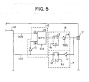
- An input buffer 11 and a D-type flip-flop 12 construct the input circuit 7 shown in FIG.3.
- a D-type flip-flop 15 and a tri-state buffer 16 construct the output circuit 8 shown in FIG.3.
- An inverter 13, and a multiplexer 14 served as a selector construct the selection circuit 10 shown in FIG.3.
- the flip-flop 12 latches the output signal of the input buffer 11 when the second clock signal ⁇ 2 shown in FIG.6 rises.
- the Q-terminal output of the flip-flop 12 is supplied to the internal circuit 110 through the input data bus IDB, and also to a B-terminal of the multiplexer 14 through the inverter 13.
- the inverter 13 is provided so that an odd number of inverters is included in a loop circuit consisting of the input circuit 7, the selection circuit 10 and the output circuit 8. In the alternative, the inverter 13 may be located in the input circuit 7 or the output circuit 8.
- the multiplexer 14 has an A-terminal to which a signal shown in FIG.6 is supplied from the internal logic circuit 110 through the output data bus ODB.
- the multiplexer 14 is controlled by a selection signal Sel, which is supplied from the internal circuit 110 or an external circuit supplied through another external terminal.
- the selected signal is supplied to the D-terminal of the flip-flop 15, which operates in synchronism with the first clock signal ⁇ 1.
- the Q-terminal of the flip-flop 15 is connected to the tri-state buffer 16, which is controlled by the control signal TRS shown in FIG.6.
- the control signal TRS is held at L level, the tri-state buffer 16 is kept at the active state.
- the control signal TRS at H level (a high level)
- the tri-state buffer 16 is held in high-impedance state.
- the first and second clock signals ⁇ 1 and ⁇ 2 and the control signal TRS are signals used in conventional LSI devices.
- Test of the input circuit 7 includes an input/output functional test and DC test.
- the flip-flops 12 and 15 are initially set in the set state by set signals applied to set terminals (S) thereof supplied from the external terminal or the internal logic circuit 110, for example.
- S set terminals
- the input/output functional test is described at first. It is now assumed that in this state, an input signal of H level is applied to the external terminal 17, as shown in FIG.6.
- the input signal passes through the input buffer 11 and is latched in synchronism with the rise of the second clock signal ⁇ 2 occurring at time t1.
- the latched input signal is supplied to the internal logic circuit 110 through the input data bus IDB, and the B-terminal of the multiplexer 14 through the inverter 13.
- the latched signal from the flip-flop 12 is inverted by the inverter 13.
- the multiplexer 14 is supplied with the selection signal Sel so as to select the B-terminal. Therefore, the multiplexer 14 passes the signal supplied from the inverter 13, and outputs the same to the flip-flop 15. Then the flip-flop 15 latches the supplied signal in synchronism with the rise of the first clock signal ⁇ 1 occurring at time t2. Then, the latched signal is supplied to the external terminal 17 through the tri-state buffer 16.
- the control signal TRS is kept at L level, as shown in FIG.6. It is noted that the application of the input signal is stopped at a certain time between t1 and t2.
- the voltage of the external terminal 17 falls at time t2.
- the fall of the voltage is supplied to the flip-flop 12 through the input buffer 11, and is latched therein in synchronism with the rise of the second clock signal ⁇ 2 occurring at time t3.
- the latched signal is supplied to the flip-flop 15 through the inverter 13 and the multiplexer 14, and is latched therein in synchronism with the rise of the first clock signal ⁇ 1 occurring at time t4. Then, the latched signal is output to the external terminal 17 through the tri-state buffer 16.
- the level of the external terminal 17 is alternately changed to L and H levels, when the input buffer 7 and the output buffer 8 operate correctly.
- the input circuit 7 or the output circuit 8 is determined to be in an abnormal state.
- the DC test is described below.
- the DC test is intended to investigate upper and lower threshold levels V 1H and V 1L of the input buffer 11.
- the input buffer 11 (a CMOS inverter, for example) is switched to a first state (L level for CMOS inverter) when the voltage applied thereto is equal to or higher than the upper threshold voltage, while switched to a second state (H level for CMOS inverter) when the voltage is equal to or lower than the lower threshold voltage.
- the control signal TRS is switched to H level at times t7 and t9 when the second clock signal ⁇ 2 rises, and is switched to L level at times t8 and t10 when the first clock signal ⁇ 1 rises.
- the external terminal 17 is alternately supplied with first and second voltages in synchronism with H-level durations of the control signals TRS .
- the first voltage is slightly higher than the upper threshold voltage V 1H , and is set equal to 2.2 volts in the case where the input buffer 11 operates in TTL level, for example.
- the second voltage is slightly lower than the lower threshold voltage V 1L , and is set equal to 0.8 volts in the case where the input buffer 11 operates in TTL level.
- the voltage V IN of the external terminal 17 is set equal to 2.2 volts during the H-level duration of the control signal TRS starting from time t7, and is again set equal to 2.2 volts during the next H-level duration starting from time t9.
- the input buffer 11 outputs a first specified positive voltage (a positive power source voltage Vcc, for example) when the first voltage (2.2 volts) is applied to the external terminal 17.
- the voltage signal is inverted by the inverter 13, and therefore a second specified negative voltage (a negative power source voltage Vss, for example) appears in synchronism with the rise of the first clock signal ⁇ 1.
- Vcc positive power source voltage
- Vss negative power source voltage
- the input buffer 11 outputs the negative power source voltage Vss, which is inverted by the inverter 13, and is then applied to the flip-flop 15 through the multiplexer 14. Then the positive power source voltage Vcc appears in synchronism with the rise of the first clock signal ⁇ 1.
- the above-mentioned operation is done in the duration between times t9 and t11 in FIG.6.
- the input buffer 7 can operate correctly.
- the input circuit 7 is made up of only cascaded inverters 18 and 19. That is, an input signal is entered in the input circuit 7 without being synchronized with a clock signal such as the clock signal ⁇ 2 used in the aforementioned first embodiment.
- the selection circuit 10 of FIG.7 is the same as the selection circuit 10 of FIG.5.
- the output circuit 8 is constructed by providing a flip-flop 20 between the flip-flop 15 and the tri-state buffer 16 of the output circuit 8 shown in FIG.5.
- the flip-flop 20 operates in synchronism with the clock signal ⁇ 2.
- the input circuit 7 is separated from the output circuit 8 in view of operation due to the presence of the two flip-flops 15 and 20.
- the inverter 13 is provided so that an odd number of inverters is logically included in the loop circuit.
- the second embodiment can operate in the same way as the first embodiment.
- the input circuit 7 of the third embodiment is the same as the input circuit 7 of the second embodiment.
- the selection circuit 10 of the third embodiment is made up of the the multiplexer 14, and a D-type flip-flop 21, which is driven by the first clock signal ⁇ 1.
- the Q -terminal of the flip-flop 21 is connected to the D-terminal of the flip-flop 20 of the output circuit 8. Since the output signal of the flip-flop 21 is extracted from the Q -terminal thereof, the flip-flop 21 may be considered as an inverter. As a result, the loop substantially has three inverters.
- the operation of the third embodiment is almost identical to that of the first and second embodiments.
- the third embodiment is simpler than the second embodiment.
- a fourth embodiment is illustrated in FIG.9.
- the input circuit 7 of the fourth embodiment is the same as the input circuit 7 used in the second and third embodiments.
- the selection circuit 10 is formed only by the multiplexer 14.
- the output circuit 8 is constructed by the flip-flops 15, 20, and an N-channel field effect transistor (hereafter simply referred to as NFET) 22. That is, the tri-state buffer 16 of the output circuit 7 shown in FIG.7 is replaced with the NFET 22.
- the NFET 22 is an open-drain FET, and has a function of inverting the input signal applied to the external terminal 17. In the initial state, the Q-terminal of the flip-flop 20 is at L level, and thereby the NFET is OFF.
- the input signal of H-level is applied to the external terminal 17.
- the signal passes through the input circuit 7 and the selection circuit 10, and is then latched in synchronism with the rise of the first clock signal ⁇ 1.
- the Q-output signal is latched in synchronism with the rise of the second clock signal ⁇ 2. Since the potential of the Q-terminal of the flip-flop 20 is high at this time, the NFET is turned ON. As a result, the external terminal 17 is switched to L level.
- the L level is applied to the input circuit 7. In this way, the voltage of the external terminal 17 is alternately switched to L and H levels.
- An external terminal 23 is an external input terminal. That is, an output signal supplied from the internal logic gate 110 is not output through the external input terminal 23.
- the input circuit 7 is made up of the inverter 11, a D-type flip-flop 24 and flip-flop 12.
- an output circuit 48 is provided as illustrated in FIG.10.
- the output circuit 48 of FIG.10 is constructed by inverters 13, 25, an NAND gate 26, an NOR gate 27, a P-channel MOS transistor 28, and an N-channel MOS transistor 29.
- the output circuit 48 and the input circuit 7 of FIG.10 form a loop circuit, which is activated when the input circuit 7 is tested.
- the input terminal of the inverter 13 is connected to the D-terminal of the flip-flop 12, and the output terminal thereof is connected to the NAND gate 26 and the NOR gate 27.
- the control signal TRS shown in FIG.6 is supplied to the NAND gate 26, and the NOR gate 27 through the inverter 25.
- the output terminal of the NAND gate 26 is connected to the gate of the PMOS transistor 28, and the output terminal of the NOR gate 27 is connected to the gate of the NMOS transistor 29.
- the drains of the PMOS transistor 28 and NMOS transistor 29 are connected to the external input terminal 23.
- the source of the PMOS transistor 28 is connected to a positive power source (Vcc), and the source of the NMOS transistor 29 is connected to a negative power source (ground).
- the control signal TRS is set to H level in the input/output functional test.
- the input signal applied to the external input terminal 23 is inverted by the inverter 13, and is applied to the NAND gate 26 and the NOR gate 27.
- the gate of the PMOS transistor 28 is set to H level
- the gate of the NMOS transistor 29 is set to H level. Therefore the NMOS transistor 29 makes the external input terminal 23 low, since the NMOS transistor 29 is turned ON.
- the L-level is applied to the input circuit 7. Therefore, the external input terminal 23 is switched to H level. In this way, the external input terminal 23 is alternately changed between H and L levels.
- control signal TRS is set to L level, and therefore the output circuit 48 is electrically separated from the external input terminal 23.
Landscapes
- Engineering & Computer Science (AREA)
- Physics & Mathematics (AREA)
- General Physics & Mathematics (AREA)
- General Engineering & Computer Science (AREA)
- Microelectronics & Electronic Packaging (AREA)
- Logic Circuits (AREA)
- Semiconductor Integrated Circuits (AREA)
- Tests Of Electronic Circuits (AREA)
- Testing Of Individual Semiconductor Devices (AREA)
Applications Claiming Priority (2)
| Application Number | Priority Date | Filing Date | Title |
|---|---|---|---|
| JP86871/88 | 1988-04-08 | ||
| JP63086871A JPH01259274A (ja) | 1988-04-08 | 1988-04-08 | 集積回路の試験方式 |
Publications (3)
| Publication Number | Publication Date |
|---|---|
| EP0336444A2 true EP0336444A2 (de) | 1989-10-11 |
| EP0336444A3 EP0336444A3 (de) | 1991-01-30 |
| EP0336444B1 EP0336444B1 (de) | 1995-02-15 |
Family
ID=13898887
Family Applications (1)
| Application Number | Title | Priority Date | Filing Date |
|---|---|---|---|
| EP89106210A Expired - Lifetime EP0336444B1 (de) | 1988-04-08 | 1989-04-07 | Integrierte Halbleiterschaltkreisanordnung mit verbesserter Eingangs-/ Ausgangsschnittstellenschaltung |
Country Status (5)
| Country | Link |
|---|---|
| US (1) | US4970410A (de) |
| EP (1) | EP0336444B1 (de) |
| JP (1) | JPH01259274A (de) |
| KR (1) | KR930000894B1 (de) |
| DE (1) | DE68921086T2 (de) |
Cited By (3)
| Publication number | Priority date | Publication date | Assignee | Title |
|---|---|---|---|---|
| FR2660071A1 (fr) * | 1990-03-23 | 1991-09-27 | Alcatel Radiotelephone | Systeme de test d'un circuit imprime pourvu de circuits integres et application de ce systeme au test d'un tel circuit imprime. |
| EP0525990A1 (de) * | 1991-07-02 | 1993-02-03 | Hewlett-Packard Company | Testen von Eingangs- und Ausgangsstufen in integrierten Schaltungen |
| EP1132816A3 (de) * | 2000-03-02 | 2005-09-07 | Texas Instruments Incorporated | Automatische Erkennung der Verbindung zwischen einem Emulator und einem Zielgerät |
Families Citing this family (23)
| Publication number | Priority date | Publication date | Assignee | Title |
|---|---|---|---|---|
| JP2566005B2 (ja) * | 1989-03-03 | 1996-12-25 | 株式会社東芝 | 入力切換装置 |
| US5079442A (en) * | 1990-03-28 | 1992-01-07 | Advanced Micro Devices, Inc. | Apparatus adaptable for use as a replacement output driver in a signal generating circuit |
| US5498976A (en) * | 1990-10-26 | 1996-03-12 | Acer Incorporated | Parallel buffer/driver configuration between data sending terminal and data receiving terminal |
| JP2563679B2 (ja) * | 1991-01-24 | 1996-12-11 | シャープ株式会社 | 双方向入出力信号分離回路 |
| US5159278A (en) * | 1991-04-02 | 1992-10-27 | Vlsi Technology, Inc. | State machine architecture providing increased resolution of output timing |
| GB9111179D0 (en) * | 1991-05-23 | 1991-07-17 | Motorola Gmbh | An implementation of the ieee 1149.1 boundary-scan architecture |
| US5182467A (en) * | 1991-08-22 | 1993-01-26 | Triquint Semiconductor, Inc. | High performance multiplexer for improving bit error rate |
| US5883850A (en) * | 1991-09-03 | 1999-03-16 | Altera Corporation | Programmable logic array integrated circuits |
| US5436575A (en) * | 1991-09-03 | 1995-07-25 | Altera Corporation | Programmable logic array integrated circuits |
| US5311081A (en) * | 1992-04-01 | 1994-05-10 | Digital Equipment Corporation | Data bus using open drain drivers and differential receivers together with distributed termination impedances |
| JPH0756660A (ja) * | 1993-08-13 | 1995-03-03 | Fujitsu Ltd | バス回路における消費電力削減制御方法および回路 |
| JP2671817B2 (ja) * | 1994-08-26 | 1997-11-05 | 日本電気株式会社 | 半導体集積回路の検査方法 |
| US5970255A (en) | 1995-10-16 | 1999-10-19 | Altera Corporation | System for coupling programmable logic device to external circuitry which selects a logic standard and uses buffers to modify output and input signals accordingly |
| US6058443A (en) * | 1997-02-18 | 2000-05-02 | Advanced Micro Devices, Inc. | System for partitioning PC chipset functions into logic and port integrated circuits |
| US6836151B1 (en) * | 1999-03-24 | 2004-12-28 | Altera Corporation | I/O cell configuration for multiple I/O standards |
| US6271679B1 (en) | 1999-03-24 | 2001-08-07 | Altera Corporation | I/O cell configuration for multiple I/O standards |
| DE10353586A1 (de) * | 2003-11-17 | 2005-06-30 | Infineon Technologies Ag | Ein/Ausgangschaltanordnung für Halbleiterschaltungen und Verfahren zur Prüfung von Treiberschaltkreisen von Halbleiterschaltungen |
| DE10353585B4 (de) * | 2003-11-17 | 2005-09-15 | Infineon Technologies Ag | Unidirektionale Eingangsschaltanordnung, Halbleiterschaltung und Verfahren zur Prüfung einer Laufzeitverzögerung eines Eingangstreibers einer Halbleiterschaltung |
| CA2882321C (en) | 2011-12-14 | 2018-05-01 | Wolfson Microelectronics Plc | Data transfer |
| WO2013088173A1 (en) | 2011-12-14 | 2013-06-20 | Wolfson Microelectronics Plc | Data transfer |
| US9341672B2 (en) * | 2013-03-12 | 2016-05-17 | Taiwan Semiconductor Manufacturing Co., Ltd. | Method and apparatus for interconnect test |
| US9500700B1 (en) * | 2013-11-15 | 2016-11-22 | Xilinx, Inc. | Circuits for and methods of testing the operation of an input/output port |
| CN114859218B (zh) * | 2022-03-16 | 2023-06-23 | 厦门智多晶科技有限公司 | 一种fpga芯片中查找表的检测电路及检测方法 |
Family Cites Families (7)
| Publication number | Priority date | Publication date | Assignee | Title |
|---|---|---|---|---|
| US4124899A (en) * | 1977-05-23 | 1978-11-07 | Monolithic Memories, Inc. | Programmable array logic circuit |
| US4684830A (en) * | 1985-03-22 | 1987-08-04 | Monolithic Memories, Inc. | Output circuit for a programmable logic array |
| US4691161A (en) * | 1985-06-13 | 1987-09-01 | Raytheon Company | Configurable logic gate array |
| US4763020B1 (en) * | 1985-09-06 | 1997-07-08 | Ricoh Kk | Programmable logic device having plural programmable function cells |
| US4703484A (en) * | 1985-12-19 | 1987-10-27 | Harris Corporation | Programmable integrated circuit fault detection apparatus |
| US4789951A (en) * | 1986-05-16 | 1988-12-06 | Advanced Micro Devices, Inc. | Programmable array logic cell |
| EP0253914A1 (de) * | 1986-07-23 | 1988-01-27 | Deutsche ITT Industries GmbH | Isolierschicht-Feldeffekttransistor-Gegentakttreiberstufe mit Kompensierung von Betriebsparameterschwankungen und Fertigungsstreuungen |
-
1988
- 1988-04-08 JP JP63086871A patent/JPH01259274A/ja active Pending
-
1989
- 1989-04-06 US US07/333,922 patent/US4970410A/en not_active Expired - Fee Related
- 1989-04-07 DE DE68921086T patent/DE68921086T2/de not_active Expired - Fee Related
- 1989-04-07 EP EP89106210A patent/EP0336444B1/de not_active Expired - Lifetime
- 1989-04-08 KR KR8904634A patent/KR930000894B1/ko not_active Expired - Fee Related
Cited By (4)
| Publication number | Priority date | Publication date | Assignee | Title |
|---|---|---|---|---|
| FR2660071A1 (fr) * | 1990-03-23 | 1991-09-27 | Alcatel Radiotelephone | Systeme de test d'un circuit imprime pourvu de circuits integres et application de ce systeme au test d'un tel circuit imprime. |
| EP0453758A1 (de) * | 1990-03-23 | 1991-10-30 | Alcatel Mobile Communication France | Mit integrierten Schaltungen versehene Prüfvorrichtung für eine gedruckte Schaltung und Anwendung dieser Vorrichtung zum Prüfen einer solchen gedruckten Schaltung |
| EP0525990A1 (de) * | 1991-07-02 | 1993-02-03 | Hewlett-Packard Company | Testen von Eingangs- und Ausgangsstufen in integrierten Schaltungen |
| EP1132816A3 (de) * | 2000-03-02 | 2005-09-07 | Texas Instruments Incorporated | Automatische Erkennung der Verbindung zwischen einem Emulator und einem Zielgerät |
Also Published As
| Publication number | Publication date |
|---|---|
| US4970410A (en) | 1990-11-13 |
| KR930000894B1 (en) | 1993-02-11 |
| KR890016391A (ko) | 1989-11-29 |
| JPH01259274A (ja) | 1989-10-16 |
| DE68921086D1 (de) | 1995-03-23 |
| EP0336444B1 (de) | 1995-02-15 |
| DE68921086T2 (de) | 1995-10-12 |
| EP0336444A3 (de) | 1991-01-30 |
Similar Documents
| Publication | Publication Date | Title |
|---|---|---|
| US4970410A (en) | Semiconductor integrated circuit device having improved input/output interface circuit | |
| US6968486B2 (en) | Master-slave-type scanning flip-flop circuit for high-speed operation with reduced load capacity of clock controller | |
| US5444404A (en) | Scan flip-flop with power saving feature | |
| TWI642275B (zh) | 正反器電路和掃描鏈 | |
| US4980889A (en) | Multi-mode testing systems | |
| US6865705B2 (en) | Semiconductor integrated circuit device capable of switching mode for trimming internal circuitry through JTAG boundary scan method | |
| US5889709A (en) | Data latch circuit device with flip-flop of semi-conductor memory of synchronous DRAM | |
| US5668482A (en) | Bus maintenance circuit | |
| US5672982A (en) | Semiconductor integrated circuit | |
| US5818264A (en) | Dynamic circuit having improved noise immunity and method therefor | |
| US6275055B1 (en) | Semiconductor integrated circuit | |
| US11366162B2 (en) | Scan output flip-flop with power saving feature | |
| US5834949A (en) | Bus driver failure detection system | |
| US5410247A (en) | Circuit device having a test function for checking circuit operation | |
| JP2832694B2 (ja) | 集積回路内の入出力装置 | |
| US5715256A (en) | Method and apparatus for handling multiplexer contention during scan | |
| US5999390A (en) | Input buffer circuit for semiconductor device | |
| US20010017552A1 (en) | Semiconductor device and semiconductor device testing method | |
| US4617648A (en) | Semiconductor integrated circuit device | |
| US6211711B1 (en) | Activation signal generating circuit | |
| JP2856355B2 (ja) | 半導体集積回路 | |
| US6040719A (en) | Input receiver for limiting current during reliability screening | |
| US7463063B2 (en) | Semiconductor device | |
| US20250364976A1 (en) | Bi-directional scan flip-flop circuit and method | |
| KR0186189B1 (ko) | 마스크롬의 시험회로 |
Legal Events
| Date | Code | Title | Description |
|---|---|---|---|
| PUAI | Public reference made under article 153(3) epc to a published international application that has entered the european phase |
Free format text: ORIGINAL CODE: 0009012 |
|
| AK | Designated contracting states |
Kind code of ref document: A2 Designated state(s): DE FR GB |
|
| PUAL | Search report despatched |
Free format text: ORIGINAL CODE: 0009013 |
|
| AK | Designated contracting states |
Kind code of ref document: A3 Designated state(s): DE FR GB |
|
| RHK1 | Main classification (correction) |
Ipc: G06F 11/26 |
|
| 17P | Request for examination filed |
Effective date: 19910416 |
|
| 17Q | First examination report despatched |
Effective date: 19930611 |
|
| GRAA | (expected) grant |
Free format text: ORIGINAL CODE: 0009210 |
|
| AK | Designated contracting states |
Kind code of ref document: B1 Designated state(s): DE FR GB |
|
| PG25 | Lapsed in a contracting state [announced via postgrant information from national office to epo] |
Ref country code: FR Effective date: 19950215 |
|
| REF | Corresponds to: |
Ref document number: 68921086 Country of ref document: DE Date of ref document: 19950323 |
|
| PG25 | Lapsed in a contracting state [announced via postgrant information from national office to epo] |
Ref country code: GB Effective date: 19950515 |
|
| EN | Fr: translation not filed | ||
| PLBE | No opposition filed within time limit |
Free format text: ORIGINAL CODE: 0009261 |
|
| STAA | Information on the status of an ep patent application or granted ep patent |
Free format text: STATUS: NO OPPOSITION FILED WITHIN TIME LIMIT |
|
| GBPC | Gb: european patent ceased through non-payment of renewal fee |
Effective date: 19950515 |
|
| 26N | No opposition filed | ||
| PGFP | Annual fee paid to national office [announced via postgrant information from national office to epo] |
Ref country code: DE Payment date: 19960418 Year of fee payment: 8 |
|
| PG25 | Lapsed in a contracting state [announced via postgrant information from national office to epo] |
Ref country code: DE Free format text: LAPSE BECAUSE OF NON-PAYMENT OF DUE FEES Effective date: 19980101 |