EP0335148A2 - Verfahren zur Pragrammierung von MOS und CMOS-ROM-Speichern - Google Patents
Verfahren zur Pragrammierung von MOS und CMOS-ROM-Speichern Download PDFInfo
- Publication number
- EP0335148A2 EP0335148A2 EP89104165A EP89104165A EP0335148A2 EP 0335148 A2 EP0335148 A2 EP 0335148A2 EP 89104165 A EP89104165 A EP 89104165A EP 89104165 A EP89104165 A EP 89104165A EP 0335148 A2 EP0335148 A2 EP 0335148A2
- Authority
- EP
- European Patent Office
- Prior art keywords
- regions
- source
- drain
- gate
- memory cells
- Prior art date
- Legal status (The legal status is an assumption and is not a legal conclusion. Google has not performed a legal analysis and makes no representation as to the accuracy of the status listed.)
- Withdrawn
Links
- 230000015654 memory Effects 0.000 title claims abstract description 47
- 238000000034 method Methods 0.000 title claims abstract description 35
- 230000000873 masking effect Effects 0.000 claims abstract description 12
- 239000000758 substrate Substances 0.000 claims description 16
- 239000000463 material Substances 0.000 claims 1
- 239000004065 semiconductor Substances 0.000 claims 1
- 238000004519 manufacturing process Methods 0.000 abstract description 13
- 229910052796 boron Inorganic materials 0.000 abstract description 12
- ZOXJGFHDIHLPTG-UHFFFAOYSA-N Boron Chemical compound [B] ZOXJGFHDIHLPTG-UHFFFAOYSA-N 0.000 abstract description 11
- 238000007254 oxidation reaction Methods 0.000 abstract description 9
- 230000003647 oxidation Effects 0.000 abstract description 6
- 229910021420 polycrystalline silicon Inorganic materials 0.000 description 6
- 230000015556 catabolic process Effects 0.000 description 5
- 229920005591 polysilicon Polymers 0.000 description 5
- 238000000151 deposition Methods 0.000 description 4
- OAICVXFJPJFONN-UHFFFAOYSA-N Phosphorus Chemical compound [P] OAICVXFJPJFONN-UHFFFAOYSA-N 0.000 description 3
- 238000003491 array Methods 0.000 description 3
- 229910052785 arsenic Inorganic materials 0.000 description 3
- 230000008021 deposition Effects 0.000 description 3
- 238000005530 etching Methods 0.000 description 3
- 229910052698 phosphorus Inorganic materials 0.000 description 3
- 239000011574 phosphorus Substances 0.000 description 3
- 238000000137 annealing Methods 0.000 description 2
- RQNWIZPPADIBDY-UHFFFAOYSA-N arsenic atom Chemical compound [As] RQNWIZPPADIBDY-UHFFFAOYSA-N 0.000 description 2
- -1 Arsenic ions Chemical class 0.000 description 1
- XUIMIQQOPSSXEZ-UHFFFAOYSA-N Silicon Chemical compound [Si] XUIMIQQOPSSXEZ-UHFFFAOYSA-N 0.000 description 1
- 150000001638 boron Chemical class 0.000 description 1
- 238000009792 diffusion process Methods 0.000 description 1
- 239000002019 doping agent Substances 0.000 description 1
- 230000000694 effects Effects 0.000 description 1
- 230000008030 elimination Effects 0.000 description 1
- 238000003379 elimination reaction Methods 0.000 description 1
- 239000007943 implant Substances 0.000 description 1
- 230000000670 limiting effect Effects 0.000 description 1
- 238000001465 metallisation Methods 0.000 description 1
- 238000012986 modification Methods 0.000 description 1
- 230000004048 modification Effects 0.000 description 1
- 238000002161 passivation Methods 0.000 description 1
- 229910052710 silicon Inorganic materials 0.000 description 1
- 239000010703 silicon Substances 0.000 description 1
- 238000010561 standard procedure Methods 0.000 description 1
Images
Classifications
-
- H—ELECTRICITY
- H10—SEMICONDUCTOR DEVICES; ELECTRIC SOLID-STATE DEVICES NOT OTHERWISE PROVIDED FOR
- H10B—ELECTRONIC MEMORY DEVICES
- H10B20/00—Read-only memory [ROM] devices
- H10B20/27—ROM only
- H10B20/30—ROM only having the source region and the drain region on the same level, e.g. lateral transistors
- H10B20/38—Doping programmed, e.g. mask ROM
- H10B20/387—Source region or drain region doping programmed
-
- H—ELECTRICITY
- H10—SEMICONDUCTOR DEVICES; ELECTRIC SOLID-STATE DEVICES NOT OTHERWISE PROVIDED FOR
- H10B—ELECTRONIC MEMORY DEVICES
- H10B20/00—Read-only memory [ROM] devices
Definitions
- the present invention relates to a method for programming MOS and CMOS ROM memories.
- programming is performed by making permanently non-conductive or switched off all the cells to be tied to a preset logic state.
- ROM Read Only Memory
- MOS complementary metal-oxide-semiconductor
- CMOS complementary metal-oxide-semiconductor
- ROM memories are generally constituted by arrays of cells formed by N-channel or P-channel transistors often having a CMOS read circuitry.
- ROM memories Various methods are currently used to program ROM memories.
- one of said methods uses the active-area mask as a programming mask.
- this method allows programming at an initial stage of the production of the devices, so that other programming methods, performed at later stages, are generally preferred.
- boron is implanted at such a dose as to raise the threshold voltage of the transistors of the array, which are selected by means of an appropriate programming mask, above the supply voltage.
- This solution cannot be applied, in any case, to VLSI devices with thin gate oxides (less than 350 ⁇ ) since boron implanting would lower the breakdown voltage to unacceptable values.
- boron is implanted at a lower dose so as to not lower the breakdown voltage of the junctions below the supply voltage while raising the threshold voltage almost sufficiently.
- this method comprises a programming masking, etching of the oxide, grown after the source/drain implanting, covering the cells to be programmed, and subsequent boron implanting.
- a re-oxidation step is then performed, producing a reduced growth of oxide on the un-programmed transistors still covered with oxide, while on the programmed uncovered cells the re-oxidation reduces and narrows the polysilicon gate regions and raises the edges of the polysilicon gate regions due to the growth of oxide below said edges, thus separating the source and drain junctions from the gate and further raising the threshold of the programmed cell, raising it above the supply voltage.
- this solution too, is not free from disadvantages, since the re-oxidation step occurs at low temperature (800°C) for a relatively long time so as to avoid threshold shifts and other doping-agent diffusion effects and entails a deviation from the standard manufacturing processes currently in use.
- Still another solution is to implant the boron in the source region and subsequently diffuse it below the gate.
- the threshold voltage can be raised above the supply voltage without lowering the breakdown voltage, since the latter is affected only by the channel concentration proximate to the drain.
- this process too, is not always satisfactory, and in particular it cannot be applied to VLSI devices with common-source cell arrays.
- the aim of the present invention is to provide a method for programming MOS memories which eliminates the disadvantages of known solutions.
- an object of the present invention is to provide a method which can be executed at an advanced stage of manufacture.
- a particular object of the present invention is to provide a programming method which can be used in modern families of VLSI devices with thin gate oxides.
- Still another object of the present invention is to provide a manufacturing method which can also be used for common-source memory structures.
- Not least object of the present invention is to provide a programming method which does not require additional process steps with respect to known methods and can be executed with the conventional devices in use in the electronics industry, therefore allowing to program memories with costs comparable with those of known solutions.
- the memory cells are programmed by masking the cells which must be made permanently non-conductive or switched off so that during the subsequent implanting for providing the source and gate regions of the transistors said programmed cells have no source and/or drain regions, or at least have source and/or drain regions which are separated from the gate regions so as to prevent said cells from conducting upon biasing of the gate.
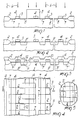
- Figure 1 illustrates an already intermediate structure obtained by means of standard steps comprising the definition or delimitation of the active regions on a P-type substrate 1 by growing field-oxide regions 2 which delimit said active regions. Said active regions are then subject, in a known manner, to a gate oxidation and to the subsequent deposition of a polysilicon layer which is then masked to shape the gate regions.
- the structure thus obtained has, besides the substrate 1 and the field oxide regions 2, the gate oxide layer 3 and the gate regions 4, and can be stored until requested by a final user indicating the required programming.
- the structure is subject to a gate-oxide etching to remove the portions of said layer which cover the active regions to the side of the gate regions 4.
- a masking step then follows to cover at least partially the memory cells which must be made permanently non-conductive.
- the resist regions 5 are superimposed at least partially on the gate regions and on the source and/or drain regions of the cells to be programmed.
- the resist mask 5 completely covers the gate region and the region of the substrate in which the drain of the memory cell should be produced, and only partially covers the substrate region corresponding to the source region, relatively to the second memory cell from the left of a row of the array, as illustrated in particular in figure 4.
- the other memory cells i.e.
- an annealing step is performed at 550°C to recover the crystallographic damage due to the implanting and to make electrically active the atoms of the source and drain regions respectively indicated by 7′ and 8′ in figure 2.
- the gate region of the second cell from the left is separated from the drain region 8′, which it would otherwise have in common with the adjacent leftward region, and from the common-source region 7′ which is shared with the adjacent rightward cell and with the cells located above and below in the same column in the layout of figure 4.
- the method continues conventionally by re-oxidating the source and drain regions, depositing the covering dielectric (indicated at 10 in figure 3), opening the contacts, providing the metalizations (the one provided at the drain contact 12 being shown in figure 3) and by subsequently performing passivation.
- Figure 3 also illustrates the region 11 at the drain contact, which is doped with phosphorus originating from a pre-deposition performed after opening the contacts in the dielectric.
- the programming masking can be performed simultaneously with the masking for implanting the source and drain regions of the transistors having the same channel type as the memory cells, typically the N-channel type.
- the production method comprises the conventional initial steps for defining the active regions, possibly implanting boron to adjust the threshold voltage, growing the gate-oxide layer, forming the gate regions of all the transistors including the memory cells and hence etching the gate-oxide regions in the active regions laterally to said gate regions.
- a specific protection mask is deposited, covering the entire memory cell array to allow implanting of drain-extension phosphorus on the logical part of the circuit.
- the mask for delimiting the source and drain regions for example of the N type, is deposited. Said mask covers all the P-channel transistors, part of the drain regions of the N-channel transistors with drain-extension in the logical part and part of the cells in the ROM array to be programmed, to prevent the source and/or drain regions of the cells which must be set permanently off to be implanted.
- This step corresponds (as regards the part of the circuit comprising the ROM memory) to the step illustrated in figure 1 and already explained earlier.
- a second mask is deposited to allow implanting of the source and drain regions of the P-channel transistors of the logical part.
- Said mask covers all the N-channel transistors in the logical portion and completely covers the array of memory cells (which are also of the N-channel type, as mentioned).
- the employed process entails no drain-extension transistors, the protection masking step and the subsequent phosphorus implanting are naturally eliminated, thus avoiding the addition of processing steps to the standard method.
- the memory cells which must be programmed so as to be permanently non-conductive are shielded during the source and drain implanting step to prevent the related source and/or drain region to form, or at least, when size or process reasons prevent this elimination, to provide a non-doped region to the side of the channel region extending below the gate, i.e. to widen the channel region beyond the gate region so as to prevent switching-on of the transistor constituting the memory cell when the related gate is biased.
- the mask must at least partially cover the substrate portion in which the source region should be provided or, as in the illustrated example, the substrate region in which the drain region should be provided.
- the optimum situation is to cover both regions to the side of the gate, eliminating or at least separating the source and drain regions from their own gate region.
- the dimensions of the device are critical to the point that they do not ensure safety conditions in the production of the memory array (for example in the production of common-source memory arrays of the type illustrated in figure 4, where however the source band 7 is very narrow, so that a misalignment of the programming mask may completely cover the common-source band, causing a production error)
- the protection mask may be designed, on the critical side, so as to cover only part of the gate region of the cell to be programmed.
- the programming mask preferably covers only the part of the gate directed towards the drain region (i.e. the leftward portion of the programmed cell) and said drain region, as shown in the detail illustrated in figure 5, where the programming mask has been indicated by 5′.
- the invention fully achieves the intended aim and objects.
- a programming method is provided which can be performed in a rather advanced step of the production process, since it is executed after forming the gate regions of the transistors.
- the method according to the invention entails programming in an apparently earlier step with respect to the known solution which implanted boron after forming the source and drain regions of all the memory cells, programming times are actually shorter than, or in any case comparable with, those of said known method, since the long oxidation step is eliminated.
- the described method is furthermore particularly suitable for processes involving low-resistivity polysilicon layer, since it eliminates the second oxidation which reduces the thickness of the polycrystalline silicon layer, increasing its resistivity.
- This method can furthermore be also applied to VLSI processes with thin gate oxide (under 350 ⁇ ) does not reduce the breakdown voltage of the junctions and is very reliable.
- a boron implanting can be introduced immediately ahead of the programming masking.
- This boron implanting which can be added to the threshold-adjustment boron implanting performed before gate oxidation, allows to form a heavily doped region with P-type conductivity laterally to the gate so as to prevent switching on of the channel.
Landscapes
- Semiconductor Memories (AREA)
- Read Only Memory (AREA)
Applications Claiming Priority (2)
| Application Number | Priority Date | Filing Date | Title |
|---|---|---|---|
| IT19989/88A IT1217372B (it) | 1988-03-28 | 1988-03-28 | Procedimento per la programmazione di memorie rom in tecnologia mos ecmos |
| IT1998988 | 1988-03-28 |
Publications (2)
| Publication Number | Publication Date |
|---|---|
| EP0335148A2 true EP0335148A2 (de) | 1989-10-04 |
| EP0335148A3 EP0335148A3 (de) | 1990-01-24 |
Family
ID=11162894
Family Applications (1)
| Application Number | Title | Priority Date | Filing Date |
|---|---|---|---|
| EP89104165A Withdrawn EP0335148A3 (de) | 1988-03-28 | 1989-03-09 | Verfahren zur Pragrammierung von MOS und CMOS-ROM-Speichern |
Country Status (4)
| Country | Link |
|---|---|
| US (1) | US5091329A (de) |
| EP (1) | EP0335148A3 (de) |
| JP (1) | JPH0210766A (de) |
| IT (1) | IT1217372B (de) |
Cited By (1)
| Publication number | Priority date | Publication date | Assignee | Title |
|---|---|---|---|---|
| FR2670316A1 (fr) * | 1990-12-10 | 1992-06-12 | Samsung Electronics Co Ltd | Procede de fabrication d'un dispositif de memoire morte a masque. |
Families Citing this family (8)
| Publication number | Priority date | Publication date | Assignee | Title |
|---|---|---|---|---|
| IT1239707B (it) * | 1990-03-15 | 1993-11-15 | St Microelectrics Srl | Processo per la realizzazione di una cella di memoria rom a bassa capacita' di drain |
| EP0575688B1 (de) * | 1992-06-26 | 1998-05-27 | STMicroelectronics S.r.l. | Programmierung von LDD-ROM-Zellen |
| US5380676A (en) * | 1994-05-23 | 1995-01-10 | United Microelectronics Corporation | Method of manufacturing a high density ROM |
| JPH08139208A (ja) * | 1994-11-04 | 1996-05-31 | Toyota Motor Corp | 不揮発性メモリの製造システム及びその製造方法 |
| US5538914A (en) * | 1995-08-03 | 1996-07-23 | Taiwan Semiconductor Manufacturing Company | LDD method of coding mask ROM device and LDD coded mask ROM device produced thereby |
| TW335537B (en) * | 1996-11-25 | 1998-07-01 | United Microelectronics Corp | The ROM unit and manufacture method |
| US6380016B2 (en) * | 1998-06-23 | 2002-04-30 | Ross Alan Kohler | Method for forming programmable CMOS ROM devices |
| KR100546360B1 (ko) | 2003-08-06 | 2006-01-26 | 삼성전자주식회사 | Nor형 마스크 rom 소자 및 이를 포함하는 반도체소자의 제조 방법 |
Family Cites Families (11)
| Publication number | Priority date | Publication date | Assignee | Title |
|---|---|---|---|---|
| JPS5529116A (en) * | 1978-08-23 | 1980-03-01 | Hitachi Ltd | Manufacture of complementary misic |
| US4406049A (en) * | 1980-12-11 | 1983-09-27 | Rockwell International Corporation | Very high density cells comprising a ROM and method of manufacturing same |
| EP0054102A3 (de) * | 1980-12-11 | 1983-07-27 | Rockwell International Corporation | ROM-Zellen in sehr dichter Anordnung und Herstellungsverfahren |
| US4359817A (en) * | 1981-05-28 | 1982-11-23 | General Motors Corporation | Method for making late programmable read-only memory devices |
| GB2102623B (en) * | 1981-06-30 | 1985-04-11 | Tokyo Shibaura Electric Co | Method of manufacturing a semiconductors memory device |
| US4536944A (en) * | 1982-12-29 | 1985-08-27 | International Business Machines Corporation | Method of making ROM/PLA semiconductor device by late stage personalization |
| US4536947A (en) * | 1983-07-14 | 1985-08-27 | Intel Corporation | CMOS process for fabricating integrated circuits, particularly dynamic memory cells with storage capacitors |
| US4683641A (en) * | 1983-08-01 | 1987-08-04 | Gte Communication Systems Corp. | Method of coding a MOS ROM array |
| US4598460A (en) * | 1984-12-10 | 1986-07-08 | Solid State Scientific, Inc. | Method of making a CMOS EPROM with independently selectable thresholds |
| US4642877A (en) * | 1985-07-01 | 1987-02-17 | Texas Instruments Incorporated | Method for making charge coupled device (CCD)-complementary metal oxide semiconductor (CMOS) devices |
| US4826779A (en) * | 1986-10-24 | 1989-05-02 | Teledyne Industries, Inc. | Integrated capacitor and method of fabricating same |
-
1988
- 1988-03-28 IT IT19989/88A patent/IT1217372B/it active
-
1989
- 1989-03-09 EP EP89104165A patent/EP0335148A3/de not_active Withdrawn
- 1989-03-13 US US07/322,132 patent/US5091329A/en not_active Expired - Lifetime
- 1989-03-27 JP JP1076386A patent/JPH0210766A/ja active Pending
Cited By (1)
| Publication number | Priority date | Publication date | Assignee | Title |
|---|---|---|---|---|
| FR2670316A1 (fr) * | 1990-12-10 | 1992-06-12 | Samsung Electronics Co Ltd | Procede de fabrication d'un dispositif de memoire morte a masque. |
Also Published As
| Publication number | Publication date |
|---|---|
| JPH0210766A (ja) | 1990-01-16 |
| US5091329A (en) | 1992-02-25 |
| IT1217372B (it) | 1990-03-22 |
| EP0335148A3 (de) | 1990-01-24 |
| IT8819989A0 (it) | 1988-03-28 |
Similar Documents
| Publication | Publication Date | Title |
|---|---|---|
| US6482698B2 (en) | Method of manufacturing an electrically programmable, non-volatile memory and high-performance logic circuitry in the same semiconductor chip | |
| US5793086A (en) | NOR-type ROM with LDD cells and process of fabrication | |
| JP4223551B2 (ja) | フローティングゲート不揮発性メモリデバイスの製造方法 | |
| US5610421A (en) | Integrated circuit with EPROM cells | |
| US6159795A (en) | Low voltage junction and high voltage junction optimization for flash memory | |
| JPS59124158A (ja) | Fetメモリ素子の形成方法 | |
| JPH10247725A5 (de) | ||
| US6730555B2 (en) | Transistors having selectively doped channel regions | |
| US5500392A (en) | Planar process using common alignment marks for well implants | |
| US6423589B2 (en) | Methods for fabricating CMOS integrated circuits including source/drain compensating regions | |
| US5385856A (en) | Manufacture of the fieldless split-gate EPROM/Flash EPROM | |
| US5696399A (en) | Process for manufacturing MOS-type integrated circuits | |
| US5091329A (en) | Method for programming mos and cmos rom memories | |
| US5545580A (en) | Multi-state read-only memory using multiple polysilicon selective depositions | |
| KR20010014742A (ko) | 반도체장치 및 그 제조방법 | |
| KR100546360B1 (ko) | Nor형 마스크 rom 소자 및 이를 포함하는 반도체소자의 제조 방법 | |
| EP1878057A2 (de) | Einmal programmierbarer schreibgeschützter speicher | |
| EP0914679A2 (de) | Herstellungsverfahren eines festwertspeichers der den epromprozess mit dem standard-cmos-prozess kombiniert | |
| EP0227965B1 (de) | Verfahren zum Programmieren durch Ionen-Implantation von Nurlesespeichern-NMOS und ein dadurch erhaltener Nurlesespeicher-NMOS | |
| US5372961A (en) | Method for manufacturing a semiconductor integrated circuit device | |
| EP1102319B1 (de) | Herstellungsverfahren für elektronische Bauelemente mit Hochspannungs-MOS- und EEPROM-Transistoren | |
| US6124169A (en) | Contact structure and associated process for production of semiconductor electronic devices and in particular nonvolatile EPROM and flash EPROM memories | |
| JPS62265765A (ja) | 半導体装置の製造方法 | |
| KR930000613B1 (ko) | 2중 폴리사이드 게이트 씨모스 제조방법 | |
| US5830772A (en) | Method for fabricating isolating regions for buried conductors |
Legal Events
| Date | Code | Title | Description |
|---|---|---|---|
| PUAI | Public reference made under article 153(3) epc to a published international application that has entered the european phase |
Free format text: ORIGINAL CODE: 0009012 |
|
| AK | Designated contracting states |
Kind code of ref document: A2 Designated state(s): DE FR GB NL SE |
|
| PUAL | Search report despatched |
Free format text: ORIGINAL CODE: 0009013 |
|
| AK | Designated contracting states |
Kind code of ref document: A3 Designated state(s): DE FR GB NL SE |
|
| STAA | Information on the status of an ep patent application or granted ep patent |
Free format text: STATUS: THE APPLICATION IS DEEMED TO BE WITHDRAWN |
|
| 18D | Application deemed to be withdrawn |
Effective date: 19900725 |