EP0334804A2 - Circuit résonnant à couplage de phase stabilisé - Google Patents
Circuit résonnant à couplage de phase stabilisé Download PDFInfo
- Publication number
- EP0334804A2 EP0334804A2 EP89730081A EP89730081A EP0334804A2 EP 0334804 A2 EP0334804 A2 EP 0334804A2 EP 89730081 A EP89730081 A EP 89730081A EP 89730081 A EP89730081 A EP 89730081A EP 0334804 A2 EP0334804 A2 EP 0334804A2
- Authority
- EP
- European Patent Office
- Prior art keywords
- phase
- phase shift
- frequency
- circuit
- oscillation
- Prior art date
- Legal status (The legal status is an assumption and is not a legal conclusion. Google has not performed a legal analysis and makes no representation as to the accuracy of the status listed.)
- Granted
Links
- 230000008878 coupling Effects 0.000 title description 2
- 238000010168 coupling process Methods 0.000 title description 2
- 238000005859 coupling reaction Methods 0.000 title description 2
- 230000005540 biological transmission Effects 0.000 claims abstract description 18
- 230000010355 oscillation Effects 0.000 claims abstract description 12
- 230000010363 phase shift Effects 0.000 claims abstract description 12
- 238000000034 method Methods 0.000 claims description 7
- 238000012546 transfer Methods 0.000 claims description 7
- 230000008859 change Effects 0.000 claims description 5
- 230000001427 coherent effect Effects 0.000 claims description 3
- 230000001419 dependent effect Effects 0.000 claims description 3
- 238000001514 detection method Methods 0.000 claims description 2
- 238000011156 evaluation Methods 0.000 claims 1
- 230000005291 magnetic effect Effects 0.000 description 13
- 230000001939 inductive effect Effects 0.000 description 8
- 230000008901 benefit Effects 0.000 description 3
- 238000012545 processing Methods 0.000 description 3
- 230000001105 regulatory effect Effects 0.000 description 3
- 239000003990 capacitor Substances 0.000 description 2
- 230000007613 environmental effect Effects 0.000 description 2
- 230000004907 flux Effects 0.000 description 2
- 230000008569 process Effects 0.000 description 2
- 230000009466 transformation Effects 0.000 description 2
- 241001136792 Alle Species 0.000 description 1
- 238000006424 Flood reaction Methods 0.000 description 1
- 230000009471 action Effects 0.000 description 1
- 230000002411 adverse Effects 0.000 description 1
- 230000032683 aging Effects 0.000 description 1
- 230000003321 amplification Effects 0.000 description 1
- 230000002457 bidirectional effect Effects 0.000 description 1
- 239000000969 carrier Substances 0.000 description 1
- 238000010276 construction Methods 0.000 description 1
- 230000007812 deficiency Effects 0.000 description 1
- 230000003111 delayed effect Effects 0.000 description 1
- 230000000501 effect on contamination Effects 0.000 description 1
- 230000000694 effects Effects 0.000 description 1
- 238000005516 engineering process Methods 0.000 description 1
- 238000003780 insertion Methods 0.000 description 1
- 230000037431 insertion Effects 0.000 description 1
- 230000010354 integration Effects 0.000 description 1
- 239000006249 magnetic particle Substances 0.000 description 1
- 230000007257 malfunction Effects 0.000 description 1
- 238000004519 manufacturing process Methods 0.000 description 1
- 238000003199 nucleic acid amplification method Methods 0.000 description 1
- 230000000704 physical effect Effects 0.000 description 1
- 230000002441 reversible effect Effects 0.000 description 1
- 230000008054 signal transmission Effects 0.000 description 1
- 230000003068 static effect Effects 0.000 description 1
- 230000001360 synchronised effect Effects 0.000 description 1
- 238000013519 translation Methods 0.000 description 1
- 229910000859 α-Fe Inorganic materials 0.000 description 1
Images


Classifications
-
- H—ELECTRICITY
- H04—ELECTRIC COMMUNICATION TECHNIQUE
- H04B—TRANSMISSION
- H04B5/00—Near-field transmission systems, e.g. inductive or capacitive transmission systems
- H04B5/20—Near-field transmission systems, e.g. inductive or capacitive transmission systems characterised by the transmission technique; characterised by the transmission medium
- H04B5/22—Capacitive coupling
-
- G—PHYSICS
- G06—COMPUTING; CALCULATING OR COUNTING
- G06K—GRAPHICAL DATA READING; PRESENTATION OF DATA; RECORD CARRIERS; HANDLING RECORD CARRIERS
- G06K7/00—Methods or arrangements for sensing record carriers, e.g. for reading patterns
- G06K7/10—Methods or arrangements for sensing record carriers, e.g. for reading patterns by electromagnetic radiation, e.g. optical sensing; by corpuscular radiation
- G06K7/10009—Methods or arrangements for sensing record carriers, e.g. for reading patterns by electromagnetic radiation, e.g. optical sensing; by corpuscular radiation sensing by radiation using wavelengths larger than 0.1 mm, e.g. radio-waves or microwaves
- G06K7/10316—Methods or arrangements for sensing record carriers, e.g. for reading patterns by electromagnetic radiation, e.g. optical sensing; by corpuscular radiation sensing by radiation using wavelengths larger than 0.1 mm, e.g. radio-waves or microwaves using at least one antenna particularly designed for interrogating the wireless record carriers
- G06K7/10336—Methods or arrangements for sensing record carriers, e.g. for reading patterns by electromagnetic radiation, e.g. optical sensing; by corpuscular radiation sensing by radiation using wavelengths larger than 0.1 mm, e.g. radio-waves or microwaves using at least one antenna particularly designed for interrogating the wireless record carriers the antenna being of the near field type, inductive coil
-
- Y—GENERAL TAGGING OF NEW TECHNOLOGICAL DEVELOPMENTS; GENERAL TAGGING OF CROSS-SECTIONAL TECHNOLOGIES SPANNING OVER SEVERAL SECTIONS OF THE IPC; TECHNICAL SUBJECTS COVERED BY FORMER USPC CROSS-REFERENCE ART COLLECTIONS [XRACs] AND DIGESTS
- Y02—TECHNOLOGIES OR APPLICATIONS FOR MITIGATION OR ADAPTATION AGAINST CLIMATE CHANGE
- Y02D—CLIMATE CHANGE MITIGATION TECHNOLOGIES IN INFORMATION AND COMMUNICATION TECHNOLOGIES [ICT], I.E. INFORMATION AND COMMUNICATION TECHNOLOGIES AIMING AT THE REDUCTION OF THEIR OWN ENERGY USE
- Y02D30/00—Reducing energy consumption in communication networks
- Y02D30/70—Reducing energy consumption in communication networks in wireless communication networks
Definitions
- the invention relates to a contactless energy and data transmission system consisting of a micro station, hereinafter referred to as MS, and a micro unit, hereinafter referred to as ME.
- data carriers and data devices are e.g. used in the form of chip cards with integrated electronic components.
- Almost all systems available on the market are designed with contacts between the reader and the card. Contacts have an adverse effect on contamination, static discharges, vibrations and wear.
- a transmission frequency such that clock signals can be used on the ME side to operate the electronic modules used in the ME, which are the same as the transmission frequency or can be obtained indirectly from it by subdivision.
- the frequency used should comply with international guidelines and standards. The frequency used must therefore be kept constant. This contradicts the change (aging, component tolerance) of components that are used in the resonant circuit to generate the transmission oscillation, so that with such changed component parameters, the natural frequency of the resonant circuit no longer corresponds to the control frequency and thus the energy translation from MS to ME is reduced.
- Another condition is that two resonant circuits must be set up, which, for reasons of unambiguous signal detection on the part of the ME, must have a constant phase relationship to one another.
- the inductive transmission path of this system is divided into the main features: - energy transfer - control loop - Magnetic stripe compatibility - data transfer - Layer variance - clock generation
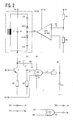
- the energy is processed in two frequency-coupled resonant circuits (Figure 1: T1, S1 and T2, S2) at a frequency of 6 MHz, for example.
- the ferrite core coils of the resonant circuits contain an air slot into which the respective flat coils S3 and S4 of the ME are inserted.
- the magnetic flux is therefore perpendicular to the flat coils.
- the two resonant circuits work against each other with a regulated phase shift of +/- 90 °.
- resonant circuits have the advantage that relatively little energy is required to operate the system if it is very selective and with resonance peaks, i.e. work near the natural resonance.
- each circuit S1 and S2 is constructed in an independent control circuit of the same frequency.
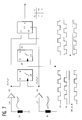
- Figure 2 shows the basic structure of the control loop.
- the control circuit takes advantage of the physical property of the resonant circuit, that in the desired resonance case the circuit S1 / S2, Figure 2, acts exclusively as a real resistance.
- the phase position of the voltages between the collector and the base of the driver transistor T, Figure 2 is exactly 180 °.
- the phase position of the circle is tapped with the voltage Uc.
- This reference signal Up required for a channel, e.g. Q2 ( Figure 1) is used by the other channel, e.g. Q3 ( Figure 1), which is used to use coherent signal curves for control. This ensures that both resonant circuits maintain the same frequency with constant phase shift.
- the capacitors C11 and C12 work as voltage dividers so that the permissible reverse voltage of the series-connected capacitance diodes KD11 and KD12 ( Figure 2) is not exceeded.
- the controller presented in Figure 2 is built up twice for circuits S1, T1 and S2, T2 ( Figure 1).
- the capacitive portion in the resonant circuit is said to have increased.
- the natural resonance frequency of the individual circuit with coil and capacitor drops.
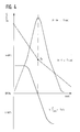
- the driver specifies a fixed frequency from the outside, the phase and thus also the amplitude change (see Figure 4).
- the phase of the voltage Ux will lag behind the voltage Up by more than 90 ° phase difference (case B, Figure 3).
- the mean value of the signal Uf (Un) increases.
- control loop implemented according to Figure 2 contained an additional function that is necessary because the circuit S2 ( Figure 1) experiences phase changes of 180 ° through the exclusive-OR gate "5" with the data to be transmitted to the ME.
- stage T2, S2 is the same as stage T1, S1, ( Figure 1) with one exception.
- stages T2, S2 are operated with the phase-switchable signal TM2.
- the reference phase for the comparison in the EXCLUSIVE-OR gate U1 is obtained from Q2.
- the magnetic coding on the magnetic stripe is not affected.
- This property is due to the fact that the magnetic flux with a frequency f> 1 MHz floods the card vertically. Due to their inertia and direction, the magnetic particles of the magnetic strip have no way of changing their position.
- the two resonant circuits work with a phase difference of +/- 90 °.
- the resonant circuit S1 In the idle state (no data transmission), the resonant circuit S1 is always 90 ° ahead of the resonant circuit S2.
- S2 In the case of data transmission to the microunit, S2 is switched by 180 °, so that it is then 90 ° ahead of circuit S1. This process is evaluated by the ME.
- a data transmission from the ME to the MS occurs due to an increased current consumption by the ME.
- a voltage drop can be detected via the internal resistance of the source in the micro station. This method is described by the patent (No. P344756.05).
- the function of the system is not dependent on the position of the ME in the receiving device.
- the 2 required coils of the ME and MS were attached to the chip card system, as shown in Figure 6 (see utility model application no. G 8716548.1). This ensures that, irrespective of how the ME was rotated before being introduced into the receiving device of the MS, the 2 coils of the ME are opposite to the 2 coils of the MS, whereby the function is always guaranteed and the handling of the system is simplified.
- An arithmetic unit, microcomputer, etc. can be accommodated on the microunit.
- the required processing cycle is obtained directly or divided from the frequency of the energy transfer (see Figure 7).
- U3 and U4 derive a digital signal from the sinusoidal analog voltage of the receiver coils. No separate oscillator is required for the microunit, which contributes to the significant simplification of the ME.
- the basic prerequisite for the correct operation of an arithmetic unit in an ME is that the processing cycle is available symmetrically and without irregularities. Since the ME should work in any insertion position in the MS, care must be taken that the clock is removed from the non-modulated coil ( Figure 6).
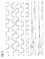
- Case 1 and Case 2 show the different signal curves in different operating positions (see also Figure 6).
- Case 1 shows that U3 is ahead of U4: The phase modulation takes place later on U4. The clock is obtained from U3.
- Case 2 shows that U4 is ahead of U3: The phase modulation takes place later on U3. The clock is obtained from U4.
- the flip-flop U5 recognizes a logic "1" for case 1 and a logic “0" for case 2 at the output. Slightly delayed when the operating voltage of the ME has built up and a delay time of a few microseconds has elapsed, there is a positive one Reset edge on flip-flop U6. See also picture 5.
- This process only happens once at the start of operation if no data has yet been transferred.
- the level and basic state of the data line DR ( Figure 7) are determined according to the same principle of clock assignment, with the difference that the data signal is only defined for this level and no multiplexer is required.
Landscapes
- Engineering & Computer Science (AREA)
- Computer Networks & Wireless Communication (AREA)
- Health & Medical Sciences (AREA)
- Toxicology (AREA)
- Physics & Mathematics (AREA)
- Electromagnetism (AREA)
- General Health & Medical Sciences (AREA)
- Artificial Intelligence (AREA)
- Computer Vision & Pattern Recognition (AREA)
- General Physics & Mathematics (AREA)
- Theoretical Computer Science (AREA)
- Signal Processing (AREA)
- Near-Field Transmission Systems (AREA)
- Inductance-Capacitance Distribution Constants And Capacitance-Resistance Oscillators (AREA)
Applications Claiming Priority (2)
| Application Number | Priority Date | Filing Date | Title |
|---|---|---|---|
| DE3810702 | 1988-03-25 | ||
| DE3810702A DE3810702A1 (de) | 1988-03-25 | 1988-03-25 | Phasenstabilisierter, -gekoppelter schwingkreis |
Publications (3)
| Publication Number | Publication Date |
|---|---|
| EP0334804A2 true EP0334804A2 (fr) | 1989-09-27 |
| EP0334804A3 EP0334804A3 (en) | 1990-05-16 |
| EP0334804B1 EP0334804B1 (fr) | 1994-11-02 |
Family
ID=6350997
Family Applications (1)
| Application Number | Title | Priority Date | Filing Date |
|---|---|---|---|
| EP89730081A Expired - Lifetime EP0334804B1 (fr) | 1988-03-25 | 1989-03-22 | Circuit résonnant à couplage de phase stabilisé |
Country Status (4)
| Country | Link |
|---|---|
| US (1) | US4928087A (fr) |
| EP (1) | EP0334804B1 (fr) |
| JP (1) | JPH01311391A (fr) |
| DE (2) | DE3810702A1 (fr) |
Cited By (8)
| Publication number | Priority date | Publication date | Assignee | Title |
|---|---|---|---|---|
| FR2670642A1 (fr) * | 1990-12-18 | 1992-06-19 | Adventure | Systeme de transmission de donnees a alimentation des moyens d'emission d'un emetteur par un recepteur. |
| EP0509125A1 (fr) * | 1991-04-19 | 1992-10-21 | Siemens Aktiengesellschaft | Dispositif pour la transmission sans contact de données et d'énergie et procédé de mise en oeuvre |
| WO1993023908A1 (fr) * | 1992-05-10 | 1993-11-25 | Auckland Uniservices Limited | Systeme de distribution d'energie depourvu de contact |
| EP0644681A2 (fr) * | 1993-08-15 | 1995-03-22 | Angewandte Digital Elektronik GmbH | Carte avec verrouillage dans le cas d'une interrogation à distance |
| NL9301697A (nl) * | 1993-10-01 | 1995-05-01 | Nedap Nv | Fasedemodulator voor contactloze chipkaarten. |
| EP0704814A3 (fr) * | 1994-09-30 | 1997-06-04 | Toshiba Kk | Système d'excitation de circuits à couplage magnétique |
| EP0984402A3 (fr) * | 1998-08-31 | 2004-06-02 | Citicorp Development Center, Inc. | Terminal pour cartes à valeur mémorisée |
| CN107735923A (zh) * | 2015-06-04 | 2018-02-23 | 富士通株式会社 | 受电器以及电力传输系统 |
Families Citing this family (22)
| Publication number | Priority date | Publication date | Assignee | Title |
|---|---|---|---|---|
| US5327122A (en) * | 1989-09-04 | 1994-07-05 | Massimo Casalegno | Installation for data transmission with correction of phase error |
| DE59010221D1 (de) * | 1990-07-16 | 1996-04-25 | Siemens Ag | Einrichtung zur berührungslosen Daten- und Energieübertragung sowie Verwendung einer solchen |
| DE4107311C2 (de) * | 1991-03-07 | 1996-02-08 | Telefunken Microelectron | Verfahren zur drahtlosen Übertragung von Daten auf einen Datenträger |
| DE4125143C5 (de) * | 1991-07-30 | 2004-07-01 | Ulrich Dr.-Ing. Schwan | Einrichtung zur kontaktlosen Übertragung von Wechselsignalen |
| JP2659315B2 (ja) * | 1992-11-13 | 1997-09-30 | 株式会社ピーエフユー | 非接触型icメモリカードシステム |
| EP0601739B1 (fr) * | 1992-11-25 | 2001-05-30 | Simmonds Precision Products Inc. | Structure et procédé de traitement de données |
| DE4326213C1 (de) * | 1993-08-04 | 1994-08-18 | Siemens Ag | Einrichtung zur berührungslosen Signal- und Energieübertragung |
| FR2711440B1 (fr) * | 1993-10-18 | 1996-02-02 | France Telecom | Dispositif à pureté spectrale pour l'échange d'informations à distance entre un objet portatif et une station. |
| DE4438286C2 (de) * | 1994-10-26 | 2002-09-12 | Siemens Ag | System zur kontaktlosen Energie- und Datenübertragung |
| DE4438287C1 (de) * | 1994-10-26 | 1996-05-09 | Siemens Ag | System zur kontaktlosen Energie- und Datenübertragung |
| DE19621076C2 (de) * | 1996-05-24 | 2001-06-28 | Siemens Ag | Vorrichtung und Verfahren zum kontaktlosen Übertragen von Energie oder Daten |
| DE19653522A1 (de) * | 1996-12-20 | 1998-06-25 | Bayerische Motoren Werke Ag | Verfahren zum drahtlosen Übertragen von Energie und Daten |
| DE19726335C2 (de) | 1997-06-20 | 2000-03-02 | Angewandte Digital Elektronik | Chipkarte mit mindestens zwei Spulenanordnungen zur Übertragung von Daten und/oder Energie |
| FR2780222B1 (fr) * | 1998-06-18 | 2000-08-11 | Sgs Thomson Microelectronics | Procede et systeme de detection par couplage inductif d'un signal de modulation de charge |
| DE10026175C2 (de) * | 2000-04-18 | 2003-02-27 | Schleifring Und Appbau Gmbh | Anordnung zur kontaktlosen Übertragung elektrischer Signale bzw. Energie zwischen einer feststehenden Einheit und mehreren ortsveränderlichen Einheiten |
| DE10158442B4 (de) * | 2001-12-01 | 2004-11-25 | Atmel Germany Gmbh | Sende- und Empfangseinrichtung für eine kontaktlose Datenübertragung |
| DE102007060811A1 (de) | 2007-09-01 | 2009-03-05 | Maquet Gmbh & Co. Kg | Vorrichtung und Verfahren zur drahtlosen Energie- und/oder Datenübertragung zwischen einem Quellgerät und mindestens einem Zielgerät |
| EP2031731A1 (fr) | 2007-09-01 | 2009-03-04 | MAQUET GmbH & Co. KG | Dispositif et procédé de transmission d'énergie et/ou de données sans fil entre un appareil source et au moins un appareil cible |
| US7999414B2 (en) | 2007-09-01 | 2011-08-16 | Maquet Gmbh & Co. Kg | Apparatus and method for wireless energy and/or data transmission between a source device and at least one target device |
| DE102008056927A1 (de) | 2007-11-19 | 2009-06-04 | Brühn, Xenia | Drahtlose Energie und Datenübertragung |
| US7876085B2 (en) * | 2009-06-10 | 2011-01-25 | Grenergy Opto, Inc. | Quasi-resonant valley voltage detecting method and apparatus |
| DE102012109359A1 (de) * | 2012-10-02 | 2014-04-03 | Infineon Technologies Ag | Booster-Antenne für eine Chip-Anordnung, Kontaktlos-Chipkartenmodul-Anordnung und Chip-Anordnung |
Citations (2)
| Publication number | Priority date | Publication date | Assignee | Title |
|---|---|---|---|---|
| EP0185610A2 (fr) * | 1984-12-21 | 1986-06-25 | Angewandte Digital Elektronik GmbH | Dispositif pour la transmission sans contact de signal et d'énergie |
| GB2173623A (en) * | 1985-04-10 | 1986-10-15 | The General Electric Co Plc | Transaction system |
Family Cites Families (3)
| Publication number | Priority date | Publication date | Assignee | Title |
|---|---|---|---|---|
| AU564509B2 (en) * | 1984-10-09 | 1987-08-13 | X-Cyte Inc. | Phase-encoded transponder interrogation |
| US4857893A (en) * | 1986-07-18 | 1989-08-15 | Bi Inc. | Single chip transponder device |
| IL82025A (en) * | 1987-03-27 | 1993-07-08 | Galil Electro Ltd | Electronic data communications system |
-
1988
- 1988-03-25 DE DE3810702A patent/DE3810702A1/de active Granted
-
1989
- 1989-03-22 EP EP89730081A patent/EP0334804B1/fr not_active Expired - Lifetime
- 1989-03-22 DE DE58908575T patent/DE58908575D1/de not_active Expired - Fee Related
- 1989-03-27 US US07/329,309 patent/US4928087A/en not_active Expired - Lifetime
- 1989-03-27 JP JP1072054A patent/JPH01311391A/ja active Pending
Patent Citations (2)
| Publication number | Priority date | Publication date | Assignee | Title |
|---|---|---|---|---|
| EP0185610A2 (fr) * | 1984-12-21 | 1986-06-25 | Angewandte Digital Elektronik GmbH | Dispositif pour la transmission sans contact de signal et d'énergie |
| GB2173623A (en) * | 1985-04-10 | 1986-10-15 | The General Electric Co Plc | Transaction system |
Cited By (12)
| Publication number | Priority date | Publication date | Assignee | Title |
|---|---|---|---|---|
| FR2670642A1 (fr) * | 1990-12-18 | 1992-06-19 | Adventure | Systeme de transmission de donnees a alimentation des moyens d'emission d'un emetteur par un recepteur. |
| EP0509125A1 (fr) * | 1991-04-19 | 1992-10-21 | Siemens Aktiengesellschaft | Dispositif pour la transmission sans contact de données et d'énergie et procédé de mise en oeuvre |
| US5329274A (en) * | 1991-04-19 | 1994-07-12 | Siemens Aktiengesellschaft | Apparatus for contactless data and energy transmission and method for operating such an apparatus |
| WO1993023908A1 (fr) * | 1992-05-10 | 1993-11-25 | Auckland Uniservices Limited | Systeme de distribution d'energie depourvu de contact |
| EP0644681A2 (fr) * | 1993-08-15 | 1995-03-22 | Angewandte Digital Elektronik GmbH | Carte avec verrouillage dans le cas d'une interrogation à distance |
| EP0644681A3 (fr) * | 1993-08-15 | 1995-08-23 | Angewandte Digital Elektronik | Carte avec verrouillage dans le cas d'une interrogation à distance. |
| NL9301697A (nl) * | 1993-10-01 | 1995-05-01 | Nedap Nv | Fasedemodulator voor contactloze chipkaarten. |
| EP0651539A1 (fr) * | 1993-10-01 | 1995-05-03 | N.V. Nederlandsche Apparatenfabriek NEDAP | Système de transmission d'informations sans contact modulée en phase |
| EP0704814A3 (fr) * | 1994-09-30 | 1997-06-04 | Toshiba Kk | Système d'excitation de circuits à couplage magnétique |
| EP0984402A3 (fr) * | 1998-08-31 | 2004-06-02 | Citicorp Development Center, Inc. | Terminal pour cartes à valeur mémorisée |
| CN107735923A (zh) * | 2015-06-04 | 2018-02-23 | 富士通株式会社 | 受电器以及电力传输系统 |
| CN107735923B (zh) * | 2015-06-04 | 2021-02-05 | 富士通株式会社 | 受电器以及电力传输系统 |
Also Published As
| Publication number | Publication date |
|---|---|
| US4928087A (en) | 1990-05-22 |
| DE3810702C2 (fr) | 1992-01-02 |
| JPH01311391A (ja) | 1989-12-15 |
| DE3810702A1 (de) | 1989-10-12 |
| EP0334804A3 (en) | 1990-05-16 |
| DE58908575D1 (de) | 1994-12-08 |
| EP0334804B1 (fr) | 1994-11-02 |
Similar Documents
| Publication | Publication Date | Title |
|---|---|---|
| EP0334804B1 (fr) | Circuit résonnant à couplage de phase stabilisé | |
| DE2748584C2 (de) | Tragbares Detektierplättchen für eine Identifizierungsvorrichtung | |
| EP0788637B1 (fr) | Systeme pour la transmission d'energie et de donnees sans contact | |
| EP0473569B2 (fr) | Système de transmission de données par voie inductive sans contact | |
| EP0609875B1 (fr) | Méthode pour limiter la fréquence d'un oscillateur commandé en tension dans un circuit de contrÔle dans une alimentation de puissance avec un convertisseur résonant et circuit de contrÔle pour une alimentation de puissance avec un convertisseur résonant | |
| EP0510220B1 (fr) | Dispositif de transmission d'énergie et de données sans contact | |
| EP0245196B1 (fr) | Méthode de transmission de données entre une partie fixe et une partie mobile | |
| DE60312208T2 (de) | Abstimmbare antennenschaltung, insbesondere für ein kontaktloses integriertes lesegerät | |
| WO1996013792A1 (fr) | Systeme pour la transmission d'energie et d'information sans contact | |
| DE69232627T2 (de) | Verfahren zur kontaktfreien Kommunikation zwischen einem Halbleiter- Datenaufzeichnungsträger und einer Lese-/Schreibvorrichtung | |
| DE69922587T2 (de) | Übertragungsverfahren | |
| WO1986001058A1 (fr) | Installation pour le transfert de donnees binaires entre un support d'information mobile et une station fixe | |
| WO2015052033A1 (fr) | Circuit d'attaque pour bobine d'inductance, procédé permettant de faire fonctionner une bobine d'inductance et dispositif actif d'émission pourvu d'un circuit d'attaque | |
| EP0509125B1 (fr) | Dispositif pour la transmission sans contact de données et d'énergie et procédé de mise en oeuvre | |
| DE10345497B4 (de) | Oszillatorschaltung, insbesondere für den Mobilfunk | |
| EP2141637B1 (fr) | Support de données portatif doté d'une interface sans contact active et procédé de fonctionnement | |
| EP1110300B1 (fr) | Dispositif d'alimentation en courant et circuit associe a ce dispositif | |
| WO2004032040A1 (fr) | Support de donnees sans contact | |
| EP2340512B1 (fr) | Unité transpondeur | |
| EP0977144A1 (fr) | Porteur de données comportant une source de signal d'horloge verrouillable et méthode pour la production d'un signal d'horloge pour un porteur de données | |
| DE3524768A1 (de) | Anordnung zur synchronisation der pulsbreitenmodulierten schalttakte mehrerer getakteter gleichspannungswandler | |
| DD252935A1 (de) | Schaltungsanordnung zum synchronen anschwingen eines quarzstabilisierten generators | |
| EP0637877A1 (fr) | Dispositif de transfert sans contact de signaux et d'énergie | |
| DE3625270C2 (fr) | ||
| DE2357500C3 (de) | Schaltung zum Speichern des Zustandes eines Binärzählers bei Betriebsspannungsausfall |
Legal Events
| Date | Code | Title | Description |
|---|---|---|---|
| PUAI | Public reference made under article 153(3) epc to a published international application that has entered the european phase |
Free format text: ORIGINAL CODE: 0009012 |
|
| AK | Designated contracting states |
Kind code of ref document: A2 Designated state(s): CH DE FR GB IT LI |
|
| PUAL | Search report despatched |
Free format text: ORIGINAL CODE: 0009013 |
|
| AK | Designated contracting states |
Kind code of ref document: A3 Designated state(s): CH DE FR GB IT LI |
|
| 17P | Request for examination filed |
Effective date: 19900518 |
|
| 17Q | First examination report despatched |
Effective date: 19920811 |
|
| RAP1 | Party data changed (applicant data changed or rights of an application transferred) |
Owner name: ANGEWANDTE DIGITAL ELEKTRONIK GMBH |
|
| GRAA | (expected) grant |
Free format text: ORIGINAL CODE: 0009210 |
|
| AK | Designated contracting states |
Kind code of ref document: B1 Designated state(s): CH DE FR GB IT LI |
|
| PG25 | Lapsed in a contracting state [announced via postgrant information from national office to epo] |
Ref country code: IT Free format text: LAPSE BECAUSE OF FAILURE TO SUBMIT A TRANSLATION OF THE DESCRIPTION OR TO PAY THE FEE WITHIN THE PRE;WARNING: LAPSES OF ITALIAN PATENTS WITH EFFECTIVE DATE BEFORE 2007 MAY HAVE OCCURRED AT ANY TIME BEFORE 2007. THE CORRECT EFFECTIVE DATE MAY BE DIFFERENT FROM THE ONE RECORDED.SCRIBED TIME-LIMIT Effective date: 19941102 |
|
| GBT | Gb: translation of ep patent filed (gb section 77(6)(a)/1977) |
Effective date: 19941108 |
|
| REF | Corresponds to: |
Ref document number: 58908575 Country of ref document: DE Date of ref document: 19941208 |
|
| ET | Fr: translation filed | ||
| PLBE | No opposition filed within time limit |
Free format text: ORIGINAL CODE: 0009261 |
|
| STAA | Information on the status of an ep patent application or granted ep patent |
Free format text: STATUS: NO OPPOSITION FILED WITHIN TIME LIMIT |
|
| 26N | No opposition filed | ||
| PGFP | Annual fee paid to national office [announced via postgrant information from national office to epo] |
Ref country code: FR Payment date: 20000316 Year of fee payment: 12 Ref country code: GB Payment date: 20000316 Year of fee payment: 12 |
|
| PGFP | Annual fee paid to national office [announced via postgrant information from national office to epo] |
Ref country code: CH Payment date: 20000522 Year of fee payment: 12 |
|
| PGFP | Annual fee paid to national office [announced via postgrant information from national office to epo] |
Ref country code: DE Payment date: 20001205 Year of fee payment: 12 |
|
| PG25 | Lapsed in a contracting state [announced via postgrant information from national office to epo] |
Ref country code: GB Free format text: LAPSE BECAUSE OF NON-PAYMENT OF DUE FEES Effective date: 20010322 |
|
| PG25 | Lapsed in a contracting state [announced via postgrant information from national office to epo] |
Ref country code: LI Free format text: LAPSE BECAUSE OF NON-PAYMENT OF DUE FEES Effective date: 20010331 Ref country code: CH Free format text: LAPSE BECAUSE OF NON-PAYMENT OF DUE FEES Effective date: 20010331 |
|
| GBPC | Gb: european patent ceased through non-payment of renewal fee |
Effective date: 20010322 |
|
| REG | Reference to a national code |
Ref country code: CH Ref legal event code: PL |
|
| PG25 | Lapsed in a contracting state [announced via postgrant information from national office to epo] |
Ref country code: FR Free format text: LAPSE BECAUSE OF NON-PAYMENT OF DUE FEES Effective date: 20011130 |
|
| REG | Reference to a national code |
Ref country code: FR Ref legal event code: ST |
|
| PG25 | Lapsed in a contracting state [announced via postgrant information from national office to epo] |
Ref country code: DE Free format text: LAPSE BECAUSE OF NON-PAYMENT OF DUE FEES Effective date: 20020101 |