EP0333494B1 - Semiconductor driver for producing switching and offset signals - Google Patents
Semiconductor driver for producing switching and offset signals Download PDFInfo
- Publication number
- EP0333494B1 EP0333494B1 EP89302641A EP89302641A EP0333494B1 EP 0333494 B1 EP0333494 B1 EP 0333494B1 EP 89302641 A EP89302641 A EP 89302641A EP 89302641 A EP89302641 A EP 89302641A EP 0333494 B1 EP0333494 B1 EP 0333494B1
- Authority
- EP
- European Patent Office
- Prior art keywords
- voltage
- power supply
- fet
- field effect
- terminal
- Prior art date
- Legal status (The legal status is an assumption and is not a legal conclusion. Google has not performed a legal analysis and makes no representation as to the accuracy of the status listed.)
- Expired - Lifetime
Links
Images

Classifications
-
- H—ELECTRICITY
- H01—ELECTRIC ELEMENTS
- H01S—DEVICES USING THE PROCESS OF LIGHT AMPLIFICATION BY STIMULATED EMISSION OF RADIATION [LASER] TO AMPLIFY OR GENERATE LIGHT; DEVICES USING STIMULATED EMISSION OF ELECTROMAGNETIC RADIATION IN WAVE RANGES OTHER THAN OPTICAL
- H01S5/00—Semiconductor lasers
- H01S5/04—Processes or apparatus for excitation, e.g. pumping, e.g. by electron beams
- H01S5/042—Electrical excitation ; Circuits therefor
-
- H—ELECTRICITY
- H01—ELECTRIC ELEMENTS
- H01S—DEVICES USING THE PROCESS OF LIGHT AMPLIFICATION BY STIMULATED EMISSION OF RADIATION [LASER] TO AMPLIFY OR GENERATE LIGHT; DEVICES USING STIMULATED EMISSION OF ELECTROMAGNETIC RADIATION IN WAVE RANGES OTHER THAN OPTICAL
- H01S5/00—Semiconductor lasers
- H01S5/02—Structural details or components not essential to laser action
- H01S5/026—Monolithically integrated components, e.g. waveguides, monitoring photo-detectors, drivers
-
- H—ELECTRICITY
- H03—ELECTRONIC CIRCUITRY
- H03K—PULSE TECHNIQUE
- H03K17/00—Electronic switching or gating, i.e. not by contact-making and –breaking
- H03K17/04—Modifications for accelerating switching
- H03K17/041—Modifications for accelerating switching without feedback from the output circuit to the control circuit
- H03K17/04106—Modifications for accelerating switching without feedback from the output circuit to the control circuit in field-effect transistor switches
-
- H—ELECTRICITY
- H03—ELECTRONIC CIRCUITRY
- H03K—PULSE TECHNIQUE
- H03K17/00—Electronic switching or gating, i.e. not by contact-making and –breaking
- H03K17/08—Modifications for protecting switching circuit against overcurrent or overvoltage
- H03K17/081—Modifications for protecting switching circuit against overcurrent or overvoltage without feedback from the output circuit to the control circuit
- H03K17/0814—Modifications for protecting switching circuit against overcurrent or overvoltage without feedback from the output circuit to the control circuit by measures taken in the output circuit
- H03K17/08142—Modifications for protecting switching circuit against overcurrent or overvoltage without feedback from the output circuit to the control circuit by measures taken in the output circuit in field-effect transistor switches
Definitions
- the present invention relates to a semiconductor integrated circuit device for driving an external load such as a laser diode, and more specifically relates to a semiconductor integrated circuit device of the GaAs digital IC type having a GaAs substrate formed thereon with a plurality of Shottky junction type field effect transistors.
- the GaAs digital IC becomes more important for use as a semiconductor laser driver (hereinafter, referred to as "laser driver") for driving directly a semiconductor laser at an ultra high speed (c.f. Japanese Electrocommunication Society, technology research report SSD-85-140), and The Technical Digest of the IEEE GaAs IC Symposium 1985 pages 103-106 which discloses a GaAs laser-driver operating at up to 2 Gbits/s data rate.
- laser driver semiconductor laser driver
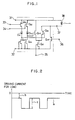
- Fig. 1 shows a driver described in the above-mentioned document, constructed of field effect transistors (FETs) and diodes which are composed of Shottky junction type field effect transistors and diodes. These FETs and diodes are formed on a GaAs substrate together with other components.
- FETs field effect transistors
- diodes which are composed of Shottky junction type field effect transistors and diodes.
- the laser driver is provided with an earth terminal 31 and a power supply terminal 32. Normally, a power supply voltage of -5.2V is applied to the power supply terminal 32 with respect to the earth terminal 31.
- An input signal is inputted from an input terminal 33 through a level shifting circuit comprised of FET Q41, level shifting diode D41 and current supplying FET Q43 into a gate electrode of FET Q46 which constitutes a part of output differentially operating circuit.
- the laser driver is provided with a reference terminal 34 receptive of a reference signal such as an opposite phase signal or a reference voltage of -1.3V.
- the reference signal received at the reference terminal 34 is inputted through another level shifting circuit composed of FET Q42, level shifting diode D42 and current supplying FET Q44 into a gate electrode of FET Q45 which is contained in the output differentially operating circuit.
- the output differentially operating circuit is comprised of the FET Q45, the FET Q46 and current supplying FET Q47, and carries out switching of an output current at ultra high speed.
- the gate electrode of FET Q47 is connected.to a switching current control terminal 35, and the drain terminal of FET Q46 is connected to an output terminal 37.
- an FET Q48 has a function of supplying an offset current, and the gate electrode thereof is connected to an offset current control terminal 36 and the drain terminal thereof is connected to the output terminal 37.
- the drain current flowing through the FET Q48 is applied to a load in the form of a laser diode 38 as an offset current I o
- the drain current flowing through the FET Q47 included in the output differentially operating circuit is also applied to the load as a switching current I s .
- the offset current I o can be controlled by applying externally a control voltage to the offset current control terminal 36
- the switching current I s can be controlled by applying externally another control voltage to the switching current control terminal 35.
- a needed maximum value of the switching current I s is about 50mA
- a needed variable range of the offset current I o is from 0mA to 100mA.
- the set value of offset current I o is determined according to a threshold current of the laser diode 38.
- Fig. 2 shows the relation between the above-described offset current I o and switching current I s .
- a waveform a represents a time-responsive waveform of the output current where the magnitude of offset current I o is indicated by b , and the amplitude of switching current I s is indicated by c .
- the threshold value V th is set within the range from about -1.0V to about -0.5V for the high speed operation.
- a high performance FET is utilized as FET Q48 in the laser driver so as to obtain the high speed operation characteristic.
- Such a high performance FET has a reverse withstanding voltage of about -6V to -5V between the gate and drain electrodes.
- V GD V GS - V DS ⁇ V th - V DS
- V GD is represented by: V GD ⁇ -6.7V to -5.7V Consequently, the maximum value of V GD can be very close to -6.7V through -5.7V and therefore is comparable to the reverse withstanding voltage of -6V through -5V in the offset current supplying FET Q48 used in the prior art laser driver of Fig. 1. For this reason, when carrying out the high speed operation, the FET Q48 is actually operated under the state close to the limit capacity, thereby causing reliability problem such as deterioration of FET Q48.
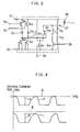
- a laser driver such as shown in Fig. 3.
- the same components are designated by the same reference numerals as in Fig. 1, and therefore the detailed description thereof is omitted.
- an offset current supplying FET Q49 and voltage dividing FET Q50 are connected between the power supply terminal 32 and output terminal 37. Namely, the source electrode of FET Q49 is connected to the power supply terminal 32, the drain electrode of FET Q49 is connected to the source terminal of FET Q50, and the drain electrode of FET Q50 is connected to the output terminal 37. Further, the gate electrode of FET Q49 is connected to the offset current control terminal 36.
- a pair of voltage dividing resisters R41 and R42 are series connected between the earth terminal 31 and power supply terminal 32, and the junction point therebetween is connected to the gate electrode of FET Q50.
- the FETs Q49 and Q50 are formed to have the same structure and parameters such as pattern dimensions of parts and threshold voltage. Further, the voltage dividing resistors R41 and R42 are formed to have the same resistance. For this reason, a potential at the gate electrode of FET Q50 is set to -2.6V which is a half of the power supply voltage -5.2V applied between the earth terminal 31 and power supply terminal 32. In addition, the resistance of the resistors R41 and R42 is set to about 1k ⁇ , respectively, so as to avoid the increase of current consumption. In this case, the total power consumption of about 13.5mW is consumed by the resistors R41 and R42, and such value can be negligible in actual use.
- the FETs Q49 and Q50 have the identical structure and the gate potential of FET Q50 is fixed to -2.6V. For this reason, when both of the offset current I o and switching current I s becomes zero, a voltage V DS between the drain and source electrodes of FET Q49 is held 2.6V+V th , and another voltage V DS between the drain and source electrodes of FET Q50 is held 2.6V-V th where V th (V) is a threshold voltage of FET Q49. Further, a voltage V GD between the gate and drain electrodes of FET Q50 is held -2.6V and another V GD between the gate and drain electrodes of FET Q49 is held about 2V th -2.6V.
- V GD of FET Q49 is held in the range from -4.6V to -3.5V when the value of V th is set to the range between -1V and -0.5V. Accordingly, Fig. 3, since a load voltage exceeding the reverse withstanding voltage from -6V to -5V between the gate and drain electrodes cannot be applied to the respective FETs Q49 and Q50, a laser driver having high reliability can be obtained.
- the additional function to vary the offset current I o within the range from 0mA to 100mA is needed in accordance with the threshold current value of laser diode 38 to be driven as described above.
- the additional function is needed to vary the offset voltage of output signal.
- the variable range from about O to 100mA is needed for the offset current I o in the laser driver.
- the respective gate electrode of FETs Q49 and Q50 must have the gate width of about 400»m through 600»m in order to flow a relatively large current through the FETs Q49 and Q50.
- the respective voltage V GS between the gate and source electrodes of FETs Q49 and Q50 is set to 0.4V through 0.5V.
- a parasitic capacitor C gd between the gate and drain electrodes of FET Q50 has a capacitance more or less exceeding 0.3pF through 0.5pF due to the great width of gate electrode and the forward biasing of 0.4V through 0.5V between the gate and source electrodes. Further, by the combination of capacitance of capacitor C gd of FET Q50 and resistances of voltage dividing resistors R41 and R42, the transition characteristic of output current outputted from the output terminal should have long time-dependant component.
- a time constant defined as the product of the parallel composite resistance of resistors R41 and R42 and the capacitance of capacitor C gd is caluculated to 150psec through 250psec.
- Such order of time constant cannot be neglected in ultra high speed modulation characteristic on the order of Gb/sec. Such situation will be explained with reference to Fig. 4.
- the respective voltage V GS of FETs Q49 and Q50 is reverse biased as V GS ⁇ V th so that the above described deterioration of high frequency modulating signal waveform due to the capacitor C gd is not remarkable.
- the DC level of offset current I o is indicated by g when the respective FETs Q49 and Q50 are forward biased at 0.4V through 0.5V between the gate and source electrodes thereof.
- the level of offset current I o is set to a great value of 80mA through 100mA, and the amplitude of switching current I s is indicated by h and the output waveform of switching current I s is indicated by i .
- the peak level of output current waveform i cannot reach the level of offset current I o indicated by g . Accordingly, the high level of envelope of output current waveform is different from the DC level of offset current I o .
- the above-mentioned time constant could be reduced as desired.
- the resistances of resistors R41 and R42 were set to 100 ⁇ , respectively, the above-mentioned time constant could be 15psec through 25psec and the problem of waveform deterioration could be avoided.
- the total electric power consumed in the resistors R41 and R42 could reach 140mW through 150Mw to cause practical problem.
- an object of the present invention is to, therefore, provide a semiconductor integrated circuit device in which wasted power is not consumed, and the deterioration of FETs due to the application of voltage close to the reverse withstanding voltage thereof between the gate and drain electrodes thereof and deterioration of high frequency modulating signal waveform can be eliminated.
- a semiconductor integrated circuit device for applying to an external load connectable between an output terminal and a first power supply terminal, a switching signal and an offset signal in superposed relation to each other, the device comprising supplying means for supplying an offset signal to said output terminal, and characterised by said supplying means comprising a first field effect transistor having a drain electrode connected to said output terminal, and a second field effect transistor having the substantially same characteristics as said first field effect transistor, said second field effect transistor having a drain electrode connected to a source electrode of said first field effect transistor, a gate electrode connected to a control terminal receptive of a control signal effective to control said offset signal, and a source electrode connected to a second power supply terminal; and constant-voltage generating means for generating and applying a constant voltage to a gate electrode of said first field effect transistor, said constant-voltage generating means comprising a resistor connected between said first power supply terminal and said gate electrode of the first field effect transistor, and a plurality of diodes having the substantially same characteristics and being forwardly series
- the series-connected resistor and the plurality of diodes actually function as a constant voltage generating circuit. Namely, since the anode of first stage diode in the plural diodes is held at the potential which is half of the voltage applied between the power supply terminals, the gate electrode of first FET is always held at half of the power supply voltage. For this reason, when the power supply voltage is set to, for example, -5.2V, and the threshold voltage of first FET (or second FET) is set to V th , the voltages V DS between the drain and source electrodes of first and second FETs are held at 2.6v+V th and 2.6V-V th , respectively.
- the voltages V GS between the gate and drain electrodes of first and second FETs are held at about -2.6V and 2V th -2.6V, respectively. Normaldy, since the value of V th is selected between about -1V and -0.5V, the voltage V GD of second FET is held at about -4.6V through -3.5V.
- each of the plural diodes has an internal resistance much smaller than that of the resister in the above-described constant voltage generating circuit, the value of current flowing through this circuit is supressed small substantially according to the resistance of resistor, and therefore the power consumption is sufficiently reduced in the constant voltage generating circuit.
- the parallel composite resistance of the resistor and the plural diodes is substantially equal to combined internal resistance of the plurality of series-connected diodes, the time constant defined by the product of parastic capacity between the gate and drain region of first FET and the parallel composite resistance is sufficiently reduced. For this reason, the deterioration of high frequency modulating signal waveform can be sufficiently supressed.
- Fig. 1 is an equivalent circuit diagram of the prior art laser driver
- Fig. 2 is a waveform diagram showing the output current waveform of the prior art laser driver shown in Fig. 1 and the relation between offset and switching currents
- Fig. 3 is an equivalent circuit diagram of the laser driver prior-devised by the inventor
- Fig. 4 is a waveform diagram showing the relation among the offset current, the amplitude of switching current and the waveform of output current in the prior-devised structure shown in Fig. 3
- Fig. 5 is an equivalent circuit diagram of a first embodiment of the laser driver according to the present invention
- Fig. 6 is an equivalent circuit diagram of a second embodiment of the laser driver according to the present invention.
- Various types of field effect transistors used in the embodiment is composed of Schottky junction type field effect transistor and various types of diodes used in the embodiment is composed of Schottky junction type diodes. Further, these field effect transistors and diodes are formed on a semiconductor substrate composed of GaAs together with other components.
- the semiconductor laser driver is provided with an earth or positive power terminal 1 and a negative power supply terminal 2. Normally, a voltage of -5.2V is applied between the earth terminal 1 and power supply terminal 2 to power the semiconductor laser driver. Further, a pair of first and second level-shifting circuits 25 and 26 are connected in parallel to each other between the earth terminal 1 and power supply terminal 2.
- the first level-shifting circuit 25 is comprised of a field effect transistor (hereinafter, referred to as "FET") Q11, level-shifting diode D11 and current-supplying FET Q13 connected in series to each other.
- FET field effect transistor
- a gate electrode of the FET Q11 is connected to an input terminal 3 and receives an input signal such that the first level-shifting circuit 25 shifts or regulates the voltage level of input signal according to a given standard.
- the second level-shifting circuit 26 is comprised of a FET Q12, level-shifting diode D12 and current-supplying FET Q14 connected in series to each other.
- a gate electrode of the FET Q12 is connected to a reference terminal 4 and receives a reference signal such as, for example, a signal having a phase opposite to that of the input signal so that the second level-shifting circuit 26 shifts or regulates the voltage level of reference signal according to the given standard.
- An output differentially-operating circuit 27 is connected subsequently to the first and second level-shifting circuits 25 and 26 to differentially operate or process the level-shifted input and reference signals with each other to thereby produce an output signal in the form of a switching current I s effective to drive an external laser diode 8.
- the differentially-operating circuit 27 is comprised of a pair of FETs Q15 and Q16 connected in parallel to each other and a current supplying FET Q17 connected in series to the pair of FETs Q15 and Q16. More specifically, a gate electrode of the FET Q15 is branch-connected to a cathode of the level-shifting diode D12 and a drain electrode of the FET Q15 is connected to the earth terminal 1.
- a gate electrode of the FET Q16 is branch-connected to a cathode of the level-shifting diode D11 and a drain electrode of the FET Q16 is connected to an output terminal 7 which is connectable to the external laser diode 8.
- the current supplying FET Q17 has a source electrode connected to the power supply terminal 2, a drain electrode connected to the source electrodes of FETs Q15 and Q16, and a gate electrode connected to a switching current control terminal 5 receptive of a first control signal effective to control or regulate the switching current I s .
- An offset current supplying circuit is connected subsequently to the differentially-operating circuit 27 to supply an offset or bias current I o to the external laser diode 8 in superposed relation to the switching current I s .
- the offset current supplying circuit is comprised of an offset current supplying FET Q18 for supplying the offset current I o and a voltage-dividing FET Q19 connected in series to the FET Q18 for dividing a voltage between the power supply terminal 2 and the output terminal 7.
- the offset current supplying FET Q18 has a source electrode connected to the power supply terminal 2, a drain electrode connected to a source electrode of the FET Q19 and a gate electrode connected to an offset current control terminal 6 receptive of a second control signal effective to control or regulate the offset current I o .
- the voltage-dividing FET Q19 has a drain electrode connected to the output terminal 7.
- the FETs Q18 and Q19 have electrically and thermally identical characteristics. Stated otherwise, the FETs Q18 and Q19 have substantially the same structure and parameter with respect to, for example, the pattern dimension of portions thereof and threshold voltage.
- a constant voltage generating circuit 28 is connected subsequently to the series-connected FETs Q18 and Q19.
- the constant voltage generating circuit 28 is comprised of a resistor R11 and group of diodes D13-D16 series-connected to each other between the earth terminal 1 and power supply terminal 2.
- the constant voltage generating circuit 28 is connected at its junction between the resistor R11 and anode of the diode D13 to a gate electrode of the FET Q19 to apply thereto a constant voltage so as to control the voltage-dividing FET Q19.
- the resistor R11 has a resistance of 1k ⁇
- each of the diodes D13-D16 has an internal resistance r i of less than 10 ⁇ and a forward drop voltage V f of 0.65V between the cathode and anode thereof.
- the external laser diode 8 is connected between the earth terminal and the output terminal 7 as a load.
- An input signal is inputted from the input terminal 3 into the gate electrode of FET Q16 included in the differentially-operating circuit 27 through the first level-shifting circuit 25.
- a reference signal in the form of a reference voltage of -1.3V or a signal having a phase opposite to that of the input signal is inputted from the reference terminal 4 into the gate electrode of FET Q15 included in the differentially-operating circuit 27 through the second level-shifting circuit 26.
- the output differentially-operating circuit 27 operates when receiving the input and reference signals to effect intermittent switching or modulation of a drain current flowing through the current supplying FET Q17 at ultra high speed in response to the voltage difference between the input and reference signals to thereby produce a switching current I s .
- the switching current I s can be controlled or regulated according to the application of a first external control voltage to the switching current control terminal 5.
- Another drain current flowing through the FET Q19 and supplied from the FET Q18 is applied as an offset or bias current I o to the laser diode 8 in superposed relation to the switching current I s to thereby intermittently drive the laser diode 8.
- the offset current I o can be controlled or regulated according to the application of a second external control voltage to the offset current control terminal 6.
- the gate potential at the gate electrode of FET Q19 is always set to the value of -2.6V. Accordingly, the operation of FETs Q18 and Q19 is substantially identical to those used in the second prior work (art) shown in Fig. 4. Namely, when both of the offset current I o and output switching current I s are zero, a drain-source voltage V DS between the drain and source electrodes of FET Q19 equals to 2.6+V th (V), and another drain-source voltage V DS between the drain and source electrodes of FET Q18 equals to 2.6-V th (V) where V th is the threshold voltage of FET Q19.
- a gate-drain voltage V GD between the gate and drain electrodes of FET Q19 equals to -2.6V
- another gate-drain voltage V GD between the gate and drain electrodes of FET Q18 equals to 2V th -2.6V.
- V th ranges from -1V to -0.5V
- the value of V GD of FET Q18 is set to range from -4.6V to -3.5V. Consequently, in this embodiment, no excessive load voltage is applied between the gate and drain electrodes of FETS Q18 and Q19, respectively, not exceeding reverse-withstanding voltage of -6V to -5V thereof, thereby avoiding the deterioration thereof due to application of excessive load voltage thereto.
- each of the diodes D13-D16 has an internal resistance r i of less than 10 ⁇
- the time constant defined by the product of the parallel composite resistance of resistor R11 and group of diodes D13-D16, and the parastic capacity C gd (0.3pF to 0.5pF) formed between the gate and drain electrodes of FET Q19 equals to the order of C gd x40 ⁇ , i.e., 12psec to 15psec which is smaller by one order than that in the second prior work (art) structure. If the time constant has such value, the wave form of high frequency switching or modulated signal cannot be deteriorated even if the switching or modulation speed exceeds 1Gb/sec, thereby achieving an excellent ultra high frequency modulation characteristic.
- an additional resistor R12 is connected between the source electrode of offset current supplying FET Q18 and the power supply terminal 2 for monitoring the offset current I o .
- the resistance of resistor R12 is set to about 10 ⁇ .
- An offset current monitoring terminal 9 is branch-connected to the source electrode of FET Q18.
- the additional resistor R12 does not deteriorate the waveform of switching or high-frequency-modulating signal effective to intermittently switching the laser diode.
- the potential difference between the monitoring terminal 9 and the power supply terminal 2 is measured so as to easily monitor the offset current I o .
- Such monitoring is considerably effective for automatic stabilization of output of the laser diode 8, and prevention of the laser diode destruction.
- the first and second embodiments are used as a current modulating element for driving the laser diode; however, the present invention is not limited to such application. Namely, the present invention can be widely applied to a general semiconductor integrated circuit device having controlling function for offset current or voltage.
- the present invention has following advantages:
Landscapes
- Physics & Mathematics (AREA)
- Condensed Matter Physics & Semiconductors (AREA)
- General Physics & Mathematics (AREA)
- Electromagnetism (AREA)
- Optics & Photonics (AREA)
- Semiconductor Lasers (AREA)
- Control Of Electrical Variables (AREA)
- Junction Field-Effect Transistors (AREA)
- Control Of Direct Current Motors (AREA)
Applications Claiming Priority (2)
| Application Number | Priority Date | Filing Date | Title |
|---|---|---|---|
| JP63065347A JPH01237807A (ja) | 1988-03-18 | 1988-03-18 | 半導体集積回路装置 |
| JP65347/88 | 1988-03-18 |
Publications (3)
| Publication Number | Publication Date |
|---|---|
| EP0333494A2 EP0333494A2 (en) | 1989-09-20 |
| EP0333494A3 EP0333494A3 (en) | 1991-07-03 |
| EP0333494B1 true EP0333494B1 (en) | 1995-08-02 |
Family
ID=13284327
Family Applications (1)
| Application Number | Title | Priority Date | Filing Date |
|---|---|---|---|
| EP89302641A Expired - Lifetime EP0333494B1 (en) | 1988-03-18 | 1989-03-17 | Semiconductor driver for producing switching and offset signals |
Country Status (4)
| Country | Link |
|---|---|
| US (1) | US5015873A (ja) |
| EP (1) | EP0333494B1 (ja) |
| JP (1) | JPH01237807A (ja) |
| DE (1) | DE68923636T2 (ja) |
Families Citing this family (13)
| Publication number | Priority date | Publication date | Assignee | Title |
|---|---|---|---|---|
| WO1991000621A1 (en) * | 1989-06-24 | 1991-01-10 | Mitsubishi Rayon Co., Ltd. | Light-emitting diode drive circuit |
| US5319260A (en) * | 1991-07-23 | 1994-06-07 | Standard Microsystems Corporation | Apparatus and method to prevent the disturbance of a quiescent output buffer caused by ground bounce or by power bounce induced by neighboring active output buffers |
| KR950002084B1 (ko) * | 1992-12-16 | 1995-03-10 | 현대전자산업주식회사 | 고전압 노이즈 감소용 데이타 출력 버퍼회로 |
| DE4318857C1 (de) * | 1993-06-07 | 1994-07-28 | Ant Nachrichtentech | Treiberstufe für ein optisches Sendeelement |
| DE19534937C1 (de) * | 1995-09-20 | 1996-12-05 | Siemens Ag | Wellenlängenabstimmbare Laservorrichtung |
| JP3368738B2 (ja) * | 1996-01-17 | 2003-01-20 | 三菱電機株式会社 | 光送信器 |
| US5767704A (en) * | 1996-08-30 | 1998-06-16 | Larson; Francis Willard | High frequency analog switch for use with a laser diode |
| GB9619205D0 (en) * | 1996-09-13 | 1996-10-23 | Medical Research The | Controlled release repellent |
| JP4810904B2 (ja) * | 2005-07-20 | 2011-11-09 | ソニー株式会社 | 高周波スイッチ回路を有する高周波装置 |
| US8477815B2 (en) | 2011-09-07 | 2013-07-02 | Texas Instruments Incorporated | Laser driver |
| EP3531516B1 (en) * | 2016-10-20 | 2021-08-18 | Nippon Telegraph And Telephone Corporation | Directly modulated laser drive circuit |
| US10761041B2 (en) * | 2017-11-21 | 2020-09-01 | Watlow Electric Manufacturing Company | Multi-parallel sensor array system |
| CN114567151B (zh) * | 2022-02-25 | 2023-09-29 | 中国电子科技集团公司第二十九研究所 | GaAs工艺驱动电路的改善方法、电路、开关、芯片 |
Family Cites Families (7)
| Publication number | Priority date | Publication date | Assignee | Title |
|---|---|---|---|---|
| US4539686A (en) * | 1982-10-15 | 1985-09-03 | At&T Bell Laboratories | Laser driving means |
| US4634893A (en) * | 1983-01-10 | 1987-01-06 | Ncr Corporation | FET driver circuit with mask programmable transition rates |
| JPS60113546A (ja) * | 1983-11-24 | 1985-06-20 | Nec Corp | 光送信器 |
| FR2559323B1 (fr) * | 1984-02-08 | 1986-06-20 | Labo Electronique Physique | Circuit logique elementaire realise a l'aide de transistors a effet de champ en arseniure de gallium et compatible avec la technologie ecl 100 k |
| JPS62221217A (ja) * | 1986-03-24 | 1987-09-29 | Matsushita Electronics Corp | 半導体集積回路装置 |
| US4807239A (en) * | 1986-04-03 | 1989-02-21 | Copal Electronics Co., Ltd. | Drive and control circuit for laser diode |
| US4792706A (en) * | 1986-12-16 | 1988-12-20 | Texas Instruments Incorporated | ECL gates using diode-clamped loads and Schottky clamped reference bias |
-
1988
- 1988-03-18 JP JP63065347A patent/JPH01237807A/ja active Pending
-
1989
- 1989-03-15 US US07/324,219 patent/US5015873A/en not_active Expired - Lifetime
- 1989-03-17 EP EP89302641A patent/EP0333494B1/en not_active Expired - Lifetime
- 1989-03-17 DE DE68923636T patent/DE68923636T2/de not_active Expired - Fee Related
Also Published As
| Publication number | Publication date |
|---|---|
| DE68923636T2 (de) | 1996-01-11 |
| US5015873A (en) | 1991-05-14 |
| JPH01237807A (ja) | 1989-09-22 |
| DE68923636D1 (de) | 1995-09-07 |
| EP0333494A2 (en) | 1989-09-20 |
| EP0333494A3 (en) | 1991-07-03 |
Similar Documents
| Publication | Publication Date | Title |
|---|---|---|
| EP0333494B1 (en) | Semiconductor driver for producing switching and offset signals | |
| US4243951A (en) | High repetition rate driver circuit for modulation of injection lasers | |
| US6618406B1 (en) | Optical semiconductor diode driver circuit and optical tranceiver module | |
| US5546218A (en) | Drive circuit of a simiconductor optical modulator | |
| US4799224A (en) | Driver for a semiconductor laser | |
| JPH0228386A (ja) | 半導体集積回路 | |
| US6483345B1 (en) | High speed level shift circuit for low voltage output | |
| KR100649467B1 (ko) | 레이저 다이오드의 구동 회로 | |
| US6989701B2 (en) | Pulse width modulation driving apparatus for light emitting diode | |
| EP0577896A1 (en) | Preamplifier | |
| GB2024550A (en) | Integrated driver circuits | |
| US4647792A (en) | High speed laser driver | |
| US6765942B2 (en) | Optoelectronic circuit and control circuit | |
| JPH11126935A (ja) | レーザーダイオード駆動回路 | |
| US20030006842A1 (en) | Split cascode driver | |
| US4423357A (en) | Switchable precision current source | |
| JP2773484B2 (ja) | レーザダイオード駆動回路 | |
| JP3644003B2 (ja) | 光デバイスの駆動回路 | |
| JPH0254977A (ja) | 半導体レーザ駆動回路 | |
| JPS63152182A (ja) | 半導体装置 | |
| JP2973526B2 (ja) | 電界効果トランジスタ論理回路 | |
| JPH01245613A (ja) | 集積回路 | |
| JPH03235389A (ja) | レーザダイオード駆動回路 | |
| JP2606421B2 (ja) | 半導体集積回路装置 | |
| JPS63313891A (ja) | レ−ザ−ダイオ−ド駆動用半導体集積回路装置 |
Legal Events
| Date | Code | Title | Description |
|---|---|---|---|
| PUAI | Public reference made under article 153(3) epc to a published international application that has entered the european phase |
Free format text: ORIGINAL CODE: 0009012 |
|
| 17P | Request for examination filed |
Effective date: 19890325 |
|
| AK | Designated contracting states |
Kind code of ref document: A2 Designated state(s): DE FR GB |
|
| PUAL | Search report despatched |
Free format text: ORIGINAL CODE: 0009013 |
|
| AK | Designated contracting states |
Kind code of ref document: A3 Designated state(s): DE FR GB |
|
| RHK1 | Main classification (correction) |
Ipc: H03K 17/04 |
|
| 17Q | First examination report despatched |
Effective date: 19940114 |
|
| GRAA | (expected) grant |
Free format text: ORIGINAL CODE: 0009210 |
|
| AK | Designated contracting states |
Kind code of ref document: B1 Designated state(s): DE FR GB |
|
| REF | Corresponds to: |
Ref document number: 68923636 Country of ref document: DE Date of ref document: 19950907 |
|
| ET | Fr: translation filed | ||
| PLBE | No opposition filed within time limit |
Free format text: ORIGINAL CODE: 0009261 |
|
| STAA | Information on the status of an ep patent application or granted ep patent |
Free format text: STATUS: NO OPPOSITION FILED WITHIN TIME LIMIT |
|
| 26N | No opposition filed | ||
| REG | Reference to a national code |
Ref country code: GB Ref legal event code: IF02 |
|
| REG | Reference to a national code |
Ref country code: GB Ref legal event code: 732E |
|
| REG | Reference to a national code |
Ref country code: FR Ref legal event code: TP |
|
| REG | Reference to a national code |
Ref country code: GB Ref legal event code: 732E |
|
| REG | Reference to a national code |
Ref country code: FR Ref legal event code: TP |
|
| PGFP | Annual fee paid to national office [announced via postgrant information from national office to epo] |
Ref country code: GB Payment date: 20070314 Year of fee payment: 19 |
|
| PGFP | Annual fee paid to national office [announced via postgrant information from national office to epo] |
Ref country code: DE Payment date: 20070315 Year of fee payment: 19 |
|
| PGFP | Annual fee paid to national office [announced via postgrant information from national office to epo] |
Ref country code: FR Payment date: 20070308 Year of fee payment: 19 |
|
| GBPC | Gb: european patent ceased through non-payment of renewal fee |
Effective date: 20080317 |
|
| REG | Reference to a national code |
Ref country code: FR Ref legal event code: ST Effective date: 20081125 |
|
| PG25 | Lapsed in a contracting state [announced via postgrant information from national office to epo] |
Ref country code: DE Free format text: LAPSE BECAUSE OF NON-PAYMENT OF DUE FEES Effective date: 20081001 |
|
| PG25 | Lapsed in a contracting state [announced via postgrant information from national office to epo] |
Ref country code: FR Free format text: LAPSE BECAUSE OF NON-PAYMENT OF DUE FEES Effective date: 20080331 |
|
| PG25 | Lapsed in a contracting state [announced via postgrant information from national office to epo] |
Ref country code: GB Free format text: LAPSE BECAUSE OF NON-PAYMENT OF DUE FEES Effective date: 20080317 |