EP0332467A2 - Circuit pour détecter l'asservissement d'une boucle d'asservissement de phase - Google Patents
Circuit pour détecter l'asservissement d'une boucle d'asservissement de phase Download PDFInfo
- Publication number
- EP0332467A2 EP0332467A2 EP89302409A EP89302409A EP0332467A2 EP 0332467 A2 EP0332467 A2 EP 0332467A2 EP 89302409 A EP89302409 A EP 89302409A EP 89302409 A EP89302409 A EP 89302409A EP 0332467 A2 EP0332467 A2 EP 0332467A2
- Authority
- EP
- European Patent Office
- Prior art keywords
- output
- signal
- phase
- counter
- input
- Prior art date
- Legal status (The legal status is an assumption and is not a legal conclusion. Google has not performed a legal analysis and makes no representation as to the accuracy of the status listed.)
- Withdrawn
Links
Images

Classifications
-
- H—ELECTRICITY
- H03—ELECTRONIC CIRCUITRY
- H03L—AUTOMATIC CONTROL, STARTING, SYNCHRONISATION OR STABILISATION OF GENERATORS OF ELECTRONIC OSCILLATIONS OR PULSES
- H03L7/00—Automatic control of frequency or phase; Synchronisation
- H03L7/06—Automatic control of frequency or phase; Synchronisation using a reference signal applied to a frequency- or phase-locked loop
- H03L7/08—Details of the phase-locked loop
- H03L7/085—Details of the phase-locked loop concerning mainly the frequency- or phase-detection arrangement including the filtering or amplification of its output signal
- H03L7/095—Details of the phase-locked loop concerning mainly the frequency- or phase-detection arrangement including the filtering or amplification of its output signal using a lock detector
-
- Y—GENERAL TAGGING OF NEW TECHNOLOGICAL DEVELOPMENTS; GENERAL TAGGING OF CROSS-SECTIONAL TECHNOLOGIES SPANNING OVER SEVERAL SECTIONS OF THE IPC; TECHNICAL SUBJECTS COVERED BY FORMER USPC CROSS-REFERENCE ART COLLECTIONS [XRACs] AND DIGESTS
- Y10—TECHNICAL SUBJECTS COVERED BY FORMER USPC
- Y10S—TECHNICAL SUBJECTS COVERED BY FORMER USPC CROSS-REFERENCE ART COLLECTIONS [XRACs] AND DIGESTS
- Y10S331/00—Oscillators
- Y10S331/02—Phase locked loop having lock indicating or detecting means
Definitions
- the present invention relates to a phase locked loop, and more specifically to a circuit for detecting a lock of the phase locked loop.
- one typical phase locked loop has included a phase comparator receiving an input signal and a reference signal for generating a pair of phase difference signals which assume a high logic level, respectively, when a phase coincidence is achieved.
- a phase locked condition of the phase locked loop it is necessary to detect the phase coincidence between the two input signals, namely, the phase locked condition of the phase locked loop.
- the pair of phase difference signals are inputted to a logic gate circuit such as an AND gate (or a NAND gate), so that a high level signal (a low level signal) is generated when the phase locked loop is in a locked condition.
- a lock condition of the phase locked loop is detected.
- phase lock signal is generated.
- the phase locked loop becomes out of phase from a phase locked (or in-phase) condition and therefore operates towards an in-phase condition again, the phase of a signal to be synchronized is caused to alternately and repeatedly advance and delay with respect to the phase of a synchronizing signal, but the phase difference gradually decreases, so that, the phase of the signal to be synchronized is finally rendered consistent wih the phase of the synchronizing signal.
- phase locked loop has an inherent oscillation frequency. Accordingly, in the course of the transient response of the phase locked loop, namely, in the process in which the signal to be synchronized is being brought into phase with the synchronizing signal, an erroneous lock signal is generated at each moment the two signals become instantaneously in phase.
- Another object of the present invention is to provide a phase lock detection circuit which will not generate an erroneous lock signal in the transient process of the phase locked loop toward to the phase locked condition.
- a further object of the present invention is to provide a phase lock detection circuit which can generate a phase lock signal only when a phase coincidence condition continues at least for a predetermined period of time which will allow to conclude that a stable locked condition has be realized.
- a circuit for detecting a lock of a phase locked loop comprising phase comparison means receiving a first signal and a second signal for generating a phase difference signal, waveform shaping means connected to receive the phase difference signal for generating an output signal when the phase difference signal indicates a phase difference exceeding a predetermined value, a multi-stage counter having a frequency division function and having a reset input connected to receive the output signal of the waveform shaping means, input control means connected to receive the first signal and an output of the multi-stage counter and having an output connected to an input of the multi-stage counter for allowing the first signal to be applied to the multi-stage counter only when the output of the multi-stage counter is at a predetermined logic level.
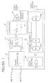
- phase lock detection circuit includes a phase comparator 10 receiving a reference input signal "a” and a signal “b” to be synchronized and outputting a pair of phase difference signals "c" and "d” which are supplied to a two-input logic circuit 12 such as a AND gate.
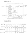
- the phase comparator 10 can be of the sequential logic circuit type and shown in Figure 2.
- the shown sequential logic circuit type of phase comparator is composed of some number of NAND gates connected as shown.
- Figure 3 is a timing chart illustrating the relation between the inputs "a” and “b” and the outputs "c” and “d” of the phase comparator shown in Figure 2.
- the outputs "c" and"d" of the phase comparator shown in Figure 2 are supplied to a low pass filter (not shown) through a charge pump (not shown), so that a digital signal is converted into an analog signal, which is applied, namely, fed back to a voltage controlled oscillator (not shown). An output of the voltage controlled oscillator is fed back to the reference input of the phase comparator, and is outputted as a synchronizing signal.
- the phase locked loop is constituted, but, since the fundamental construction of the phase locked loop itself is well known to persons skilled in the art, a further explanation and a drawing indicating an example of the phase locked loop will be omitted.
- an output "e” of the logic gate 12 is inputted to an integrater 14 composed of a resister R and a capacitor C, which are connected in a well known manner to form a basic simple analog integrater.
- An output of the integrater 14 is connected to an input of a schmitt circuit 16, whose output "f” is connected to a reset terminal of an N-stage counter 18.
- the counter 18 is composed of, for example, a plurality of flipflops 18A-18N cascaded in a well known manner to form a binary counter.
- N is not less than 2.
- An input of a first stage 18A of the N-stage counter 18 is connected to an output "g" of an input control circuit 20, which can be formed of an AND gate and which has a data input connected to receive the reference signal "a' and a control input connected to an output "h” of a final state 18N of the N-stage counter 18.
- the output "h” of the final stage 18N of the N-stage counter 18 forms a lock output of the lock detection circuit.
- phase lock detection circuit Assume that the relation between the inputs "a” and “b” changes from a phase locked (in-phase) condition to an out-of-phase condition. As a result of the out-of-phase, the logic gate (AND gate) 12 will output a low level signal "e", which is fed through the integrater 14 and the schmitt circuit 16 to the N-stage counter 18 as a reset signal "f". When the reset signal "f' is at a low level, the N-stage counter 18 is maintained in a reset condition, so that the lock output "h" of a high level is generated.
- the N-stage counter 18 will output a high level of lock output "h" representative of an unlock condition. Accordingly, if the two inputs "a" and “b" of the phase comparator are in an out-of-phase condition, since there is maintained a condition in which the N-stage counter 18 is reset by the reset signal "f", the lock signal "h" continues to indicate the unlock condition.
- the logic gate 12 will bring its output “e” into a high level.
- This change of the logic gate output “e” is transmitted to the reset input "f" of the N-stage counter through the integrater 14 and the schmitt circuit 16, that the reset condition of the counter 18 is released.
- the lock output “h” of the counter 18 is still maintained at the high level indicative of the unlocked condition.
- the input control circuit 20 outputs the reference signal "a” as the output "g". Therefore, the N-stage counter 18 will start to count the reference signal "a” which is fed through the input control circuit 20.
- the N-stage counter 18 will continue to maintain the output signal "h” indicative of the unlocked locked condition until the counter 18 will have been supplied with the reference signal pulses of the number corresponding to 2 N-1 where "N" is the stage number of the counter 18.
- phase lock detection circuit if the two inputs "a” and “b” become out of phase after the moment the two inputs “a” and “b” become in phase and before 2 N-1 pulses of the reference signal “a” are generated, the counter 18 will then reset by the reset signal "f” before the counter 18 generates the low level output signal "h” indicative of the locked condition. Accordingly, the low level output signal "h” indicative of the locked condition is generated only in the case that the two inputs "a” and “b” are maintained in phase for a period in which the 2 N-1 pulses of the reference signal "a” are generated.
- the phase comparator will continue to operate for the purpose of detecting a possible minute phase difference between the reference signal "a" and the signal "b" to be synchronized with the reference signal, so that a detected phase difference is fed back to the voltage controlled oscillator (not shown) through the loop filter (not shown) so that the locked condition is maintained.
- the logic gate 12 generates a very narrow or thin pulse at the timing of the reference signal "a” even in the locked condition.
- the integrater 14 and the schmitt circuit 16 are provided to neglect a minute phase difference.
- the input control circuit 20 operates to prevent the reference signal "a” from being inputted to the counter 18 when the circuit is in a stable locked condition and on the other hand to supply the reference signal "a” to the counter 18 only when the circuit is not in a stable locked condition and for a period from the moment the two inputs "a” and “b” become in phase to the moment the 2 N-1 pulses of the reference signal "a” have been generated.
- the counter 18 is maintained in a reset condition, the counter will not perform a frequency division operation.
- the input control circuit 20 can be formed of not only an AND gate but also a NAND gate.
- the logic gate 12 is formed of the AND gate but can be formed of a NAND gate.
- the N-stage counter 18 may be an up-counter, and the stage number "N" of the counter 18 is determined by considering the inherent oscillation frequency depending upon the loop gain and the dumping property of the phase lock loop. If the reference signal "a" has a frequency fr, it is possible to discriminate a time expressed by 1 / fr ⁇ 2 N-1 .
- the schmitt circuit 16 In the case of the time constant A, in response to a low level of the output signal "e", the output of the integrater 14 will fall down less than a threshold V T of the schmitt circuit 16, and therefore, the schmitt circuit 16 will change the level of the output reset signal "f". On the other hand, in the case of the time constant B, the output of the integrater 14 will not fall down less than the threshold V T of the schmitt circuit 16, and therefore, the schmitt circuit 16 will not change the level of the output reset signal "f".
- the acceptable phase difference can be determined by the RC time constant.
- the phase lock detection circuit in accordance with the present invention can conclude that the phase lock has been realized, only when a stable phase locked condition is achieved. In other words, the phase lock detection circuit in accordance with the present invention will never generate an erroneous lock detection signal in the transient process of the phase locked loop towards to the stable phase locked condition.
Landscapes
- Stabilization Of Oscillater, Synchronisation, Frequency Synthesizers (AREA)
- Manipulation Of Pulses (AREA)
Applications Claiming Priority (2)
| Application Number | Priority Date | Filing Date | Title |
|---|---|---|---|
| JP57481/88 | 1988-03-10 | ||
| JP63057481A JPH01231430A (ja) | 1988-03-10 | 1988-03-10 | Pllロック検出回路 |
Publications (2)
| Publication Number | Publication Date |
|---|---|
| EP0332467A2 true EP0332467A2 (fr) | 1989-09-13 |
| EP0332467A3 EP0332467A3 (fr) | 1990-10-17 |
Family
ID=13056905
Family Applications (1)
| Application Number | Title | Priority Date | Filing Date |
|---|---|---|---|
| EP19890302409 Withdrawn EP0332467A3 (fr) | 1988-03-10 | 1989-03-10 | Circuit pour détecter l'asservissement d'une boucle d'asservissement de phase |
Country Status (3)
| Country | Link |
|---|---|
| US (1) | US4929916A (fr) |
| EP (1) | EP0332467A3 (fr) |
| JP (1) | JPH01231430A (fr) |
Cited By (5)
| Publication number | Priority date | Publication date | Assignee | Title |
|---|---|---|---|---|
| EP0433120A1 (fr) * | 1989-11-16 | 1991-06-19 | Fujitsu Limited | circuit synthétiseur PLL |
| US5189379A (en) * | 1989-11-16 | 1993-02-23 | Fujitsu Limited | Pulse width detecting circuit and PLL synthesizer circuit using the same |
| WO1994008285A1 (fr) * | 1992-10-02 | 1994-04-14 | Compaq Computer Corporation | Procede et appareil de mise en route d'une horloge numerique de systeme informatique |
| US5589795A (en) * | 1993-12-23 | 1996-12-31 | Nokia Mobile Phones Ltd. | Method and arrangement for controlling a loop filter |
| WO2000027033A1 (fr) * | 1998-11-04 | 2000-05-11 | Broadcom Corporation | Detecteur de verrouillage pour boucles a verrouillage de phase |
Families Citing this family (16)
| Publication number | Priority date | Publication date | Assignee | Title |
|---|---|---|---|---|
| US5164966A (en) * | 1991-03-07 | 1992-11-17 | The Grass Valley Group, Inc. | Nrz clock and data recovery system employing phase lock loop |
| US5126690A (en) * | 1991-08-08 | 1992-06-30 | International Business Machines Corporation | Phase locked loop lock detector including loss of lock and gain of lock detectors |
| US5168245A (en) * | 1991-10-30 | 1992-12-01 | International Business Machines Corporation | Monolithic digital phaselock loop circuit having an expanded pull-in range |
| US5394444A (en) * | 1993-07-12 | 1995-02-28 | Motorola, Inc. | Lock detect circuit for detecting a lock condition in a phase locked loop and method therefor |
| US5422529A (en) * | 1993-12-10 | 1995-06-06 | Rambus, Inc. | Differential charge pump circuit with high differential and low common mode impedance |
| JPH10500260A (ja) | 1994-02-15 | 1998-01-06 | ランバス・インコーポレーテッド | 位相検出誤りが最小の位相検出器 |
| AU1841895A (en) * | 1994-02-15 | 1995-08-29 | Rambus Inc. | Delay-locked loop |
| US6642746B2 (en) | 1996-01-02 | 2003-11-04 | Rambus Inc. | Phase detector with minimized phase detection error |
| US5825209A (en) * | 1997-02-27 | 1998-10-20 | Rambus Inc. | Quadrature phase detector |
| US6011412A (en) * | 1998-05-01 | 2000-01-04 | International Business Machines Corporation | Frequency shift detection circuit with selectable granularity |
| US6191613B1 (en) | 1999-07-29 | 2001-02-20 | Xilinx, Inc. | Programmable logic device with delay-locked loop |
| US6760394B1 (en) * | 1999-08-11 | 2004-07-06 | Broadcom Corporation | CMOS lock detect with double protection |
| US7323946B2 (en) * | 2005-10-20 | 2008-01-29 | Honeywell International Inc. | Lock detect circuit for a phase locked loop |
| CN1980064B (zh) * | 2005-11-29 | 2010-10-06 | 中芯国际集成电路制造(上海)有限公司 | 锁相环指示器 |
| JP2008131353A (ja) * | 2006-11-21 | 2008-06-05 | Matsushita Electric Ind Co Ltd | Pllロック検出回路および半導体装置 |
| US9503104B2 (en) * | 2014-06-11 | 2016-11-22 | Texas Instruments Incorporated | Low power loss of lock detector |
Family Cites Families (2)
| Publication number | Priority date | Publication date | Assignee | Title |
|---|---|---|---|---|
| US4122405A (en) * | 1977-10-21 | 1978-10-24 | National Semiconductor Corporation | Digital logic level signal indication of phase and frequency lock condition in a phase-locked loop |
| JPS60247330A (ja) * | 1984-05-22 | 1985-12-07 | Mitsubishi Electric Corp | アンロツク検出回路 |
-
1988
- 1988-03-10 JP JP63057481A patent/JPH01231430A/ja active Pending
-
1989
- 1989-03-10 US US07/321,685 patent/US4929916A/en not_active Expired - Lifetime
- 1989-03-10 EP EP19890302409 patent/EP0332467A3/fr not_active Withdrawn
Cited By (8)
| Publication number | Priority date | Publication date | Assignee | Title |
|---|---|---|---|---|
| EP0433120A1 (fr) * | 1989-11-16 | 1991-06-19 | Fujitsu Limited | circuit synthétiseur PLL |
| US5189379A (en) * | 1989-11-16 | 1993-02-23 | Fujitsu Limited | Pulse width detecting circuit and PLL synthesizer circuit using the same |
| WO1994008285A1 (fr) * | 1992-10-02 | 1994-04-14 | Compaq Computer Corporation | Procede et appareil de mise en route d'une horloge numerique de systeme informatique |
| US5589795A (en) * | 1993-12-23 | 1996-12-31 | Nokia Mobile Phones Ltd. | Method and arrangement for controlling a loop filter |
| WO2000027033A1 (fr) * | 1998-11-04 | 2000-05-11 | Broadcom Corporation | Detecteur de verrouillage pour boucles a verrouillage de phase |
| US6211742B1 (en) | 1998-11-04 | 2001-04-03 | Broadcom Corporation | Lock detector for phase locked loops |
| US6580328B2 (en) | 1998-11-04 | 2003-06-17 | Broadcom Corporation | Lock detector for phase locked loops |
| US6803828B2 (en) | 1998-11-04 | 2004-10-12 | Broadcom Corporation | Lock detector for phase locked loops |
Also Published As
| Publication number | Publication date |
|---|---|
| JPH01231430A (ja) | 1989-09-14 |
| EP0332467A3 (fr) | 1990-10-17 |
| US4929916A (en) | 1990-05-29 |
Similar Documents
| Publication | Publication Date | Title |
|---|---|---|
| US4929916A (en) | Circuit for detecting a lock of a phase locked loop | |
| US5164966A (en) | Nrz clock and data recovery system employing phase lock loop | |
| US5126690A (en) | Phase locked loop lock detector including loss of lock and gain of lock detectors | |
| US7187738B2 (en) | Processing high-speed digital signals | |
| EP0639004B1 (fr) | Procédé et dispositif de retard numérique de temps | |
| US4751469A (en) | Phase coincidence detector | |
| EP0252444B1 (fr) | Boucles d'asservissement de phase numériques | |
| US5909130A (en) | Digital lock detector for phase-locked loop | |
| US4287480A (en) | Phase locked loop out-of-lock detector | |
| EP0637138A1 (fr) | Circuit de détection de synchronisation | |
| US4959617A (en) | Dual state phase detector having frequency steering capability | |
| JPH04320109A (ja) | データエツジ遷移位相判別回路 | |
| US5457428A (en) | Method and apparatus for the reduction of time interval error in a phase locked loop circuit | |
| US5574757A (en) | Phase-locked loop circuit having a timing holdover function | |
| US6757349B1 (en) | PLL frequency synthesizer with lock detection circuit | |
| US4068181A (en) | Digital phase comparator | |
| US5506531A (en) | Phase locked loop circuit providing increase locking operation speed using an unlock detector | |
| KR100709518B1 (ko) | 위상 동기 루프 회로 | |
| KR100335697B1 (ko) | 주파수 편차 검출 장치 및 방법 | |
| US5734273A (en) | Phase lock detector | |
| EP1780893A1 (fr) | Circuit de réinitialisation de boucle à verrouillage de phase lors d'une perte du verrouillage | |
| US4573024A (en) | PLL having two-frequency VCO | |
| RU2119717C1 (ru) | Устройство фазовой синхронизации | |
| KR100341580B1 (ko) | 위상 고정 루프를 위한 락 디텍터 회로 | |
| GB2030745A (en) | Digital frequency quadrupler |
Legal Events
| Date | Code | Title | Description |
|---|---|---|---|
| PUAI | Public reference made under article 153(3) epc to a published international application that has entered the european phase |
Free format text: ORIGINAL CODE: 0009012 |
|
| 17P | Request for examination filed |
Effective date: 19890329 |
|
| AK | Designated contracting states |
Kind code of ref document: A2 Designated state(s): DE GB NL |
|
| PUAL | Search report despatched |
Free format text: ORIGINAL CODE: 0009013 |
|
| AK | Designated contracting states |
Kind code of ref document: A3 Designated state(s): DE GB NL |
|
| 17Q | First examination report despatched |
Effective date: 19930422 |
|
| STAA | Information on the status of an ep patent application or granted ep patent |
Free format text: STATUS: THE APPLICATION IS DEEMED TO BE WITHDRAWN |
|
| 18D | Application deemed to be withdrawn |
Effective date: 19931103 |