EP0330189A2 - Semiconductor crystal pulling method - Google Patents
Semiconductor crystal pulling method Download PDFInfo
- Publication number
- EP0330189A2 EP0330189A2 EP89103115A EP89103115A EP0330189A2 EP 0330189 A2 EP0330189 A2 EP 0330189A2 EP 89103115 A EP89103115 A EP 89103115A EP 89103115 A EP89103115 A EP 89103115A EP 0330189 A2 EP0330189 A2 EP 0330189A2
- Authority
- EP
- European Patent Office
- Prior art keywords
- crystal
- impurity
- resistivity
- material melt
- melt
- Prior art date
- Legal status (The legal status is an assumption and is not a legal conclusion. Google has not performed a legal analysis and makes no representation as to the accuracy of the status listed.)
- Granted
Links
Images


Classifications
-
- C—CHEMISTRY; METALLURGY
- C30—CRYSTAL GROWTH
- C30B—SINGLE-CRYSTAL GROWTH; UNIDIRECTIONAL SOLIDIFICATION OF EUTECTIC MATERIAL OR UNIDIRECTIONAL DEMIXING OF EUTECTOID MATERIAL; REFINING BY ZONE-MELTING OF MATERIAL; PRODUCTION OF A HOMOGENEOUS POLYCRYSTALLINE MATERIAL WITH DEFINED STRUCTURE; SINGLE CRYSTALS OR HOMOGENEOUS POLYCRYSTALLINE MATERIAL WITH DEFINED STRUCTURE; AFTER-TREATMENT OF SINGLE CRYSTALS OR A HOMOGENEOUS POLYCRYSTALLINE MATERIAL WITH DEFINED STRUCTURE; APPARATUS THEREFOR
- C30B15/00—Single-crystal growth by pulling from a melt, e.g. Czochralski method
- C30B15/02—Single-crystal growth by pulling from a melt, e.g. Czochralski method adding crystallising materials or reactants forming it in situ to the melt
- C30B15/04—Single-crystal growth by pulling from a melt, e.g. Czochralski method adding crystallising materials or reactants forming it in situ to the melt adding doping materials, e.g. for n-p-junction
-
- C—CHEMISTRY; METALLURGY
- C30—CRYSTAL GROWTH
- C30B—SINGLE-CRYSTAL GROWTH; UNIDIRECTIONAL SOLIDIFICATION OF EUTECTIC MATERIAL OR UNIDIRECTIONAL DEMIXING OF EUTECTOID MATERIAL; REFINING BY ZONE-MELTING OF MATERIAL; PRODUCTION OF A HOMOGENEOUS POLYCRYSTALLINE MATERIAL WITH DEFINED STRUCTURE; SINGLE CRYSTALS OR HOMOGENEOUS POLYCRYSTALLINE MATERIAL WITH DEFINED STRUCTURE; AFTER-TREATMENT OF SINGLE CRYSTALS OR A HOMOGENEOUS POLYCRYSTALLINE MATERIAL WITH DEFINED STRUCTURE; APPARATUS THEREFOR
- C30B15/00—Single-crystal growth by pulling from a melt, e.g. Czochralski method
- C30B15/10—Crucibles or containers for supporting the melt
- C30B15/12—Double crucible methods
-
- H—ELECTRICITY
- H10—SEMICONDUCTOR DEVICES; ELECTRIC SOLID-STATE DEVICES NOT OTHERWISE PROVIDED FOR
- H10P—GENERIC PROCESSES OR APPARATUS FOR THE MANUFACTURE OR TREATMENT OF DEVICES COVERED BY CLASS H10
- H10P14/00—Formation of materials, e.g. in the shape of layers or pillars
- H10P14/20—Formation of materials, e.g. in the shape of layers or pillars of semiconductor materials
-
- Y—GENERAL TAGGING OF NEW TECHNOLOGICAL DEVELOPMENTS; GENERAL TAGGING OF CROSS-SECTIONAL TECHNOLOGIES SPANNING OVER SEVERAL SECTIONS OF THE IPC; TECHNICAL SUBJECTS COVERED BY FORMER USPC CROSS-REFERENCE ART COLLECTIONS [XRACs] AND DIGESTS
- Y10—TECHNICAL SUBJECTS COVERED BY FORMER USPC
- Y10S—TECHNICAL SUBJECTS COVERED BY FORMER USPC CROSS-REFERENCE ART COLLECTIONS [XRACs] AND DIGESTS
- Y10S117/00—Single-crystal, oriented-crystal, and epitaxy growth processes; non-coating apparatus therefor
- Y10S117/90—Apparatus characterized by composition or treatment thereof, e.g. surface finish, surface coating
Definitions
- This invention relates to a crystal pulling method for growing semiconductor crystal using a crucible called an integral type double crucible, and more particularly to a uniform resistivity control method used in a case where two kinds of dopants or two different dopant concentration melts are used.
- impurity concentration distribution C in the longitudinal direction of the grown single crystal can be expressed as follows.
- C kCo(1-G) k-1
- k a segregation coefficient of dopant
- Co the initial impurity concentration of the melt
- G solidification ratio. Therefore, the impurity concentration distribution in the longitudinal direction significantly varies when k is small, thus lowering the yield of the single crystal having a desired preset resistivity range.
- inner crucible 2 is arranged as a floating crucible inside outer crucible 1, and small hole 3 is formed in the bottom portion of inner crucible 2.
- the balance between the buoyancy and gravitational force of the inner crucible is utilized, for example, or the outer crucible is lifted relative to the fixed inner crucible, so that melt 5 can be supplied from the outer crucible to the inner crucible, thus keeping the height h of the surface level of the melt in the inner crucible at a constant level.
- the impurity concentration of melt 5 in the outer crucible is Co
- the impurity concentration of melt 4 in the inner crucible is Co/k (k is a segregation coefficient).
- the concentration of impurity taken into pulling crystal 6 becomes Co in the pulling process in which surface level h of the melt is kept constant.
- melt pure silicon or germanium
- impurity concentration of pulling crystal 6 can also be kept at constant value Co.
- the melt is consumed.
- the melt surface level in the inner crucible cannot be kept constant, and the impurity concentration of crystal 6 will vary (increase) as the solidification ratio increases. That is, the impurity concentration can be kept constant only within the following range of the solidification ratio X: O S X -5 1-(h/H) (1) where H is the initial surface level of the melt in the outer crucible, and h is the surface level of the melt in the inner crucible to be kept constant during the pulling process.
- the resistivity can be kept constant only when the solidification ratio is less than 0.6 to 0.7. If the solidification ratio becomes larger, the resistivity will significantly vary.
- the constant resistivity of the crystal could not be obtained even in the range of the solidification ratio expressed by equation (1) when the floating type double crucible method was effected to be intended to grow crystal having constant and high resistance in its longitudinal direction.
- This problem occurs when, for example, the low donor (phosphorus P) concentration is used to grow high resistance N-type silicon single crystal with the resistivity of more than 20 0*crn and so the donor concentration is not sufficiently high with respect to the acceptor concentration of boron (B), aluminum (At) or the like flowing out of the quartz crucible.
- the actual resistivity value indicated by mark •
- the resistivity value of the crystal cannot be determined only by the concentration (indicated by mark o) of doped donor impurity (P).
- a pulling apparatus having an integral type double crucible Japanese Patent Application No. 61-221896, or US Patent Application No. 091,947 filed on September 1, 1987.
- the pulling apparatus is shown in Fig. 1.
- 11 denotes an outer crucible
- 14 denotes a cylindrical separation wall integrally and coaxially formed with outer crucible 11.
- the inner space of outer crucible 11 is divided into inner chamber 20 and outer chamber 21 by separation wall 14.
- Inner chamber 20 and outer chamber 21 are connected with each other by means of small hole 15 and narrow pipe-like coupling tube 16 formed with small hole 15.
- melt ML2 in outer chamber 21 is supplied to inner chamber 20 while single crystal 17 is being pulled from melt ML1 in the inner chamber.
- the impurity of melt ML1 in the inner chamber is inhibited from flowing into the outer chamber by the preset length L of coupling tube 16 not only during the pulling process but also when melt is not transferred from outer chamber 21 to inner chamber 20.
- Length L is determined to be larger than four times inner diameter a of tube 16.
- the integral type double crucible is different from the floating type double crucible which has only hole 15.
- One of the proposed crystal pulling methods using the integral type double crucible is to solve the problem that the impurity concentration in the longitudinal direction of crystal formed by the floating type double crucible method is limited by the solidification ratio used in equation (1).
- doped material melt ML1 impurity concentration Ci
- undoped material melt ML2 is received in outer chamber 21.
- ratio r/R of radius r of inner chamber 20 and radius R of outer chamber 21 is set to be equal to square root /k of segregation coefficient k of the doping impurity and crystal 17 of impurity concentration kCi is pulled by ⁇ R 2 ⁇ H (AH is decrease in the surface level of melt ML1) from melt ML1 in the inner chamber.
- the impurity concentration in the longitudinal direction of crystal 17 can be kept at constant value kci.
- electrically conductive impurity (B, At or the like) flows out of the crucible itself and may cause an inadvertent influence, making it difficult to attain crystal of high and constant resistivity.
- electrically conductive impurity B, At or the like
- An object of this invention is to provide a novel crystal pulling method by which substantially 100% of yield with respect to the resistivity of crystal can be attained.
- an object of this invention is to provide a crystal pulling method capable of controlling the resistivity in the longitudinal direction of crystal (1) when electrically conductive impurity of the opposite or the same conductivity type is unintentionally introduced into the melt, (2) when two kinds of electrically conductive impurity of the opposite conductivity types are intentionally introduced into the melt, or (3) when melt regions with two different impurity concentration levels of the same conductivity type are intentionally formed.
- the crystal pulling method of this invention for compensating for variation in the characteristic of the pulling crystal due to inadvertent introduction of electrically conductive impurity is effected by using an integral type double crucible.
- This crucible is divided into inner chamber 20 and outer chamber 21 by concentric or coaxial cylindrical separation wall 14.
- first doped material melt ML1 is received in inner chamber 20
- second undoped material melt ML2 is received in outer chamber 21.
- (r/R) is set to be larger than Vk so as to increase the concentration of the doping impurity in the longitudinal direction of the crystal, thus compensating for the influence by impurity of the opposite conductivity types unintentionally introduced into crystal 17.
- (r/R) is set to be smaller than Vk so as to decrease the concentration of the doping impurity in the longitudinal direction of the crystal, thus compensating for the influence by impurity of the same conductivity types unintentionally introduced into crystal 17.
- the influence of changing the resistivity in the longitudinal direction of the crystal by P-type or N-type impurity unintentionally introduced into N-type crystal can be compensated for by intentionally changing the concentration of the N-type doping impurity in the longitudinal direction of the crystal.
- the resistivity in the longitudinal direction of the pulling crystal can be controlled.
- the resistivity of more than 20 ⁇ 'cm is controlled in the longitudinal direction of phosphorus (P) doped N-type high resistance silicon single crystal pulled from a quartz crucible from which acceptor, such as B or Al, flows out of the quartz crucible, and segregation coefficient k is set at 0.35 and therefore ⁇ k is 0.59.
- the ratio of (r/R) is set to satisfy the condition of 0.85 s (r/R) > 0.59. Selection of the resistivity in the above range can be made by previously detecting the amount of acceptor flowing out of the crucible.
- ratio r/R must be understood as ratio ⁇ Si/(So+Si) when the upper surface area of melt in inner chamber 20 is Si and the upper surface area of melt in outer chamber 21 is So. That is, the above range is determined by using Si/(Si+So) instead of r/R when the crucible and separation wall are not cylindrical. The range must be set to satisfy the condition that 0.85 > ⁇ Si/(Si+So) > 0.59, for example.
- first doped material melt ML1 is received in inner chamber 20 of the integral type double crucible, and conductive impurity having a conductivity type (P) opposite to the conductivity type (N) of the doped impurity of melt ML1 is introduced into second material melt ML2 in outer chamber 21.
- the doped impurity concentration of melt ML1 which will become high during the pulling process, is reduced and compensated for by introducing melt ML2 into the inner chamber.
- the resistivity variation in the longitudinal direction of pulling crystal can thus be controlled.
- concentration C4 (x) of impurity A which has been doped into melt ML1 in the inner chamber and has been taken into pulling crystal 17 can be expressed as follows.
- k A is the segregation coefficient of impurity A
- Cm (0) is the concentration of impurity A in melt of the inner chamber at the initial pulling stage.
- concentration CB (x) of impurity B which has been doped into melt ML2 in the outer chamber and taken into pulling crystal 17 can be expressed as follows. where and k ⁇ is the segregation coefficient of impurity B and (0) is the concentration of impurity B in melt of the outer chamber at the initial pulling stage.
- the effective concentration of impurity A in the crystal with solidification ratio x can be kept at substantially the same value as that of the crystal obtained at the initial pulling stage by such a manner that one of impurity A and impurity B compensates for the other thereof.
- concentration Cm (0) of impurity B which determines (x) in equation (4) is so adjusted to substantially satisfy the following equation.
- the resistivity becomes equal in portions with solidification ratios of 0 and x (0 ⁇ x ⁇ 0.85). Further, the resistivity in portions with the segregation coefficient other than the portion of x in the solidification ratio can be controlled, so that deviation of the resistivity from a desired value can be suppressed within a relatively narrow range.
- impurity concentration Cs(x) in the pulling crystal can be expressed as follows. and k is the segregation coefficient of impurity, Ci(0) is the impurity concentration of the melt in the inner chamber at the initial pulling stage, and Co(0) is the impurity concentration of the melt in the outer chamber at the initial pulling stage.
- the impurity concentration in the crystal can be made constant in the longitudinal direction thereof.
- a coupling mechanism (15, 16) provided between the inner and outer chambers can be used to suppress the outflow of doped impurity included in melt ML1 in the inner chamber of the integral type double crucible to outer chamber 21.
- the coupling mechanism is not limited to pipe-like tube 16.
- Fig. 1 shows a crystal pulling apparatus used in one embodiment of this invention.
- graphite crucible 12 is mounted on vertically movable and rotatable crucible shaft 12, and quartz crucible 11 of 12 4) is disposed in close contact with the inner surface of graphite crucible 12.
- Quartz cylindrical separation wall 14 with radius r is coaxially disposed in and bonded to crucible 11.
- L is determined to satisfy the condition: 2 1 rr > L ⁇ 4a.
- the charge amount of silicon material was 14 kg.
- the coupling means is constructed only by means of small hole 15, supply of dopant impurity to inner chamber 20 or outer chamber 21 is effected after the grown crystal in the stage of the shouldering becomes 10 mm ⁇ and before the straight body thereof, so that reverse flow of the melt from inner chamber 20 to outer chamber 21 is prevented.
- the coupling means between the inner and outer chambers is formed of pipe-like passage 16 which has an effect of suppressing the outflow of impurity from inner chamber melt ML1 to outer chamber melt ML2, supply of dopant impurity if effected after material silicon has melted and the surface levels of the melts in the inner and outer chambers have become equal to each other.
- impurity which is flowed out from the quartz crucible is compensated for and high resistance N-type single crystal having a uniform resistivity of 50 ⁇ 'cm and 100 ⁇ 'cm, which is constant in the longitudinal direction thereof, is pulled.
- inner diameter 2r of the separation wall was variously changed, crystals were grown from the undoped melt (in both the inner and outer chambers), and then the conductivity types and the resistances of the grown crystals were detected and the apparent impurity concentration was derived based on these detected values.
- the conductivity type of the flow-out impurity from crucible body 11 and separation wall 14 of quartz was detected to be P-type, and the resistivity in the longitudinal direction was detected to decrease from the head portion of 1000 to 2000 ⁇ 'cm to the tail portion of several hundreds ⁇ 'cm.
- Fig. 2 shows the distribution of the derived impurity concentration.
- Ratio r/R was set to 0.70 according to the result of Fig. 2.
- Phosphorus was doped into melt ML1 in the inner chamber so as to set the resistivity of the crystal head portion to 50 ⁇ 'cm (the concentration of phosphorus is 1 x 10¹⁴- atoms/cc).
- Melt ML2 in the outer chamber was kept undoped. Under this condition, single crystal 17 of N-type high resistance was pulled.
- Fig. 3 shows the distribution of the resistivity and the impurity concentration in the longitudinal direction of single crystal 17.
- Fig. 3 indicates that gradually increasing amount of P-type impurity (mark 0) flowing out of the quartz crucible (11, 14) with ratio r/R set at 0.70 and unintentionally doped into crystal 17, can be compensated for by gradually increasing concentration (mark o) of N-type impurity (P) intentionally doped into crystal 17 and, consequently, the resistivity (mark •) of crystal 17 can be made substantially constant in the longitudinal direction.
- Fig. 5 shows the distribution of impurity concentration of high resistance silicon single crystal having N-type resistivity of 50 ⁇ 'cm and pulled by use of the quartz floating type double crucible.
- solidification ratio x is set in the range of 0 ⁇ x ⁇ 1-(h/H)
- the effective impurity concentration (mark @) or the resistivity cannot be made constant.
- N-type impurity: P its segregation coefficient is 0.35
- boron P-type impurity: B, its segregation coefficient is 0.80
- N-type silicon single crystal 17 with constant resistivity (5 ⁇ 'cm) in the longitudinal direction was pulled while ratio r/R was variously changed.
- the boron concentration at the initial pulling stage (solidification ratio is 0) is adjusted based on equation (6) so that excess P (phosphorus) can be compensated for by intentionally introduced B (boron) portion in which the solidification ratio is 0.7 and the effective concentration of phosphorus can be set to be equal to that at the initial pulling stage. That is, Cm (0) is determined to satisfy the following equation. where k A is the segregation coefficient (0.35) of phosphorus, k B is the segregation coefficient (0.80) of boron, and
- the resistivity can be sufficiently expected to be made constant.
- Figs. 6A to 6F show the results of the verification experiments effected in conditions that ratios r/R were respectively set at 0.60, 0.65, 0.70, 0.75, 0.80, and 0.85; phosphorus and boron were respectively doped into melts in inner chamber 20 and outer chamber 21, and the effective phosphorus concentration of a portion in which solidification ratio x is 0.70 and that of a portion in which solidification ratio x is 0 were controlled to become equal to each other. From the experiments, it was verified that the resistivity was kept substantially constant at a value of 5 ⁇ cm in the longitudinal direction as indicated by the above theory.
- ratio r/R when ratio r/R is set to any value within the range between 0.60 (or 0.59) and 0.85, the resistivity in the longitudinal direction of crystal can be made constant. Therefore, ratio r/R can be set to a proper value which is preferable to a characteristic other than the resistivity. For example, oxygen concentration [Oi] in silicon single crystal becomes high as the diameter of the crucible with respect to that of the crystal becomes smaller.
- Fig. 7 shows oxygen concentration [Oi] in the longitudinal direction of crystals obtained in the above verification experiments. As is clearly seen from Fig. 7, if the specific range of 1.55 to 1.85 x 10' 8 atoms/cc is set with respect to [Oi], the specific [Oi] values can be satisfied by setting ratio r/R to 0.70 or 0.75.
- ratio r/R is set to 0.70
- boron is doped into the melts in the inner and outer chambers
- single crystal with the resistivity of 10 ⁇ cm and oxygen concentration of 1.55 to 1.85 x 10 18 atoms/cc is grown.
- equation (9) is solved as follows.
- k is the seareaation coefficient of boron and is 0.80.
- kD ff can be expressed as follows:
- Ci(0) is the concentration of boron in the melt in the inner chamber at the initial pulling stage
- Co(0) is the concentration of boron in the melt in the outer chamber at the initial pulling stage.
- the resistivity of the single crystal obtained by the CZ technique is shown in Fig. 8.
- the segregation coefficient of boron is 0.80 and is close to 1, and is a dopant which causes the lest variation in the resistivity in the longitudinal direction of crystal.
- the resistivity will significantly vary from 10 ⁇ cm to 7 ⁇ cm.
- the resistivity can be kept substantially constant, and moreover the oxygen concentration can be set to a desired value.
- an integral type double crucible different from that used in the conventional CZ technique or floating type double crucible method is used, and the resistivity in the longitudinal direction of the semiconductor single crystal can be made constant.
- (a) it becomes possible to pull crystal with the constant and high resistivity of 50 ⁇ cm or 100 ⁇ cm which cannot be attained by the conventional method and
- (b) it is possible to pull crystal by use of two types of impurities or two kinds of melts which impurity concentration levels are different each other.
- (c) it is possible to control not only the resistivity but also a characteristic such as the oxygen concentration other than the resistivity.
- the features (a), (b), and (c) can be realized with substantially 100% of yield, and therefore the industrial value of the method of this invention is significantly large.
- crucible 11 and/or separation wall 14 can be formed of Pylotic Boron Nitride (PBN), Si 3 N 4 , or SiC, or can be formed of quartz coated with PBN, Si 3 N 4 , or SiC.
Landscapes
- Chemical & Material Sciences (AREA)
- Engineering & Computer Science (AREA)
- Crystallography & Structural Chemistry (AREA)
- Materials Engineering (AREA)
- Metallurgy (AREA)
- Organic Chemistry (AREA)
- Crystals, And After-Treatments Of Crystals (AREA)
- Liquid Deposition Of Substances Of Which Semiconductor Devices Are Composed (AREA)
Abstract
Description
- This invention relates to a crystal pulling method for growing semiconductor crystal using a crucible called an integral type double crucible, and more particularly to a uniform resistivity control method used in a case where two kinds of dopants or two different dopant concentration melts are used.
- In a case where rod-like semiconductor single crystal is grown from melt in the crucible by Czochralski technique (CZ technique), impurity concentration distribution C in the longitudinal direction of the grown single crystal can be expressed as follows.
C = kCo(1-G)k-1
where k is a segregation coefficient of dopant, Co is the initial impurity concentration of the melt, and G is solidification ratio. Therefore, the impurity concentration distribution in the longitudinal direction significantly varies when k is small, thus lowering the yield of the single crystal having a desired preset resistivity range. - In order to solve this problem, a floating type double crucible method in which the surface level of melt in the inner crucible is kept at a constant level has been proposed and used for growing single crystals of germanium and silicon (See J. Applied Physics vol. 9 No. 8, '58, Japanese Patent Publication 60-18634).
- Now, the double-crucible method is explained with reference to Fig. 9. As shown in Fig. 9,
inner crucible 2 is arranged as a floating crucible inside outer crucible 1, andsmall hole 3 is formed in the bottom portion ofinner crucible 2. Whencrystal 6 is pulled frommelt 4 ininner crucible 2, the balance between the buoyancy and gravitational force of the inner crucible is utilized, for example, or the outer crucible is lifted relative to the fixed inner crucible, so thatmelt 5 can be supplied from the outer crucible to the inner crucible, thus keeping the height h of the surface level of the melt in the inner crucible at a constant level. - Assume that the impurity concentration of
melt 5 in the outer crucible is Co, and the impurity concentration ofmelt 4 in the inner crucible is Co/k (k is a segregation coefficient). Then, the concentration of impurity taken into pullingcrystal 6 becomes Co in the pulling process in which surface level h of the melt is kept constant. Thus, the same amounts of melt (pure silicon or germanium) and impurity as those used for growing the crystal are always supplied frommelt 5 in the outer crucible to melt 4 in the inner crucible. As a result, the impurity concentration ofmelt 4 in the inner crucible is kept at Co/k and, therefore, the impurity concentration of pullingcrystal 6 can also be kept at constant value Co. - However, in the pulling process, the melt is consumed. After the bottom portion of
inner crucible 2 has reached the inner bottom portion of outer crucible 1, the melt surface level in the inner crucible cannot be kept constant, and the impurity concentration ofcrystal 6 will vary (increase) as the solidification ratio increases. That is, the impurity concentration can be kept constant only within the following range of the solidification ratio X:
O S X -5 1-(h/H) (1)
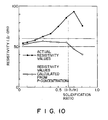
where H is the initial surface level of the melt in the outer crucible, and h is the surface level of the melt in the inner crucible to be kept constant during the pulling process. Therefore, in a case where the floating type double-crucible method is effected by using impurity acting as donor or acceptor to grow crystal having constant resistivity in the longitudinal direction, the resistivity can be kept constant only when the solidification ratio is less than 0.6 to 0.7. If the solidification ratio becomes larger, the resistivity will significantly vary. - Further, it was found that the constant resistivity of the crystal could not be obtained even in the range of the solidification ratio expressed by equation (1) when the floating type double crucible method was effected to be intended to grow crystal having constant and high resistance in its longitudinal direction. This problem occurs when, for example, the low donor (phosphorus P) concentration is used to grow high resistance N-type silicon single crystal with the resistivity of more than 20 0*crn and so the donor concentration is not sufficiently high with respect to the acceptor concentration of boron (B), aluminum (At) or the like flowing out of the quartz crucible. In this case, as shown in Fig. 10, the actual resistivity value (indicated by mark •) gradually increases with increase in the solidification ratio and the resistivity value of the crystal cannot be determined only by the concentration (indicated by mark o) of doped donor impurity (P).
- The inventors of this invention have proposed a pulling apparatus having an integral type double crucible (Japanese Patent Application No. 61-221896, or US Patent Application No. 091,947 filed on September 1, 1987). The pulling apparatus is shown in Fig. 1. In Fig. 1, 11 denotes an outer crucible, and 14 denotes a cylindrical separation wall integrally and coaxially formed with
outer crucible 11. The inner space ofouter crucible 11 is divided intoinner chamber 20 andouter chamber 21 byseparation wall 14.Inner chamber 20 andouter chamber 21 are connected with each other by means ofsmall hole 15 and narrow pipe-like coupling tube 16 formed withsmall hole 15. With this construction, melt ML2 inouter chamber 21 is supplied toinner chamber 20 whilesingle crystal 17 is being pulled from melt ML1 in the inner chamber. - The impurity of melt ML1 in the inner chamber is inhibited from flowing into the outer chamber by the preset length L of
coupling tube 16 not only during the pulling process but also when melt is not transferred fromouter chamber 21 toinner chamber 20. Length L is determined to be larger than four times inner diameter a oftube 16. In this respect, the integral type double crucible is different from the floating type double crucible which has onlyhole 15. - One of the proposed crystal pulling methods using the integral type double crucible is to solve the problem that the impurity concentration in the longitudinal direction of crystal formed by the floating type double crucible method is limited by the solidification ratio used in equation (1). In this case, doped material melt ML1 (impurity concentration Ci) is received in
inner chamber 20 of the integral type double crucible and undoped material melt ML2 is received inouter chamber 21. Further, ratio r/R of radius r ofinner chamber 20 and radius R ofouter chamber 21 is set to be equal to square root /k of segregation coefficient k of the doping impurity andcrystal 17 of impurity concentration kCi is pulled by πR2ΔH (AH is decrease in the surface level of melt ML1) from melt ML1 in the inner chamber. Then, the amount of impurity 7rR2AH x kCi included in a portion ofcrystal 17, which has been grown during the surface level decreases by AH, becomes equal to the amount of impurity πr2ΔH x Ci included within a portion of melt ML1 having width AH so that the impurity concentration of melt ML1 in the inner chamber is kept at constant value Ci during the pulling process. As a result, the impurity concentration in the longitudinal direction ofcrystal 17 can be kept at constant value kci. - Fig. 11 shows the relation between the resistivity (ordinate) and the solidification ratio (abscissa) of single crystal formed by the integral type double crucible method effected in a condition of r/R = √k in comparison with those obtained by the CZ technique and the floating type double crucible method. As shown in Fig. 11, in a case where constant-resistivity crystal is formed by the proposed integral type double crucible method (Japanese Patent Application No. 61-221896 or USSN 091,947), the problem that the solidification ratio is limited by equation (1) in the floating type double crucible method can be solved.
- However, even in the integral type double crucible pulling method, electrically conductive impurity (B, At or the like) flows out of the crucible itself and may cause an inadvertent influence, making it difficult to attain crystal of high and constant resistivity. For example, in a case where two kinds of dopants or two different dopant concentration melts are used, there still remains a problem.
- An object of this invention is to provide a novel crystal pulling method by which substantially 100% of yield with respect to the resistivity of crystal can be attained.
- More specifically, an object of this invention is to provide a crystal pulling method capable of controlling the resistivity in the longitudinal direction of crystal (1) when electrically conductive impurity of the opposite or the same conductivity type is unintentionally introduced into the melt, (2) when two kinds of electrically conductive impurity of the opposite conductivity types are intentionally introduced into the melt, or (3) when melt regions with two different impurity concentration levels of the same conductivity type are intentionally formed.
- The crystal pulling method of this invention for compensating for variation in the characteristic of the pulling crystal due to inadvertent introduction of electrically conductive impurity is effected by using an integral type double crucible. This crucible is divided into
inner chamber 20 andouter chamber 21 by concentric or coaxialcylindrical separation wall 14. In this case, first doped material melt ML1 is received ininner chamber 20 and second undoped material melt ML2 is received inouter chamber 21. - Assume that the segregation coefficient of doping impurity is k, the inner diameter of
inner chamber 20 is 2r, and the inner diameter ofouter chamber 21 is 2R. Then, (r/R) is set to be larger than Vk so as to increase the concentration of the doping impurity in the longitudinal direction of the crystal, thus compensating for the influence by impurity of the opposite conductivity types unintentionally introduced intocrystal 17. Otherwise, (r/R) is set to be smaller than Vk so as to decrease the concentration of the doping impurity in the longitudinal direction of the crystal, thus compensating for the influence by impurity of the same conductivity types unintentionally introduced intocrystal 17. - For example, the influence of changing the resistivity in the longitudinal direction of the crystal by P-type or N-type impurity unintentionally introduced into N-type crystal can be compensated for by intentionally changing the concentration of the N-type doping impurity in the longitudinal direction of the crystal. Thus, the resistivity in the longitudinal direction of the pulling crystal can be controlled.
- For example, suppose that the resistivity of more than 20 Ω'cm is controlled in the longitudinal direction of phosphorus (P) doped N-type high resistance silicon single crystal pulled from a quartz crucible from which acceptor, such as B or Aℓ, flows out of the quartz crucible, and segregation coefficient k is set at 0.35 and therefore √k is 0.59. In this case, the ratio of (r/R) is set to satisfy the condition of 0.85 s (r/R) > 0.59. Selection of the resistivity in the above range can be made by previously detecting the amount of acceptor flowing out of the crucible.
- In general, ratio r/R must be understood as ratio √
Si/(So+Si) when the upper surface area of melt ininner chamber 20 is Si and the upper surface area of melt inouter chamber 21 is So. That is, the above range is determined by using Si/(Si+So) instead of r/R when the crucible and separation wall are not cylindrical. The range must be set to satisfy the condition that
0.85 > √Si/(Si+So) > 0.59, for example. - In another crystal pulling method of this invention, two kinds of conductive impurities of opposite conductivity types are intentionally introduced. In this method, first doped material melt ML1 is received in
inner chamber 20 of the integral type double crucible, and conductive impurity having a conductivity type (P) opposite to the conductivity type (N) of the doped impurity of melt ML1 is introduced into second material melt ML2 inouter chamber 21. The doped impurity concentration of melt ML1, which will become high during the pulling process, is reduced and compensated for by introducing melt ML2 into the inner chamber. The resistivity variation in the longitudinal direction of pulling crystal can thus be controlled. - Assume now that the radius of the outer crucible is R and the
radius separation wall 14 is r. Then, area Si ofinner chamber 20 is πr2, area So ofouter chamber 21 is π(R2-r2), and total area (Si + So) ofcrucible 11 is πrR2. - When the segregation coefficient is x, concentration C4 (x) of impurity A which has been doped into melt ML1 in the inner chamber and has been taken into pulling
crystal 17 can be expressed as follows.

- Further, when the segregation coefficient is x, concentration CB (x) of impurity B which has been doped into melt ML2 in the outer chamber and taken into pulling
crystal 17 can be expressed as follows.


- The effective concentration of impurity A in the crystal with solidification ratio x can be kept at substantially the same value as that of the crystal obtained at the initial pulling stage by such a manner that one of impurity A and impurity B compensates for the other thereof. For this purpose, concentration Cm (0) of impurity B which determines


- If equation (6) is satisfied, the resistivity becomes equal in portions with solidification ratios of 0 and x (0 < x < 0.85). Further, the resistivity in portions with the segregation coefficient other than the portion of x in the solidification ratio can be controlled, so that deviation of the resistivity from a desired value can be suppressed within a relatively narrow range.
- When impurities A and B are of the same conductivity type, the resistivity of the crystal can be kept constant. That is, when the solidification ratio is x, impurity concentration Cs(x) in the pulling crystal can be expressed as follows.


- If impurity is doped to adjust impurity concentration Co(0) of the melt in the outer chamber so as to satisfy the following equation,


- Thus, the impurity concentration in the crystal can be made constant in the longitudinal direction thereof.
- In the method of this invention, a coupling mechanism (15, 16) provided between the inner and outer chambers can be used to suppress the outflow of doped impurity included in melt ML1 in the inner chamber of the integral type double crucible to
outer chamber 21. In this case, it should be noted that the coupling mechanism is not limited to pipe-like tube 16. - This invention can be more fully understood from the following detailed description when taken in conjunction with the accompanying drawings, in which:
- Fig. 1 is a sectional view showing the main portion of a double crucible which can be used in a crystal pulling method according to one embodiment of this invention;
- Fig. 2 is a graph showing the relation between the solidification ratio and the impurity concentration of silicon single crystal obtained by the crystal pulling method according to one embodiment of this invention, with r/R used as a parameter;
- Fig. 3 is a graph showing the relation between the solidification ratio, the resistivity and the impurity concentration of silicon single crystal obtained by the crystal pulling method according to one embodiment of this invention, with r/R set at 0.70;
- Fig. 4 is a graph showing the relation between the solidification ratio, the resistivity and the impurity concentration of silicon single crystal obtained by the crystal pulling method according to one embodiment of this invention, with r/R set at 0.75;
- Fig. 5 is a graph showing the relation between the solidification ratio and the impurity concentration of silicon single crystal obtained by a crystal pulling method other than the crystal pulling method of this invention;
- Figs. 6A to 6F are graphs each showing the relation between the solidification ratio and the impurity concentration of silicon single crystal obtained by the crystal pulling method according to one embodiment of this invention, with r/R used as a parameter;
- Fig. 7 is a graph showing the relation between the solidification ratio and the oxygen concentration of silicon single crystal obtained by the crystal pulling method according to one embodiment of this invention, with r/R used as a parameter;
- Fig. 8 is a graph showing the relation between the solidification ratio and the impurity concentration of silicon single crystal obtained by the crystal pulling method according to one embodiment of this invention, and the relation between the solidification ratio and the impurity concentration of silicon single crystal obtained by a crystal pulling method other than the crystal pulling method of this invention;
- Fig. 9 is a sectional view of the main portion of a floating type double crucible; and
- Figs. 10 and 11 are graphs explaining the problem of the floating type double crucible.
- Now, this invention is explained with reference to an embodiment applied to a silicon single crystal pulling method.
- Fig. 1 shows a crystal pulling apparatus used in one embodiment of this invention. As shown in Fig. 1,
graphite crucible 12 is mounted on vertically movable androtatable crucible shaft 12, andquartz crucible 11 of 12 4) is disposed in close contact with the inner surface ofgraphite crucible 12. Quartzcylindrical separation wall 14 with radius r is coaxially disposed in and bonded tocrucible 11.Hole 15 is formed inseparator wall 14 andquartz pipe 16 which has inner diameter a (= 6 mm) and length L (= 150 mm), andpipe 16 withhole 15 is mounted onwall 14. L is determined to satisfy the condition: 21rr > L ≧ 4a. - With this double crucible,
silicon crystal 17 of 4" φ is pulled from melt ML1 ininner chamber 20 of the crucible which is divided byseparation wall 14. Further, ML2 denotes melt inouter chamber 21. - In the following embodiments using the integral type double crucible, the charge amount of silicon material was 14 kg. Further, when the coupling means is constructed only by means of
small hole 15, supply of dopant impurity toinner chamber 20 orouter chamber 21 is effected after the grown crystal in the stage of the shouldering becomes 10 mmφ and before the straight body thereof, so that reverse flow of the melt frominner chamber 20 toouter chamber 21 is prevented. When the coupling means between the inner and outer chambers is formed of pipe-like passage 16 which has an effect of suppressing the outflow of impurity from inner chamber melt ML1 to outer chamber melt ML2, supply of dopant impurity if effected after material silicon has melted and the surface levels of the melts in the inner and outer chambers have become equal to each other. - In embodiment 1, impurity which is flowed out from the quartz crucible is compensated for and high resistance N-type single crystal having a uniform resistivity of 50 Ω'cm and 100 Ω'cm, which is constant in the longitudinal direction thereof, is pulled. In order to check the concentration of impurity of flowing out of the double crucible (11, 14), inner diameter 2r of the separation wall was variously changed, crystals were grown from the undoped melt (in both the inner and outer chambers), and then the conductivity types and the resistances of the grown crystals were detected and the apparent impurity concentration was derived based on these detected values. As the result, the conductivity type of the flow-out impurity from
crucible body 11 andseparation wall 14 of quartz was detected to be P-type, and the resistivity in the longitudinal direction was detected to decrease from the head portion of 1000 to 2000 Ω'cm to the tail portion of several hundreds Ω'cm. Fig. 2 shows the distribution of the derived impurity concentration. - Ratio r/R was set to 0.70 according to the result of Fig. 2. Phosphorus was doped into melt ML1 in the inner chamber so as to set the resistivity of the crystal head portion to 50 Ω'cm (the concentration of phosphorus is 1 x 10¹⁴- atoms/cc). Melt ML2 in the outer chamber was kept undoped. Under this condition,
single crystal 17 of N-type high resistance was pulled. Fig. 3 shows the distribution of the resistivity and the impurity concentration in the longitudinal direction ofsingle crystal 17. - Fig. 3 indicates that gradually increasing amount of P-type impurity (mark 0) flowing out of the quartz crucible (11, 14) with ratio r/R set at 0.70 and unintentionally doped into
crystal 17, can be compensated for by gradually increasing concentration (mark o) of N-type impurity (P) intentionally doped intocrystal 17 and, consequently, the resistivity (mark •) ofcrystal 17 can be made substantially constant in the longitudinal direction. - Further, single crystal of N-type high resistance having the resistivity of 100 Ω'cm (phosphorus concentration is 0.5 x 10¹⁴ atoms/cc) was pulled with ratio r/R set to 0.75. The result was the same as before and is shown in Fig. 4.
- Fig. 5 shows the distribution of impurity concentration of high resistance silicon single crystal having N-type resistivity of 50 Ω'cm and pulled by use of the quartz floating type double crucible. In this case, even if solidification ratio x is set in the range of 0 < x < 1-(h/H), the effective impurity concentration (mark @) or the resistivity cannot be made constant.
- Further, it was confirmed that the in-plane distribution of the resistivity of a sliced wafer was obtained in which Ap was 5 to 20% in the case of plane orientation (or crystal growing orientation) (111) and Ap was 4 to 10% in the case of plane orientation (100) and these values were the same as those obtained by the CZ technique.
- In this embodiment, phosphorus (N-type impurity: P, its segregation coefficient is 0.35) was doped into melt in
inner chamber 20, boron (P-type impurity: B, its segregation coefficient is 0.80) was doped into melt inouter chamber 21, and N-type siliconsingle crystal 17 with constant resistivity (5 Ω'cm) in the longitudinal direction was pulled while ratio r/R was variously changed. Now, one example of a crystal pulling method in which a double crucible with ratio r/R set to 0.75 was used, is explained in detail. - First, items relating to solidification ratio x was determined as shown in table 1 in order to solve equation (6).

- The boron concentration at the initial pulling stage (solidification ratio is 0) is adjusted based on equation (6) so that excess P (phosphorus) can be compensated for by intentionally introduced B (boron) portion in which the solidification ratio is 0.7 and the effective concentration of phosphorus can be set to be equal to that at the initial pulling stage. That is, Cm (0) is determined to satisfy the following equation.


-


- As seen from table 2, the resistivity can be sufficiently expected to be made constant.
- Figs. 6A to 6F show the results of the verification experiments effected in conditions that ratios r/R were respectively set at 0.60, 0.65, 0.70, 0.75, 0.80, and 0.85; phosphorus and boron were respectively doped into melts in
inner chamber 20 andouter chamber 21, and the effective phosphorus concentration of a portion in which solidification ratio x is 0.70 and that of a portion in which solidification ratio x is 0 were controlled to become equal to each other. From the experiments, it was verified that the resistivity was kept substantially constant at a value of 5 Ω·cm in the longitudinal direction as indicated by the above theory. - As shown in Figs. 6A to 6F, when ratio r/R is set to any value within the range between 0.60 (or 0.59) and 0.85, the resistivity in the longitudinal direction of crystal can be made constant. Therefore, ratio r/R can be set to a proper value which is preferable to a characteristic other than the resistivity. For example, oxygen concentration [Oi] in silicon single crystal becomes high as the diameter of the crucible with respect to that of the crystal becomes smaller.
- Fig. 7 shows oxygen concentration [Oi] in the longitudinal direction of crystals obtained in the above verification experiments. As is clearly seen from Fig. 7, if the specific range of 1.55 to 1.85 x 10'8 atoms/cc is set with respect to [Oi], the specific [Oi] values can be satisfied by setting ratio r/R to 0.70 or 0.75.
- In this embodiment, ratio r/R is set to 0.70, boron is doped into the melts in the inner and outer chambers, and single crystal with the resistivity of 10 Ω·cm and oxygen concentration of 1.55 to 1.85 x 10¹⁸ atoms/cc is grown. For this purpose, equation (9) is solved as follows.


- Further, Ci(0) is the concentration of boron in the melt in the inner chamber at the initial pulling stage, and Co(0) is the concentration of boron in the melt in the outer chamber at the initial pulling stage.
- Crystal was pulled in a condition that boron was doped into the melt in
inner chamber 20 at the concentration of Ci(0) to attain the resistivity of 10 Ω·cm and boron was doped into the melt inouter chamber 21 at a concentration of Co(0) to satisfy equation (12). Then, the single crystal in which the resistivity was constant as shown in Fig. 8 and the oxygen concentration was set within the same specified range as that shown by marks • in Fig. 7 was obtained. - For purposes of comparison, the resistivity of the single crystal obtained by the CZ technique is shown in Fig. 8. As is seen from Fig. 8, the segregation coefficient of boron is 0.80 and is close to 1, and is a dopant which causes the lest variation in the resistivity in the longitudinal direction of crystal. However, when boron is used in the CZ technique, the resistivity will significantly vary from 10 Ω·cm to 7 Ω·cm. In contrast, in this invention, the resistivity can be kept substantially constant, and moreover the oxygen concentration can be set to a desired value.
- According to the novel method of this invention, an integral type double crucible different from that used in the conventional CZ technique or floating type double crucible method is used, and the resistivity in the longitudinal direction of the semiconductor single crystal can be made constant. As a result, (a) it becomes possible to pull crystal with the constant and high resistivity of 50 Ω·cm or 100 Ω·cm which cannot be attained by the conventional method and (b) it is possible to pull crystal by use of two types of impurities or two kinds of melts which impurity concentration levels are different each other. Further, (c) it is possible to control not only the resistivity but also a characteristic such as the oxygen concentration other than the resistivity. The features (a), (b), and (c) can be realized with substantially 100% of yield, and therefore the industrial value of the method of this invention is significantly large.
- Further, according to the present invention, it is possible to grow single crystal having the distribution of the resistivity in the cross sectional direction (perpendicular to the longitudinal direction) of crystal which is different from the distribution of the resistivity of the FZ crystal and is constant as in the distribution of the resistivity of the CZ crystal. Ge or GaAs can be grown instead of Si by this method of invention. Further,
crucible 11 and/orseparation wall 14 can be formed of Pylotic Boron Nitride (PBN), Si3N4, or SiC, or can be formed of quartz coated with PBN, Si3N4, or SiC.
Claims (10)
Applications Claiming Priority (2)
| Application Number | Priority Date | Filing Date | Title |
|---|---|---|---|
| JP42583/88 | 1988-02-25 | ||
| JP63042583A JPH085740B2 (en) | 1988-02-25 | 1988-02-25 | Semiconductor crystal pulling method |
Publications (3)
| Publication Number | Publication Date |
|---|---|
| EP0330189A2 true EP0330189A2 (en) | 1989-08-30 |
| EP0330189A3 EP0330189A3 (en) | 1989-10-25 |
| EP0330189B1 EP0330189B1 (en) | 1992-09-30 |
Family
ID=12640091
Family Applications (1)
| Application Number | Title | Priority Date | Filing Date |
|---|---|---|---|
| EP89103115A Expired - Lifetime EP0330189B1 (en) | 1988-02-25 | 1989-02-22 | Semiconductor crystal pulling method |
Country Status (5)
| Country | Link |
|---|---|
| US (1) | US5073229A (en) |
| EP (1) | EP0330189B1 (en) |
| JP (1) | JPH085740B2 (en) |
| KR (1) | KR920009564B1 (en) |
| DE (1) | DE68903008T2 (en) |
Cited By (4)
| Publication number | Priority date | Publication date | Assignee | Title |
|---|---|---|---|---|
| EP0798403A1 (en) * | 1996-03-27 | 1997-10-01 | Shin-Etsu Handotai Company Limited | Continuously charged czochralski method of manufacturing silicon monocrystal, and dopant feeding apparatus |
| WO2007001184A1 (en) | 2004-12-27 | 2007-01-04 | Elkem Solar As | Method for producing directionally solidified silicon ingots |
| FR2940806A1 (en) * | 2009-01-05 | 2010-07-09 | Commissariat Energie Atomique | SEMICONDUCTOR SOLIDIFICATION METHOD WITH ADDED DOPE SEMICONDUCTOR LOADS DURING CRYSTALLIZATION |
| WO2016179022A1 (en) * | 2015-05-01 | 2016-11-10 | Sunedison, Inc. | Methods for producing single crystal ingots doped with volatile dopants |
Families Citing this family (8)
| Publication number | Priority date | Publication date | Assignee | Title |
|---|---|---|---|---|
| US5312600A (en) * | 1990-03-20 | 1994-05-17 | Toshiba Ceramics Co. | Silicon single crystal manufacturing apparatus |
| DE69428302T2 (en) * | 1993-03-29 | 2002-07-04 | Kabushiki Kaisha Toshiba, Kawasaki | Regulation of the oxygen concentration in a single crystal drawn from a melt containing a Group V element. |
| JP3015656B2 (en) * | 1994-03-23 | 2000-03-06 | 株式会社東芝 | Method and apparatus for producing semi-insulating GaAs single crystal |
| KR100485151B1 (en) * | 2002-08-26 | 2005-04-22 | 주식회사 실트론 | A Grower For Single Crystalline Silicon |
| JP4760729B2 (en) * | 2006-02-21 | 2011-08-31 | 株式会社Sumco | Silicon single crystal wafer for IGBT and manufacturing method of silicon single crystal wafer for IGBT |
| JP5909276B2 (en) * | 2011-05-06 | 2016-04-26 | ジーティーエイティー アイピー ホールディング エルエルシーGtat Ip Holding Llc | Growth of uniformly doped silicon ingot by doping only the first charge |
| US9863062B2 (en) | 2013-03-14 | 2018-01-09 | Corner Star Limited | Czochralski crucible for controlling oxygen and related methods |
| US9822466B2 (en) | 2013-11-22 | 2017-11-21 | Corner Star Limited | Crystal growing systems and crucibles for enhancing heat transfer to a melt |
Family Cites Families (10)
| Publication number | Priority date | Publication date | Assignee | Title |
|---|---|---|---|---|
| FR66315E (en) * | 1906-09-03 | 1956-06-29 | Int Standard Electric Corp | Amplifier devices using semiconductors or crystals |
| GB760778A (en) * | 1953-07-23 | 1956-11-07 | Telefunken Gmbh | Improvements in or relating to the manufacture of single crystals |
| US2892739A (en) * | 1954-10-01 | 1959-06-30 | Honeywell Regulator Co | Crystal growing procedure |
| DE2152801A1 (en) * | 1970-11-09 | 1972-05-10 | Little Inc A | Method and furnace for pulling crystals of uniform composition according to the Czochralski method |
| US4352784A (en) * | 1979-05-25 | 1982-10-05 | Western Electric Company, Inc. | Double crucible Czochralski crystal growth apparatus |
| US4246064A (en) * | 1979-07-02 | 1981-01-20 | Western Electric Company, Inc. | Double crucible crystal growing process |
| JPS6126591A (en) * | 1984-07-18 | 1986-02-05 | Fujitsu Ltd | Crystal growing method |
| JPS6270291A (en) * | 1985-09-19 | 1987-03-31 | Toshiba Corp | Method for producing gaas single crystal and apparatus thereof |
| JPS62226890A (en) * | 1986-03-27 | 1987-10-05 | Komatsu Denshi Kinzoku Kk | Single crystal and its production |
| JPS6379790A (en) * | 1986-09-22 | 1988-04-09 | Toshiba Corp | Crystal pulling up device |
-
1988
- 1988-02-25 JP JP63042583A patent/JPH085740B2/en not_active Expired - Fee Related
-
1989
- 1989-02-22 EP EP89103115A patent/EP0330189B1/en not_active Expired - Lifetime
- 1989-02-22 DE DE8989103115T patent/DE68903008T2/en not_active Expired - Fee Related
- 1989-02-25 KR KR1019890002233A patent/KR920009564B1/en not_active Expired
-
1990
- 1990-06-29 US US07/545,098 patent/US5073229A/en not_active Expired - Lifetime
Cited By (9)
| Publication number | Priority date | Publication date | Assignee | Title |
|---|---|---|---|---|
| EP0798403A1 (en) * | 1996-03-27 | 1997-10-01 | Shin-Etsu Handotai Company Limited | Continuously charged czochralski method of manufacturing silicon monocrystal, and dopant feeding apparatus |
| US5900055A (en) * | 1996-03-27 | 1999-05-04 | Shin-Etsu Handotai Co., Ltd. | Method of manufacturing silicon monocrystal by continuously charged Czochralski method |
| WO2007001184A1 (en) | 2004-12-27 | 2007-01-04 | Elkem Solar As | Method for producing directionally solidified silicon ingots |
| EP1848843A4 (en) * | 2004-12-27 | 2011-09-28 | Elkem Solar As | METHOD FOR THE PRODUCTION OF DIRECTED FIRST STAINED SILICON BARS |
| FR2940806A1 (en) * | 2009-01-05 | 2010-07-09 | Commissariat Energie Atomique | SEMICONDUCTOR SOLIDIFICATION METHOD WITH ADDED DOPE SEMICONDUCTOR LOADS DURING CRYSTALLIZATION |
| EP2208810A1 (en) * | 2009-01-05 | 2010-07-21 | Commissariat à l'énergie atomique et aux énergies alternatives | Method for solidifying a semiconductor with adding charges of a doped semiconductor during the crystallisation |
| WO2016179022A1 (en) * | 2015-05-01 | 2016-11-10 | Sunedison, Inc. | Methods for producing single crystal ingots doped with volatile dopants |
| CN108138354A (en) * | 2015-05-01 | 2018-06-08 | 各星有限公司 | Method for producing single crystal ingot doped with volatile dopant |
| CN108138354B (en) * | 2015-05-01 | 2021-05-28 | 各星有限公司 | Method for producing a single crystal ingot doped with a volatile dopant |
Also Published As
| Publication number | Publication date |
|---|---|
| EP0330189B1 (en) | 1992-09-30 |
| JPH085740B2 (en) | 1996-01-24 |
| KR920009564B1 (en) | 1992-10-19 |
| DE68903008T2 (en) | 1993-04-22 |
| JPH01215789A (en) | 1989-08-29 |
| EP0330189A3 (en) | 1989-10-25 |
| KR890012893A (en) | 1989-09-20 |
| DE68903008D1 (en) | 1992-11-05 |
| US5073229A (en) | 1991-12-17 |
Similar Documents
| Publication | Publication Date | Title |
|---|---|---|
| EP0330189A2 (en) | Semiconductor crystal pulling method | |
| US5515810A (en) | Method and apparatus for manufacturing semi-insulation GaAs monocrystal | |
| US4894206A (en) | Crystal pulling apparatus | |
| EP2705178B1 (en) | Growth of a uniformly doped silicon ingot by doping only the initial charge | |
| US4352784A (en) | Double crucible Czochralski crystal growth apparatus | |
| US5021225A (en) | Crystal pulling apparatus and crystal pulling method using the same | |
| US4911780A (en) | LEC method for growing a single crystal of compound semiconductors | |
| US5034200A (en) | Crystal pulling apparatus and crystal pulling method | |
| EP0388503A1 (en) | Method for pulling single crystals | |
| EP0219966B1 (en) | Process for pulling a crystal | |
| EP4271862B1 (en) | Use of buffer members during growth of single crystal silicon ingots | |
| EP0141495B1 (en) | A method for pulling a single crystal | |
| JP4380204B2 (en) | Silicon single crystal and single crystal growth method | |
| US6254674B1 (en) | Method of controllably delivering dopant by limiting the release rate of dopant from a submerged vessel | |
| US4456499A (en) | Double crucible Czochralski crystal growth method | |
| US5427056A (en) | Apparatus and method for producing single crystal | |
| US5488923A (en) | Method for producing single crystal | |
| US5873938A (en) | Single crystal pulling apparatus | |
| EP1722014A1 (en) | Method for manufacturing nitrogen-doped silicon single crystal | |
| EP0141649B1 (en) | An apparatus for pulling a single crystal | |
| GB2338909A (en) | Heat and interface control during single crystal growth | |
| EP0226794B1 (en) | Method of drawing-up a single crystal using a double-crucible apparatus and double-crucible apparatus therefor | |
| CA1272106A (en) | Double crucible for single crystal growth | |
| JPH0362679B2 (en) | ||
| JPS61158896A (en) | Method for producing compound semiconductor single crystal and apparatus therefor |
Legal Events
| Date | Code | Title | Description |
|---|---|---|---|
| PUAI | Public reference made under article 153(3) epc to a published international application that has entered the european phase |
Free format text: ORIGINAL CODE: 0009012 |
|
| 17P | Request for examination filed |
Effective date: 19890317 |
|
| AK | Designated contracting states |
Kind code of ref document: A2 Designated state(s): DE FR GB |
|
| PUAL | Search report despatched |
Free format text: ORIGINAL CODE: 0009013 |
|
| AK | Designated contracting states |
Kind code of ref document: A3 Designated state(s): DE FR GB |
|
| 17Q | First examination report despatched |
Effective date: 19910604 |
|
| GRAA | (expected) grant |
Free format text: ORIGINAL CODE: 0009210 |
|
| AK | Designated contracting states |
Kind code of ref document: B1 Designated state(s): DE FR GB |
|
| REF | Corresponds to: |
Ref document number: 68903008 Country of ref document: DE Date of ref document: 19921105 |
|
| ET | Fr: translation filed | ||
| PLBE | No opposition filed within time limit |
Free format text: ORIGINAL CODE: 0009261 |
|
| STAA | Information on the status of an ep patent application or granted ep patent |
Free format text: STATUS: NO OPPOSITION FILED WITHIN TIME LIMIT |
|
| 26N | No opposition filed | ||
| PGFP | Annual fee paid to national office [announced via postgrant information from national office to epo] |
Ref country code: FR Payment date: 19970211 Year of fee payment: 9 |
|
| PGFP | Annual fee paid to national office [announced via postgrant information from national office to epo] |
Ref country code: GB Payment date: 19970213 Year of fee payment: 9 |
|
| PGFP | Annual fee paid to national office [announced via postgrant information from national office to epo] |
Ref country code: DE Payment date: 19970228 Year of fee payment: 9 |
|
| PG25 | Lapsed in a contracting state [announced via postgrant information from national office to epo] |
Ref country code: GB Free format text: LAPSE BECAUSE OF NON-PAYMENT OF DUE FEES Effective date: 19980222 |
|
| PG25 | Lapsed in a contracting state [announced via postgrant information from national office to epo] |
Ref country code: FR Free format text: THE PATENT HAS BEEN ANNULLED BY A DECISION OF A NATIONAL AUTHORITY Effective date: 19980228 |
|
| GBPC | Gb: european patent ceased through non-payment of renewal fee |
Effective date: 19980222 |
|
| PG25 | Lapsed in a contracting state [announced via postgrant information from national office to epo] |
Ref country code: DE Free format text: LAPSE BECAUSE OF NON-PAYMENT OF DUE FEES Effective date: 19981103 |
|
| REG | Reference to a national code |
Ref country code: FR Ref legal event code: ST |