EP0329023A2 - Dispositif pour effectuer un traitement numérique du signal comportant des opérations papillon de transformée rapide de Fourier de racine 4 - Google Patents
Dispositif pour effectuer un traitement numérique du signal comportant des opérations papillon de transformée rapide de Fourier de racine 4 Download PDFInfo
- Publication number
- EP0329023A2 EP0329023A2 EP89102276A EP89102276A EP0329023A2 EP 0329023 A2 EP0329023 A2 EP 0329023A2 EP 89102276 A EP89102276 A EP 89102276A EP 89102276 A EP89102276 A EP 89102276A EP 0329023 A2 EP0329023 A2 EP 0329023A2
- Authority
- EP
- European Patent Office
- Prior art keywords
- data
- signal groups
- input
- digital
- complex
- Prior art date
- Legal status (The legal status is an assumption and is not a legal conclusion. Google has not performed a legal analysis and makes no representation as to the accuracy of the status listed.)
- Withdrawn
Links
- 238000012545 processing Methods 0.000 title claims description 13
- 238000000034 method Methods 0.000 claims abstract description 13
- 230000015654 memory Effects 0.000 claims description 66
- 230000004044 response Effects 0.000 claims description 17
- 230000008569 process Effects 0.000 claims description 2
- 230000008878 coupling Effects 0.000 claims 6
- 238000010168 coupling process Methods 0.000 claims 6
- 238000005859 coupling reaction Methods 0.000 claims 6
- 239000000758 substrate Substances 0.000 claims 2
- 101000798429 Pinus strobus Putative 2-Cys peroxiredoxin BAS1 Proteins 0.000 claims 1
- 101001136140 Pinus strobus Putative oxygen-evolving enhancer protein 2 Proteins 0.000 claims 1
- 101000600488 Pinus strobus Putative phosphoglycerate kinase Proteins 0.000 claims 1
- 238000006880 cross-coupling reaction Methods 0.000 claims 1
- 230000009977 dual effect Effects 0.000 description 33
- 230000006870 function Effects 0.000 description 32
- 238000010586 diagram Methods 0.000 description 29
- 230000000295 complement effect Effects 0.000 description 9
- 238000012546 transfer Methods 0.000 description 6
- 241000255777 Lepidoptera Species 0.000 description 5
- 239000000872 buffer Substances 0.000 description 5
- 101001030591 Homo sapiens Mitochondrial ubiquitin ligase activator of NFKB 1 Proteins 0.000 description 4
- 102100038531 Mitochondrial ubiquitin ligase activator of NFKB 1 Human genes 0.000 description 4
- 238000005215 recombination Methods 0.000 description 4
- 230000006798 recombination Effects 0.000 description 4
- 230000003068 static effect Effects 0.000 description 3
- 230000007704 transition Effects 0.000 description 3
- 101000739146 Homo sapiens Protein SFI1 homolog Proteins 0.000 description 2
- 102100037271 Protein SFI1 homolog Human genes 0.000 description 2
- 230000015572 biosynthetic process Effects 0.000 description 2
- 238000013461 design Methods 0.000 description 2
- 230000007246 mechanism Effects 0.000 description 2
- 230000000135 prohibitive effect Effects 0.000 description 2
- 238000012163 sequencing technique Methods 0.000 description 2
- 238000012935 Averaging Methods 0.000 description 1
- 238000003775 Density Functional Theory Methods 0.000 description 1
- 101100365603 Phytophthora infestans (strain T30-4) SFI2 gene Proteins 0.000 description 1
- 238000003491 array Methods 0.000 description 1
- 230000002457 bidirectional effect Effects 0.000 description 1
- 230000008859 change Effects 0.000 description 1
- 238000013480 data collection Methods 0.000 description 1
- 230000003111 delayed effect Effects 0.000 description 1
- 230000001419 dependent effect Effects 0.000 description 1
- 230000000694 effects Effects 0.000 description 1
- 238000001914 filtration Methods 0.000 description 1
- 238000011010 flushing procedure Methods 0.000 description 1
- 239000003292 glue Substances 0.000 description 1
- 230000010354 integration Effects 0.000 description 1
- 238000007620 mathematical function Methods 0.000 description 1
- 239000002184 metal Substances 0.000 description 1
- 230000001343 mnemonic effect Effects 0.000 description 1
- 238000010606 normalization Methods 0.000 description 1
Images


Classifications
-
- G—PHYSICS
- G06—COMPUTING; CALCULATING OR COUNTING
- G06F—ELECTRIC DIGITAL DATA PROCESSING
- G06F9/00—Arrangements for program control, e.g. control units
- G06F9/06—Arrangements for program control, e.g. control units using stored programs, i.e. using an internal store of processing equipment to receive or retain programs
- G06F9/30—Arrangements for executing machine instructions, e.g. instruction decode
- G06F9/30003—Arrangements for executing specific machine instructions
- G06F9/30007—Arrangements for executing specific machine instructions to perform operations on data operands
- G06F9/3001—Arithmetic instructions
- G06F9/30014—Arithmetic instructions with variable precision
-
- G—PHYSICS
- G06—COMPUTING; CALCULATING OR COUNTING
- G06F—ELECTRIC DIGITAL DATA PROCESSING
- G06F17/00—Digital computing or data processing equipment or methods, specially adapted for specific functions
- G06F17/10—Complex mathematical operations
- G06F17/14—Fourier, Walsh or analogous domain transformations, e.g. Laplace, Hilbert, Karhunen-Loeve, transforms
- G06F17/141—Discrete Fourier transforms
- G06F17/142—Fast Fourier transforms, e.g. using a Cooley-Tukey type algorithm
-
- G—PHYSICS
- G06—COMPUTING; CALCULATING OR COUNTING
- G06F—ELECTRIC DIGITAL DATA PROCESSING
- G06F9/00—Arrangements for program control, e.g. control units
- G06F9/06—Arrangements for program control, e.g. control units using stored programs, i.e. using an internal store of processing equipment to receive or retain programs
- G06F9/30—Arrangements for executing machine instructions, e.g. instruction decode
- G06F9/30003—Arrangements for executing specific machine instructions
- G06F9/30007—Arrangements for executing specific machine instructions to perform operations on data operands
- G06F9/30036—Instructions to perform operations on packed data, e.g. vector, tile or matrix operations
Definitions
- the Discrete Fourier Transform (DFT) is commonly used in a variety of Digital Signal Processing (DSP) Systems.
- DSP Digital Signal Processing
- FFT Fast Fourier Transform
- Two VLSI devices are described for applications in high performance FFT and other DSP systems. Both devices will utilize 1.2 u CMOS dual-level-metal process.
- CE Computational Element
- MC Micro Controller
- Extremely fast and self contained systems can be designed by combining CE and MC devices with off-the-shelf memory devices. The system performance can be traded against choosing the number of CEs, MCs and memory devices in a given system.
- the chip-set can implement FFT systems ranging from 4 complex-points to 64K complex-points.
- a 1024 complex-point FFT for example, can be performed in 20 microseconds (us) using the disclosed hardware.
- the CE is a highly integrated, application specific, semi-programmable, computational device containing several multipliers, adders and registers.
- the device can perform a variety of FFT-specific and general purpose DSP operations, including logical operations at extremely high speed. For example, a radix-4 butterfly or, a block of four complex-multiples, can be performed in 80 ns (the machine cycle of the computational element) in a pipelined mode.
- the machine cycle of the device which is specified to be 80 ns, is termed Tm.
- the device accepts two sets of four ccmplex-data values and produces one set of four complex-data values every machine cycle, in a pipelined mode.
- Its block floating point 16 bit parallel architecture is optimized to implement following FFT specific functions on a single chip:
- CE has a variety of general purpose functions available such as Block-Add, Block-Subtract, Block-AND, Block-EXOR. These functions operate on blocks of four complex values every machine-cycle.
- the dual I/O CE is configured around four data buses called D1, D2, D3 and D4. It also has two auxiliary data input buses AXD1 and AXD2 for feeding twiddle (scaling and constant) factors, etc. At any time, the pair D1 and D2 could be receiving the data while the pair D3 and D4 could be outputting data. The role of this pair of buses could be reversed at any machine cycle via an instruction.
- the dual I/O CE accepts a complex value every Tm/4 ns, over each pair of its input buses. Therefore, a set of four complex values are inputted every Tm ns over input bus pairs. Similarly, the device outputs a complex value on its pair of output buses every Tm/4 ns, producing a set of four complex values every Tm ns.
- Tm 80 ns
- the quad I/O version of the CE will be available in a larger package.
- the quad I/O CE which is shown in Figure 1.1, contains four data input buses (D1, D2, D5, D6) and four data output buses (D3, D4, D7, D8).
- the twiddle factors, etc. are fed over four auxiliary buses AXD1, AXD2, AXD3, AXD4.
- each bus is operated at a rate of 25 MHz since the number of buses have been doubled.
- four real inputs are fed to the device.
- the corresponding four imaginary inputs are fed in the latter half of the machine cycle.
- the outputs are produced in the same sequence on the output buses.
- the role of the input and output buses can not be reversed in the quad I/O mode.
- the dual I/O version of the CE could be used to design very flexible FFT and other DSP systems by using off-the-shelf single-port memories. This flexibility is possible because the dual I/O CE transfers one complex value at a time, the real and imaginary part of which are stored at the same address. In addition, its lower pin count (144 pin package) makes it very attractive for system design. Initially, the device can be packaged in a PGA package and a surface mount version will be made available at a later stage. On the other hand, quad version of the CE is attractive due to somewhat relaxed memory access time. However, it leads to a larger package (244 pins) which makes it prohibitive in a surface mount package at this time. Also, a four port memory system may be required when standard FFT algorithms are used because it deals with parts of four complex numbers at a time.
- both versions of the CE have identical internal data paths.
- a series of magnitude-detectors are provided at the output data stages of the CE which continuously monitor the upper 6 bits of the output data array for FFT operations.
- a scaling factor is produced after processing a column of N complex-point data array. The scaling factor is used to scale the data array on the input stage of the next pass by the input scalers (shift and round mechanism), included on the chip. It protects the CE adders from overflowing during the computation by providing conditional scaling.
- An accumulated scale factor is available at the beginning of each pass, which should be effectively treated as an exponent for the normalization of the processed array of data. The scheme is referred to as Block Floating Point in the literature.
- the FFT Micro Controller is a device which provides all the addressing sequences required to address the memory devices associated with an FFT system.
- the MC is intended to be a companion device for the dual I/O version of the CE device for FFT applications only. It generates the necessary addressing sequences and control signals for the dual I/O CE and associated memories minimizing external glue logic.
- Typical FFT systems can be built by using the CE, the MC and off-the-shelf memories.
- the MC is designed to generate the following addressing sequences supporting FFT systems up to 64K complex-points.
- a computational element responsive to control signals, for performing a plurality of digital signal processing operations on the elements of an operand array.
- the computational element can perform a fast Fourier transform radix-4 butterfly computation on four complex operands every 80 ns in a pipelined mode.
- the computational element can be configured to perform two sets of fast Fourier transform radix-2 butterfly computations.
- the computational element can be further configured to perform arithmetic and logic operations on an operand array.
- the computational element can be configured to perform a plurality of sequential operations on an operand array or can be configured to perform one of a sequence of operations when coupled in series with at least one other computational element.
- the computational element of the present invention can be fabricated on a single chip using integrated circuit techniques.
- a microcontroller, providing control signals and constant factors for computation to the computational element can be fabricated on a second chip.
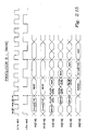
- a block diagram of the MC is shown in Figure 1.2 illustrating various buses and control signals.
- the device produces five 16 bit address outputs, labeled as IA(15:0), D1A(15:0), AXA(15:0), D2A(15:0) and OA(15:0).
- Each bus produces addresses at a rate of 50 MHz, matching the speed of dual I/O CE device.
- the IA bus produces sequential addresses needed to collect the input data while previous data is being transformed.
- the D1A and D2A buses produce read-data and write-data addresses corresponding to the FFT algorithm.
- the read-address and the write-address patterns are the same but separated by a latency-factor associated with the CE and the rest of the system.
- the twiddle factor memory (auxiliary data memory) address sequence is produced on the AXA bus.
- a sequential or digit-reversed address can be produced on the OA bus to read the output data memory, containing previously transformed data.
- the device produced various signals to control external bus-drivers, memory and the CE.
- the device also has a host interface to communicate to a host microprocessor or a control memory.
- the host processor could use the IA bus as an address bus to address internal registers during initialization. The corresponding data is transferred over D1A bus in this case. If a host processor is not employed in the system, the MC is capable of down loading itself from an external memory for stand-alone applications. Following are some of the registers of the MC which are down loaded initially:
- the instruction register file contains a set of instructions to implement the desired FFT system configuration.
- a normal FFT system is composed of multiple "PASSES" of the N complex-point numbers through the CE; the PASSES being windowing, FFT nodes, Square-Sum, etc.
- One instruction per PASS is executed by the MC to appropriately manage the external memories and the CE.
- Each instruction contains information such as the following:
- the MC is packaged in a 132 pin package, dissipating less than 500 mW.
- the device is available in a PGA package.
- a surface mount version will be made available at a later stage.
- the MC and the CE can be used in a variety of system configurations providing various trade-offs between performance, hardware and cost. Following are some of the system configurations which could be produced by using the CE and the MC.
- the CE can be used in a variety of non-FFT systems by using the system architectures discussed here.
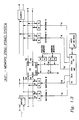
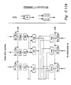
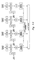
- a N complex-point FFT system is shown in Figure 1.3 which is based upon a dual ping-pong memory architecture. Independent input and output buffer memories have been included for real time operation. At a given instance, while new data is being collected in memory A, previously transformed data is being read from output memory D. The IA and OA buses of MC supply the input and output memory addresses respectively. Meanwhile, current data is being transformed by the CE, supported by dual memories B and C. The data flows in a ping-pong fashion between memories B anc C for multiple passes. Each pass of the N complex-point data can perform full windowing, or one column of the FFT, or square-summing, etc. At each pass, address buses of the MC can be programmed to switch in a ping-pong fashion.
- the CE is also capable of interchanging its input/output data ports. Therefore, minimum external bus multiplexers are required. After a complete transform, the external data buses are switched around to interchange the role of the memories. It takes log4(N) passes through the CE to perform a N complex-point FFT using a radix-4 algorithm. Additional passes are needed for windowing and square/summing if so desired. Note that each pass takes memory cycles (N/4 machine cycles). A memory cycle is defined to be a read or a write operation.
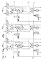
- FIG. 1.4 shows a cascaded FFT system, illustrating M nodes.
- the first node is an input node performing windowing operation.
- the last node is an output node dedicated to square-summing.
- Intermediate nodes are dedicated to the FFT algorithm, each node corresponding to a column of FFT.
- Each FFT system node is double buffered with N complex-point data memories so that data flows through the CE as described in the previous section but in one direction. After completing each pass, the paired buffer memories are interchanged, maintaining a data flow from left to right continuously.
- Each MC can be programmed to switch internally the addresses on the buses D1A and D2A, etc. to match the interchanging of the memories at the end of each pass.
- the performance of such a FFT system corresponds to the time taken for one N complex-point pass (N memory cycles).
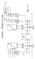
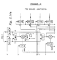
- FIG. 1.5 A block diagram of such a system is shown in Figure 1.5.
- Two additional memory systems have been included for the data-input and data-output maintaining a real-time operation. At any time, only one memory is connected to the CE. Both the read and the write operations have to be performed to that memory for every complex-point of data (two memory cycles).
- the MC automatically manages address buses for alternate read and write operations. It takes approximately 2N memory cycles for every pass of N complex-point data. Therefore, a total of 2N of log 4(N) memory cycles will be required for a N complex-point FFT.
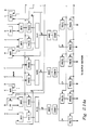
- the lower-end system can be collapsed to minimum hardware configuration by discarding the input and output memories as shown in Fig 1.6.
- the MC can be programmed first to collect the input data in the data RAM. Then, data can be processed by making multiple passes through the CE. Finally, the data can be output to an external device.
- the MC can be programmed to generate all the address sequences on the D1A bus. The performance of such a system is similar to the previous system. However, additional time will be taken for the input and output operations.
- a summary of FFT system performance, based on the CEs and the MCs is given in Table 1.1.
- the mid-range system offers a middle compromise between the amount of hardware and performance. It requires one CE, one MC, 24 memory chips and few bus drivers to implement a real-time FFT system, including the input/output data memories.
- the application of CE and MC is not limited to the system configurations here. Many other higher performance and intermediate performance configurations are possible due to the programmable nature of the MC and CE.
- the MC has been primarily designed to support the dual I/O CE for in-place, DIF, radix-4/radix-2 FFT systems.
- the MC is capable of producing four addresses per machine-cycle/per address-bus.
- four strobe signals have been provided to latch those four addresses into external registers in a machine cycle.
- the external registers could be used to address a four-port memory system, supporting the quad I/O CE.
- the Computational Element can be viewed as a very high performance, semi-programmable, application-specific, vector processor which operates on arrays of data at very high speed. Although it has been primarily designed for FFT and related systems, its semi-programmable architecture lends itself in a variety of other DSP applications such as FIR filters, DFTs, complex-modulation/demodulation, etc. Its programmability, performance and cost-effectiveness allows it to be used for implementing time-domain DSP systems by using frequency-domain DSP techniques. The CE also has the capability of very high speed logical operations which makes it useful for systems such as graphics and image processing.
- the CE integrates multiple multipliers, adders, registers, magnitude detectors, etc. on a single chip. It has multiple high-performance, parallel inputs and parallel outputs to maintain data-flow from external parallel devices to the on-chip processor. All the on-chip resources could be kept busy for the applications mentioned earlier.
- the device achieves the computation rate close to one Giga Operations Per Second (GOPS) in a pipelined mode.
- GOPS Giga Operations Per Second
- An operation is defined to be a multiplication, an addition or an equivalent operation.
- the device operates at an I/O data rate close to 5 Gigabits Per Second to maintain data flow to the processor.
- Table 2.0 The key features of the CE are shown in Table 2.0.
- the CE operates on complex values. Therefore, all the values on the CE are described in a complex format.
- the simplest way of handling real numbers on the CE is by setting imaginary parts of complex values to zero. When imaginary parts are also used as real values, extreme care should be taken.
- the CE uses fractional, two's complement format throughout for the arithmetic operations. For logical operations, the real and imaginary parts of a complex value contain independent logical values. Following are the formats used in the architecture of the CE for the representation of various operands:
- Computational Rate up to one GIGA-OPERATIONS per second (1 GOPS).
- the Data I/O Rate up to 5 Giga Bits Per Second.
- the FFT-specific and general-purpose functions executed every 80 ns.
- a single-chip integration of vector-functions such as FFT Radix-4 butterfly, block multiply, block-add, block-logical functions, etc. Every 80 ns, operates upon 4 complex-data values and 4 complex auxiliary-data values, and produces 4 complex data values. For example: 1024 complex-point FFT executed in about 20 ⁇ s.
- FIG. 2.0 A block diagram of the CE, emphasizing data inputs, auxiliary data inputs, data outputs and pipeline stages is shown in Figure 2.0. As shown in the Figure, all the buses are 16 bits wide to directly interface to parallel memory devices.
- the processors of the CE may be programmed to implement several different functions as described later. Basically, the processor has been designed to operate upon two sets of four complex values, each set consisting of four 16 bit complex values. After a pipeline latency, the processor produces a set of four 16 bit complex values as an output. As shown in the Figure 2.0, the latency from the input to the output is four machine cycles due to the pipeline register stages RO, R1, R2, and R6. Effectively, these registers are clocked at the machine cycle rate.
- the machine cycle time is defined to be an interval during which all four complex operands are fed to the device.
- the machine cycle time is specified to be 80 ns for the CE. Subsequently, the machine cycle time will be referred to an Tm nanoseconds.
- the processor accepts two sets of four complex numbers every machine cycle and produces one set of four complex numbers every machine cycle at the output stage.
- FIG. 2.0 four 16 bit input complex data operands are switched into a set of eight 16-bit registers R0[7:0](15:0), from external input D buses during a machine cycle time Tm.
- R0[7:0](15:0) stands for a set of eight 16 bit registers.
- the individual registers, in-turn are called R01(15:0), R02(15:0), etc.
- a corresponding input set of four 16-bit complex auxiliary data operands are switched into another set of eight 16 bit registers called RX0[7:0](15:0), from external input AXD buses.
- the Processor B produces additional latency of one machine cycle due to internal pipelining. This latency is shown by including an additional stage of registers in the Processor B in Fig. 2.0.
- the results (a set of four 16 bit complex values) are latched into a set of output registers R6[7:0](15:0) on the following machine-cycle.
- the values are fed to the output data buses during this machine-cycle over a period of Tm. Therefore, latency of four machine cycles results from the input to the output of the CE.
- the CE operates at a machine-cycle time of Tm ns.
- faster clocks are required to input and output all the values within a machine-cycle.
- each bus operates at a rate of 4/Tm MHz, transferring a 16-bit word every Tm/4 ns.
- a CLKIN signal of 4/Tm MHz is needed in the dual I/O mode to handle bus transfers. Every Tm/4 ns, each pair of buses carries corresponding real and imaginary parts of a complex number.
- CONFIG input pin
- the CE has to work at half the speed in this case (machine cycle time of 2Tm ns) to allow read and write sequentially.
- CONFIG pin is set at a logic high level
- the CLKIN signal is internally divided by a factor of two to slow down the CE.
- either the bus pair D1/D2 or the bus pair D3/D4 is used for both the read and write operations, as shown in Fig 2.3.
- the bus pair is dynamically switched by the external DIR signal for alternate read and write operations. The timing will be further clarified in the following sections.
- the external buses can be reconfigured by putting a logic high signal on the BM pin.
- this mode which is called the quad mode
- the CE bus configuration appears as shown in Figure 2.4.
- Each set of four complex numbers is transferred over corresponding set of four buses instead of two buses in the dual I/O mode.
- the buses D1, D2, D5 and D6 carry the four input complex-data values and the buses AXD1, AXD2, AXD3 and AXD4 carry the four auxiliary input complex-data values.
- the buses D3, D4, D7 and D8 carry the four output complex-data values.
- the bus-direction pin DIR and the CONFIG pin are in the Don't Care mode in this case. Therefore, the directionality of the buses can not be changed in the quad I/O mode.
- each bus Since twice the number of buses are available to transfer each set of four complex numbers, each bus operates at half the rate compared to the dual I/O mode.
- the buses operate at a rate of 25 MHz, transferring a 16 bit value every Tm/2 ns in the quad I/O mode.
- real parts of four complex numbers are transferred over corresponding four buses in the first half of the machine cycle.
- the four corresponding imaginary parts are transferred in the later part of the machine cycle, completing a transfer of four complex numbers.
- a model of the internal clock generator of the CE is shown in Fig 2.5.
- the clock generator is activated by a CLKIN signal from an external pin.
- the CLKIN signal is fed with a 4/Tm MHz clock or a 2/Tm MHz clock, depending upon the input BM signal. If the device is in a quad I/O mode, the input frequency must be 4/Tm MHz.
- the input clock rate must be 2/Tm MHz, if the device is in a quad I/O mode.
- the clock generator is further controlled by the input CONFIG signal.
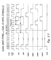
- the clock generator In the dual I/O mode, when CONFIG input is zero, the clock generator generates internal clocks which are called CK2, CK4, CK8, CK8PO, CK8P1, CK8P2 and CK8P3 as shown in Fig 2.6.
- An external signal, SYNC is used to synchronize the internal CE clocks with internal clocks of other external devices which share the same SYNC and CLKIN signals.
- the CLKIN is fed at a frequency of 4/Tm MHz, which produces the CK4 signal at 2/Tm MHz and the CK8 signal at 1/Tm MHz.
- the CK8P0 to CK8P3 are four non-overlapping quarter phases of the CK8 signal.
- the signal CK8 appears at the CLKOUT output pin of the CE.
- the clock generator goes into a reset mode, taking various clock outputs to a low level as shown in Fig 2.6.
- the SYNC signal makes a transition from high to low, the CK4 and CK8 signals make a transition to logic high on the first following positive transition of CK2.
- the clock generator When CONFIG is set to a high level, the clock generator produces clock waveforms as shown in Fig 2.7. Although, the CLKIN signal is at a frequency of 4/Tm MHz, all the internal waveforms are slowed down by a factor of two due to an internal division of the CLKIN signal by two.
- the SYNC signal maintains synchronization with the CLKIN signal as described before.
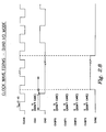
- the clock waveforms appear as shown in Fig 2.8.
- the CK4, CK8P0, CK8P1, CK8P2 and CK8P3 are in the Don't care state.
- the SYNC signal operates, as before, in synchronism with the CLKIN signal which is fed at a frequency of 2/Tm MHz.
- Fig 2.5 is a model of the clock generator. The actual implementation on the chip is different. On the chip, minimum skew is achieved between CLKIN and various internal clocks. The clock signals shown in this section will be used throughout these specifications in order to clarify the timing of various elements.
- the device operates on a set of four single precision, complex data values and a set of four single precision, complex auxiliary data values, every machine cycle. It produces a set of four single precision, complex data values every machine cycle as an output.
- Data Input Operand O r0 + j i0
- Data Input Operand 1 r1 + j i1
- Data Input Operand 2 r2 + j i2
- Data Input Operand 3 r3 + j i3
- r# and i# are respectively the real and the imaginary parts of input single-precision complex numbers.
- the j is the square root of the negative unity.
- (r+ji)[3:0] The set of four input data operands will be referred to as (r+ji)[3:0] in the future.
- (c+ji)[3:0] is a set of four input auxiliary data operands as following.
- Auxiliary Data Input Operand 0: c0 + j s0 Auxiliary Data Input operand 1: c1 + j s1
- (x+jy)[3:0] is defined to be a set of single precision, complex, output data values produced by the CE as following.
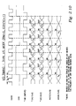
- FIG. 2.9 A timing diagram, showing the timing of various input/output operands, which have been defined in the previous section, is shown in Fig 2.9 for the dual I/O mode when CONFIG pin is held in a low state.
- the buses are operated four times per machine cycle as mentioned before. Note that, for example, the value (r0 + j i0) is fed in first and the value (r3 + j i3) is fed in at the end of a machine cycle.
- the various I/O time slots (within a machine cycle) on various buses are referred to as "ro slot", "io slot”, "ao slot”, etc.
- the CLKIN is at a frequency of 4/Tm MHz and the machine cycle is stretched to Tm/2 ns.
- Alternate read and write operations are performed over the bidirectional bus pair either D1/D2, or D3/D4.
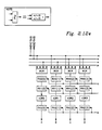
- the bus directionality is controlled by an external signal DIR as shown in the Figure 2.10.
- DIR signal is applied in accordance with the timing relationships shown, the CE is responsible for providing correct output data and clocking in the correct data.
- the Figure 2.10 shows the timing of data buses D1 and D2. Instead, if buses D3 and D4 are used, the polarity of the applied signal DIR must be reversed.
- the I/O timing for the quad I/O mode is shown in Fig. 2.11. As mentioned above, the device uses all the buses in this mode and each bus is operated at a rate of 2/Tm MHz as shown in Fig 2.11. Note that four real parts of a set of complex numbers are transferred during the first half of the machine cycle. The corresponding four imaginary parts are transferred during the second half of the machine cycle.
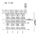
- the I/O architecture of the CE is shown in the block diagram of Fig 2.12.
- the device has a set of 8 input/output data buses D[8:1](15:0) and a set of 4 input auxiliary data buses AXD[4:1](15:0) as discussed previously.
- the buses could be used in the dual or quad I/O mode.
- the device has a set of four input buses which are called IB[4:1](15:0).
- IB[4:1](15:0) receives a set of four input data values (r+ji)[3:0] every machine-cycle over external data buses.
- the values are received over internal bus pair IB1/IB2 or over four buses IB1bI/IB2/IB3/IB4, depending upon the BM pin. All together, eight values are clocked in (four real and four imaginary).
- the in-coming data is channeled through input multiplexers to a set of eight 16 bit registers which are called RO[7:0](15:0). It is assumed that every register, shown in the architecture of CE, is clocked on a positive edge.
- Each in-coming data value (r0, i0, r2, i2, etc.) is assigned to one of the RO# registers.
- the pattern of assignment of various members of the input set of data values (r+ji)[3:0] to various members of the set of registers R0[7:0] may change from instruction to instruction.
- An instruction is a group of logical values, applied on six input pins INS(5:0), as shown in control block of Fig 2.12.
- An instruction configures the Processor A and Processor B to execute various functions described earlier (Butterfly, Block-Multiply, etc).
- the instruction-set is summarized below and a detailed account of each instruction is presented.
- Each instruction requires the input set of data (r+ji)[3:0] in a different sequence in the input registers of the Processor A. Therefore, the assignment of input data values to register set R0 changes from instruction to instruction as stated earlier. This is achieved by controlling the input multiplexers and the sequence of clocks to various members of register set R0[7:0] as the input data comes in.
- the R0[7:0] registers are fed with the clock-set CK8P(3:0) or by CK8/CK8- depending upon the BM mode. All the eight input data values are clocked into R0[7:0] register-set within a machine cycle in a sequence defined by the instruction being executed.
- the data is clocked into the next set of registers R1[7:0](15:0) by CK8 in the next machine cycle, making it available for the Processor A.
- the Processor A executes on the data, depending upon the instruction, and results are latched into a set of registers R2[7:0](15:0) which are further processed by the Processor B.
- auxiliary data In parallel with data, a set of four input auxiliary data values, (c+js)[3:0], is collected over a set of internal auxiliary input buses, XIB[3:1](15:0).
- the bus pair XIB1/XIB2 or all the four buses XIB[3:1] may be used depending upon the I/O modes.
- the auxiliary data is clocked into a set of input auxiliary registers RX0[7:0](15:0) using the multiplexers and controlling the clock-inputs to the registers. Again, the assignment of input auxiliary values to the registers RX0[7:0] may vary from instruction to instruction.
- All the eight values, (c+js)[3:0], are clocked into the register set RX0[7:0] over a machine cycle in a sequence defined by the instruction.
- the values are moved to the register set RX1[7:0](15:0) by CK8 signal.
- the auxiliary data is further delayed by a machine cycle by moving it into the next set of registers, RX2[7:0](15:0), by CK8 signal.
- a series of 'one bit right shift and round' circuits have been included in between each member of the register-set RX1[7:0] and the corresponding member of register-set RX2[7:0].
- Each input auxiliary value may be shifted by one bit to the right by controlling the XSIN pin.
- a Round bit, RNDX is added to the lsb of the shifted value to perform unbiased rounding.
- the RNDX is determined by the following logical equation.
- RNDX DB1 . DB0 where DB0 is the discarded lsb bit and DB1 is the next higher significant bit. Note that when logical instructions are implemented, the shift is logical and no rounding is performed.
- register-set RX2[7:0] When auxiliary data is clocked into register-set RX2[7:0], it gets aligned with the data contained by the register set R2[7:0]. Both register-sets feed the data to the Processor B for further computation.
- the Processor B which causes an additional latency of one machine-cycle due to its internal pipelining, produces a set of values (x+jy)[3:0] in the register set R6[7:0](15:0).
- the processor B assigns various members of the set (x+jy)[3:0] to various registers in the set R6[7:0], in different ways for different instructions.
- the CE has a variety of programmable input/output options which have been described so far.
- the Processor A and Processor B may be programmed to execute a variety of instructions as shown in Table 2.2.
- BFLY4 A Radix-4, DIF, FFT Butterfly.
- BFLY 2 Two Radix-2, DIF, FFT Butterflies
- FFT2N Recombine N Complex Point FFT to 2N Real Point
- FFTNN Recombine N Complex Point FFT to two N Real Point FFTs.
- BMUL Block multiply two sets of complex numbers.
- BSQSM Block Square/Sum a set of complex numbers.
- BADD Block Add two sets of complex numbers
- BCONJ Block Conjugate a set of complex numbers
- BCONS Block of Constants produce ZERO or ONE on outputs.
- the instruction bits I(5:0) (Table 2.2) are defined at the input pins of the device.
- the Primary Function of an instruction is defined by the bits I(3:0).
- the bit I4 is called CI which stands for Conjugate-Input or Complement-Input.
- the bit CI which is active high, is used to conjugate, arithmetically-complement or logically-complement the incoming data values.
- the functionality of the CI depends upon the Class of instructions. In FFT Class, the CI is used for conjugate control. All the incoming complex data values are conjugated by two's complementing the imaginary parts before operations are performed by the instruction.
- the CI acts as a global two's complement control. All the incoming complex values (real and imaginary) are two's complemented before the values are operated upon.
- the CI also acts as complement control for the logical Class of instructions. However, in this case, all the incoming values are logically complemented (inverted) before the operation, defined by the instruction, is performed.
- the CO bit behaves in a similar fashion for three classes of instructions, except that conjugate or complement operation is performed at the output. First the operation, defined by the instruction, is performed. Then, the outgoing data is conjugated or complemented. Note that the CI impacts the incoming data through the data-input section only. It does not impact the auxiliary input data.
- the conjugate control along with FFT instructions, can be used to implement inverse FFTs.
- the conjugate facility also allows the implementation of time-domain filtering by using frequency domain techniques.
- the complementing facilities, along with the instructions in the Arithmetic Class and the Logical Class, provides additional functionality for a variety of applications.
- An instruction much be set-up one machine-cycle in advance of the data. Typically, the instruction will remain static for processing a block of N complex values.
- the processor A derives its inputs from the register set R2[7.0].
- the processor A is basically dedicated to perform initial summing operations associated with various FFT oriented instructions (BFLY4, BFLY2, FFT2N, etc) which are shown in the instruction description.
- FFT oriented instructions BFLY4, BFLY2, FFT2N, etc
- general purpose instructions such as BMUL, BADD, BXOR
- the processor A is basically in the flow-through mode to pass the data to the processor B.
- FIG.13 A block diagram of the processor A is shown in Fig 2.13.
- the eight inputs to the processor A are first passed through a set of two's complementers, designated as COMO-COM7 in Figure 2.13.
- the complementers are directly controlled by the input pins COMP(7:0) or by the I4 bit in the instruction, depending upon the SPLM (SPECIAL MODE) pin and the class of effective instruction.
- SPLM SPECIAL MODE
- each Complementer is directly controlled by the values on pins COMP(7:0), for FFT class of instructions. For example, if COMPO is high, then complementer COMO, produces a two's complement when data passes through it. If COMPO is low then data passing through COMO is unaffected.
- complementers COM1-COM7 are affected by the values on pins COMP1-COMP7.
- pin SPLM is in a low state, the complementers are not affected by inputs COMP(7:0). Instead the bit I4 (Conjugate Input - CI) controls the input complementers.
- I4 Conjugate Input - CI
- I4 Conjugate Input - CI
- the data is passed through a set of Shift and Round circuits, designated as SRO-SR7 in Fig 2.13.
- the SR blocks produce a shift on incoming data as defined by pins SFI(2:0). All the SR blocks produce the same amount of shift.
- the sign bit is extended into the most significant bit (msb) positions if arithmetic instruction is being implemented, otherwise, zeros are inserted in the msb positions.
- Table 2.3 describes the SFI(3:0) inputs and the produced shift.
- RND (SFI2-. SFI1 -. SFI0 . DB1 . DB0) + (SF2- . SF1 . SF0- . DB1 . [DBO +DB2]) + (SF2- . SF1 . SFO . DB2 [DBO + DB1 + DB3]) + (SF2 . SF1- . SF0- . DB3 . [DBO + DB1 + DB2 + DB4])
- DBO to DB4 are unshifted data bits; the bit DBO being the least significant bit (lsb).
- the RND bit is forced to be a zero when logical instructions are implemented.
- the data passes through a first set of adder stages, designated as PS0 to PS7 (Programmable Summers) in Fig 2.13.
- PS8-PS15 The values are further combined by a second stage of Programmable Summers, called PS8-PS15.
- a Programmable Summer is an adder, containing programmable inputs as shown in the notation of Fig 2.13. Either input of a PS can be two's complemented. Either or both inputs may also be programmed to be zero, disregarding the incoming data. In this way, a PS can be used to add, subtract, flow-through or produce zeros.
- the PS are automatically programmed by the instruction bits I(3:0) as described in the instruction descriptions.
- the output from the second PS stage is directly latched into the R2[7:0] register-set.
- the interconnections of PS devices have been determined to implement various FFT instructions. However, data flows through unaffected for other instructions.
- the Processor A produces a set of four single-precision, complex values. Let us define those values to be a set (m+jm)[3:0]. The value (m0+jn0) is contained by the register-pair R20 and R21; m0 being contained by register R20, and n0 being contained by R21. Similarly, the remaining values are contained by the remaining registers in the same sequence.
- the Processor B operates upon two sets of complex numbers, a set (m+jn)[3:0] contained by R2[7:0] registers, and a set (c+js) [3:0] contained by RX2[3:0] registers.
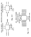
- a block diagram of the Processor B is shown in Fig 2.14.
- the Processor B has been defined to work at twice the speed of Processor A, operating twice in a machine cycle.
- the Processor B contains eight 16 x16 multipliers, four 20 bit ALUs and several pipeline registers.
- the internal pipeline registers of the Processor B are clocked by the 2/Tm MHz clock, CK4, due to the processor cycle-time of Tm/2 ns.
- the processor is organized to perform four complex multiplications in one machine cycle.
- the two multipliers and one ALU is interconnected to form one 'Arm' of the Processor, as shown in Fig 2.14. All the four Arms shown in Fig 2.14 are identical except the highlighted data paths.
- the highlighted data paths allow ALU0 to be able to feed the data to ALU1.
- the ALU2 can send the data to the ALU3.
- Those 'special' paths are used by only one instruction, FFT2N. In the normal mode (when all other instructions are executed), the four Arms appear identical as seen by ignoring highlighted data paths in Fig 2.14. For those instructions, all the Arms are identical and independent. This is called 'normal' mode of operation. When, FFT2N instruction is executed, it uses the 'special' mode of operation.
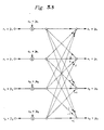
- dashed lines indicate the flow of operands through Processor A and Processor B for the radix-4, decimation-in-frequency, fast Fourier transform, using the butterfly algorithm (BFLY4 in Table 2.2).
- the illustrated flow paths are the same for both phases of the algorithm implementation.
- the input and output paths for the operands and for the algorithm constants pass through the apparatus shown in Fig. 2.11, only the output path varying between the phases.
- the similar operand flow diagrams can be provided for each of the algorithms described in Table 2.2.
- each Arm (Fig. 2.14) has data paths to execute a complex multiply operation in one machine-cycle.
- the Arm 0 operates on two input complex-numbers, (m0+jn0) and, say, (c0+js0). Both input numbers remain stable for a complete machine-cycle, Tm ns, in respective registers R2# and RX2#.
- Tm ns a complete machine-cycle
- the multiplexers of MULO and MUL1 are configured to produce m0.c0 and n0.s0, respectively.
- the products are left justified, truncated to 20 bits, and latched into registers R30 and R31 which are clocked by a CK4 clock.
- the products are transferred to registers R40 and R41, which are clocked by CK4.
- the ALU0 performs a function (m0.c0 - no.s0) which is the real part of the complex multiplication.
- the computed value is rounded to 16 bits, then passed through a two's complementer COMPO, and, then, latched into an intermediate register R50.
- the multiplexers of MULO and MUL1 are switched in the second half of the machine cycle.
- MUL0 and MUL1 produce n0.c0 and m0.s0, respectively.
- the ALUO performs a function (n0.c0 + m0.s0), which is an imaginary part of the output.
- the result is latched into register R61 by a CK8 signal.
- the corresponding output real-term, residing in the register R50 is latched into register R60. Therefore, registers R60 and R6(1) contain results of a complex multiplication, which have been termed (x0+jy0) previously, as an output.
- the timing of the Arm is further clarified in the timing diagram of Fig 2.15. Note that the registers R3# and R4# produce an additional latency of one machine-cycle. This latency has been shown by including a stage of artificial CK8 pipeline registers in the equivalent diagram of the Processor B in Fig 2.0.
- the multiplexers of MUL0 and MUL1 have provisions to produce m0**2 and n0**2, which can be further added by ALU0 to execute a SQSUM instruction.
- the input data can also be passed through the multipliers unaffected by selecting a'1' on the multiplexers.
- the data then can be operated upon by using the ALU.
- the ALU supports various functions such as Add with either input complemented, Logical AND, Logical OR, Logical EXOR, One's Complement, as required by various instructions.
- the Processor B operates in a different mode, called Paired Mode, when the instruction FFT2N is executed, which is described in the next section.
- Arm-0 and Arm-1 are interconnected together by using the highlighted path, as shown in Fig 2.14.
- Arm-2 and Arm-3 are interconnected.
- These data paths are used by the instruction FFT2N as described in its description in the next chapter. In this mode, only one complex-value is produced as an output, by Arm-1 and Arm-3.
- ALU0-ALU3 implement arithmetic instructions (Fig 2.14)
- their outputs are rounded to 16 bits.
- the output of each ALU is first truncated to 16 bits and, then, a bit RNDB is added.
- the RNDB is determined by the following logical equation to perform unbiased rounding.
- RNDB DB2 . [ DB0 + DB1 + DB3 ] Note that DB0 - DB3 are the discarded bits on truncation, the DB0 being the lsb.
- the CE is a pipelined device as mentioned earlier. All the input/output signals have been carefully pipelined so that the pipelining does not cause any inconvenience to the user.
- the data pipelining have been well explained above. The pipelining of various signals is described in relation to the input/output data.
- I/O signals of the CE can be divided into separate categories, as discussed below.
- All these signals are sampled into CE on a positive-going edge of the 1/Tm(CK8) clock. Due to the internal pipelining of these signals, to match the data pipeline, the data can be applied in the next machine cycle, without having to wait for the propagation of those signals to all the pipeline stages. These signals can be changed to start a different pass, while the data corresponding to a previous pass is still flushing through the pipe. Although, in typical applications, these signals will be changed after the data for a current pass is flushed through the chip.
- EOP and BOP are static signals, which typically remain static on pins for the whole pass. Therefore, these signals are called Pass-Static.
- the BOP and EOP are pulsed signals which are activated only once during each Pass. These are called Pass-Pulsed signals.
- the EOP and BOP are sampled on the positive edge of the 1/Tm clock. The EOP and BOP should not exceed the machine-period of the CE.
- I/O data buses have been already set-up as desired, depending upon the external system configuration.
- the following parameters will be used to make reference to the I/O data values which have been defined previously: Data Input Values: r0 + j io, rl + j il, r2 + j i2, r3 + j i3.
- DESCRIPTION The instruction executes two FFT, Radix-2, Decimation-in-Frequency butterflies.
- the x0+jy0 and x1+jy1 become corresponding outputs.
- the r2+ji2 and r3+ji3 become inputs for the second butterfly.
- the x2+jy2 and x3+jy3 become corresponding outputs.
- the c1+js1 and c3+js3 are twiddle-factors for respective butterflies. The user must ensure above mentioned values for c0, s0, c2 and s2 are supplied.
- DESCRIPTION The instruction recombines a FFT of N complex-points into a FFT of 2N real-points. (Reference: The Fast Fourier Transform, E. Oran Brigham, Prentice-Hall, 1974, p.167). Data Input Values: r0 + j i0, Don't Care, r2 + j i2, Don't Care. Auxiliary Input Values: Don't Care, Don't Care, Don't Care, Don't Care. Output Data Values: x0 + j y0, Don't Care, Don't Care, Don't Care, Don't Care
- DESCRIPTION The instruction recombines a FFT of N complex-points into two separate N real-point FFTs.
- Reference The Fast Fourier Transform, E. Oran Brigham, Prentice-Hall, 1974, p. 166).
- Data Input Values r0 + j io, r1 + j i1, r2 + j i2, r3 + j i3.
- Auxiliary Input Values Don't Care, Don't Care, Don't Care, Don't Care.
- DESCRIPTION The instruction passes a set of four complex values from the input to the output of the device. If desired, values may be complemented (negated) during the Pass.
- Data Input Values r0 + j i0, r1 + j i1, r2 + j i2, r3 + j i3.
- DESCRIPTION The instruction multiplies members of a block of four complex values with corresponding members of another block of four complex values.
- Data Input Values r0 + j i0, r1 + j i1, r2 + j i2, r3 + j i3.
- Auxiliary Input Values c0 + j s0, c1 + j s1, c2 + j s2, c3 + j s3.
- the instruction operates on eight data values. It squares each data value and, then, adds pairs together.
- the instruction can be used to compute magnitude-square if input data values are complex. If real, then the instruction can be used to square and sum a data-array by using an off-chip accumulator.
- the input values are 16 bit, single precision values. It produces four 20 bit, extended precision, values.
- the corresponding x and y outputs are combined to represent a 20 bit value.
- the x0 and y0 are used to represent the first 20 bit output value.
- the msb 16 bits are represented by the x0 and the 4 lbs bits are represented by the y0 value.
- the 4 bits are contained by the most significant part of the y0 value.
- the lower 12 bits of the y0 are invalid.
- the values (x1, y1), (x2, y2) and (x3 and y3) are generated in the same way.
- Data Input Values r0, i0; r1, i1; r2, i2; r3, i3.
- Auxiliary Input Values Don't Care; Don't Care; Don't Care; Don't Care.
- DESCRIPTION The instruction adds members of a block of four complex values with corresponding members of another block of four complex values.
- Data Input Values r0 + j i0, r1 + j i1, r2 + j i2, r3 + j i3.
- Auxiliary Input Values c0 + j s0, c1 + j s1, c2 + j s2, c3 + j s3.
- DESCRIPTION The instruction subtracts members of a block of four complex values from corresponding members of another block of four complex values.
- Data Input Values r0 + j io, r1 + j i1, r2 + j i2, r3 + j i3.
- Auxiliary Input Values c0 + j s0, c1 + j s1, c2 + j s2, c3 + j s3.
- DESCRIPTION The instruction conjugates a set of four complex values. If desired, values may be further complemented (negated) at the output.
- Data Input Values r0 + j io, r1 + j i1, r2 + j i2, r3 + j i3.
- Auxiliary Input Values Don't Care, Don't Care, Don't Care, Don't Care.
- DESCRIPTION The instruction produces a block of constants at the output, disregarding the inputs.
- the values of constants may be zero or one.
- Data Input Values Don't Care, Don't Care, Don't Care, Don't Care.
- Auxiliary Input Values Don't Care, Don't Care, Don't Care, Don't Care.
- DESCRIPTION The instruction conjugates the members of a block of four complex values and, then, multiplies those members with corresponding members of another block of four complex values.
- Data Input Values r0 + j i0, r1 + j i1, r2 + j i2, r3 + j i3.
- Auxiliary Input Values c0 + j s0, c1 + j s1, c2 + j s2, c3 + j s3.
- DESCRIPTION The instruction passes a set of four complex values from the input to the output of the device. If desired, values may be logically inverted during the Pass.
- Data Input Values r0, i0; r1, i1; r2, i2; r3, i3.
- Auxiliary Input Values Don't Care, Don't Care, Don't Care, Don't Care.
- DESCRIPTION The instruction logically ANDs the members of a block of four complex values with corresponding members of another block of four complex values.
- Data Input Values r0, i0; r1, i1; r2, i2; r3, i3.
- Auxiliary Input Values c0, s0; c1, s1; c2, s2; c3, s3.
- DESCRIPTION The instruction logically ORs the members of a block of four complex values with corresponding members of another block of four complex values.
- Data Input Values r0, i0; r1, i1; r2, i2; r3, i3.
- Auxiliary Input Values c0, s0; c1, s1; c2, s2; c3, s3.
- DESCRIPTION The instruction logically Exclusive-ORs the members of a block of four complex values with corresponding members of another block of four complex values.
- Data Input Values r0, i0; r1, i1; r2, i2; r3, i3.
- FIG. 3.2 A variation on the architecture which is configured as shown in Figure 3.2, could also be implemented.
- the detailed implementation of such architecture will be similar to that described in this specification.
- the processor A and processor B (see Figures 2.12, 2.13 and 2.14) can be interchanged to achieve such implementation.
- the resulting architecture will be extremely useful for implementing the majority of functions discussed previously.
- the butterfly implementations will follow the decimation-in-time algorithm which is shown in Figure 3.3.
Applications Claiming Priority (2)
| Application Number | Priority Date | Filing Date | Title |
|---|---|---|---|
| US155671 | 1988-02-16 | ||
| US07/155,671 US5303172A (en) | 1988-02-16 | 1988-02-16 | Pipelined combination and vector signal processor |
Publications (2)
| Publication Number | Publication Date |
|---|---|
| EP0329023A2 true EP0329023A2 (fr) | 1989-08-23 |
| EP0329023A3 EP0329023A3 (fr) | 1989-11-02 |
Family
ID=22556328
Family Applications (1)
| Application Number | Title | Priority Date | Filing Date |
|---|---|---|---|
| EP89102276A Withdrawn EP0329023A3 (fr) | 1988-02-16 | 1989-02-10 | Dispositif pour effectuer un traitement numérique du signal comportant des opérations papillon de transformée rapide de Fourier de racine 4 |
Country Status (4)
| Country | Link |
|---|---|
| US (1) | US5303172A (fr) |
| EP (1) | EP0329023A3 (fr) |
| JP (1) | JPH01309173A (fr) |
| CA (1) | CA1308488C (fr) |
Cited By (7)
| Publication number | Priority date | Publication date | Assignee | Title |
|---|---|---|---|---|
| EP0478128A2 (fr) * | 1990-08-10 | 1992-04-01 | General Electric Company | Processeur pipeline de calcul d'une transformation rapide de Fourier |
| GB2283592A (en) * | 1992-12-23 | 1995-05-10 | Duraisamy Sundararajan | Computational structures for the frequency-domain analysis of signals and systems |
| WO1997027550A2 (fr) * | 1996-01-24 | 1997-07-31 | Adc Telecommunications, Inc. | Systeme de communication avec transmission telephonique par porteuses multiples |
| WO1997048197A3 (fr) * | 1996-05-20 | 1997-12-18 | Adc Telecommunications Inc | Systeme de communication a transport telephonique par ondes porteuses multiples |
| EP0875839A1 (fr) * | 1997-05-02 | 1998-11-04 | Sony Corporation | Calculation des transformées de Fourier rapides |
| EP0942379A1 (fr) * | 1998-03-13 | 1999-09-15 | Alcatel | Processeur pipeline de calcul d'une transformation rapide de Fourier |
| WO2009014291A1 (fr) * | 2007-07-26 | 2009-01-29 | Industry-Academic Cooperation Foundation, Yonsei University | Procédé de transformation de fourier rapide et processeur pour système wlan mimo-ofdm 4x4 |
Families Citing this family (58)
| Publication number | Priority date | Publication date | Assignee | Title |
|---|---|---|---|---|
| US5845093A (en) * | 1992-05-01 | 1998-12-01 | Sharp Microelectronics Technology, Inc. | Multi-port digital signal processor |
| US5448169A (en) * | 1993-12-10 | 1995-09-05 | Varian Associates, Inc. | Pulsed FT NMR employing fast combination scaler for faster operation |
| US5481488A (en) * | 1994-10-21 | 1996-01-02 | United Microelectronics Corporation | Block floating point mechanism for fast Fourier transform processor |
| US7280564B1 (en) | 1995-02-06 | 2007-10-09 | Adc Telecommunications, Inc. | Synchronization techniques in multipoint-to-point communication using orthgonal frequency division multiplexing |
| USRE42236E1 (en) | 1995-02-06 | 2011-03-22 | Adc Telecommunications, Inc. | Multiuse subcarriers in multipoint-to-point communication using orthogonal frequency division multiplexing |
| US5943242A (en) * | 1995-11-17 | 1999-08-24 | Pact Gmbh | Dynamically reconfigurable data processing system |
| US7266725B2 (en) | 2001-09-03 | 2007-09-04 | Pact Xpp Technologies Ag | Method for debugging reconfigurable architectures |
| US5793323A (en) * | 1996-11-25 | 1998-08-11 | The United States Of America As Represented By The Secretary Of The Air Force | Two signal monobit electronic warfare receiver |
| DE19651075A1 (de) | 1996-12-09 | 1998-06-10 | Pact Inf Tech Gmbh | Einheit zur Verarbeitung von numerischen und logischen Operationen, zum Einsatz in Prozessoren (CPU's), Mehrrechnersystemen, Datenflußprozessoren (DFP's), digitalen Signal Prozessoren (DSP's) oder dergleichen |
| DE19654593A1 (de) * | 1996-12-20 | 1998-07-02 | Pact Inf Tech Gmbh | Umkonfigurierungs-Verfahren für programmierbare Bausteine zur Laufzeit |
| US6338106B1 (en) | 1996-12-20 | 2002-01-08 | Pact Gmbh | I/O and memory bus system for DFPS and units with two or multi-dimensional programmable cell architectures |
| DE19654595A1 (de) | 1996-12-20 | 1998-07-02 | Pact Inf Tech Gmbh | I0- und Speicherbussystem für DFPs sowie Bausteinen mit zwei- oder mehrdimensionaler programmierbaren Zellstrukturen |
| ATE243390T1 (de) | 1996-12-27 | 2003-07-15 | Pact Inf Tech Gmbh | Verfahren zum selbständigen dynamischen umladen von datenflussprozessoren (dfps) sowie bausteinen mit zwei- oder mehrdimensionalen programmierbaren zellstrukturen (fpgas, dpgas, o.dgl.) |
| DE19654846A1 (de) | 1996-12-27 | 1998-07-09 | Pact Inf Tech Gmbh | Verfahren zum selbständigen dynamischen Umladen von Datenflußprozessoren (DFPs) sowie Bausteinen mit zwei- oder mehrdimensionalen programmierbaren Zellstrukturen (FPGAs, DPGAs, o. dgl.) |
| DE19704044A1 (de) * | 1997-02-04 | 1998-08-13 | Pact Inf Tech Gmbh | Verfahren zur automatischen Adressgenerierung von Bausteinen innerhalb Clustern aus einer Vielzahl dieser Bausteine |
| DE19704728A1 (de) * | 1997-02-08 | 1998-08-13 | Pact Inf Tech Gmbh | Verfahren zur Selbstsynchronisation von konfigurierbaren Elementen eines programmierbaren Bausteines |
| US6542998B1 (en) * | 1997-02-08 | 2003-04-01 | Pact Gmbh | Method of self-synchronization of configurable elements of a programmable module |
| DE19704742A1 (de) * | 1997-02-11 | 1998-09-24 | Pact Inf Tech Gmbh | Internes Bussystem für DFPs, sowie Bausteinen mit zwei- oder mehrdimensionalen programmierbaren Zellstrukturen, zur Bewältigung großer Datenmengen mit hohem Vernetzungsaufwand |
| US5963164A (en) * | 1997-08-15 | 1999-10-05 | The United States Of America As Represented By The Secretary Of The Air Force | Monobit kernel function electronic warefare receiver for characterizing two input signals |
| US5917737A (en) * | 1997-08-15 | 1999-06-29 | The United States Of America As Represented By The Secretary Of The Air Force | Fourier transform mechanization using one bit kernel function |
| US8686549B2 (en) | 2001-09-03 | 2014-04-01 | Martin Vorbach | Reconfigurable elements |
| US6333743B1 (en) | 1997-10-23 | 2001-12-25 | Silicon Graphics, Inc. | Method and apparatus for providing image and graphics processing using a graphics rendering engine |
| DE19861088A1 (de) | 1997-12-22 | 2000-02-10 | Pact Inf Tech Gmbh | Verfahren zur Reparatur von integrierten Schaltkreisen |
| DE19807872A1 (de) | 1998-02-25 | 1999-08-26 | Pact Inf Tech Gmbh | Verfahren zur Verwaltung von Konfigurationsdaten in Datenflußprozessoren sowie Bausteinen mit zwei- oder mehrdimensionalen programmierbaren Zellstruktur (FPGAs, DPGAs, o. dgl. |
| US6078632A (en) * | 1998-04-15 | 2000-06-20 | The United States Of America As Represented By The Secretary Of The Air Force | Minimalized decommunication of serialized telemetry data |
| US6230177B1 (en) * | 1998-06-12 | 2001-05-08 | Silicon Graphics, Inc. | Method and apparatus for performing fast fourier transforms |
| AU5805300A (en) | 1999-06-10 | 2001-01-02 | Pact Informationstechnologie Gmbh | Sequence partitioning in cell structures |
| US6609140B1 (en) | 1999-11-30 | 2003-08-19 | Mercury Computer Systems, Inc. | Methods and apparatus for fast fourier transforms |
| EP1342158B1 (fr) | 2000-06-13 | 2010-08-04 | Richter, Thomas | Protocoles et communication d'unites de configuration de pipeline |
| US20040015899A1 (en) * | 2000-10-06 | 2004-01-22 | Frank May | Method for processing data |
| US8058899B2 (en) | 2000-10-06 | 2011-11-15 | Martin Vorbach | Logic cell array and bus system |
| US7595659B2 (en) | 2000-10-09 | 2009-09-29 | Pact Xpp Technologies Ag | Logic cell array and bus system |
| US6990555B2 (en) * | 2001-01-09 | 2006-01-24 | Pact Xpp Technologies Ag | Method of hierarchical caching of configuration data having dataflow processors and modules having two- or multidimensional programmable cell structure (FPGAs, DPGAs, etc.) |
| US9037807B2 (en) | 2001-03-05 | 2015-05-19 | Pact Xpp Technologies Ag | Processor arrangement on a chip including data processing, memory, and interface elements |
| US7444531B2 (en) | 2001-03-05 | 2008-10-28 | Pact Xpp Technologies Ag | Methods and devices for treating and processing data |
| US7581076B2 (en) | 2001-03-05 | 2009-08-25 | Pact Xpp Technologies Ag | Methods and devices for treating and/or processing data |
| US7210129B2 (en) | 2001-08-16 | 2007-04-24 | Pact Xpp Technologies Ag | Method for translating programs for reconfigurable architectures |
| US7844796B2 (en) | 2001-03-05 | 2010-11-30 | Martin Vorbach | Data processing device and method |
| US7010558B2 (en) * | 2001-04-19 | 2006-03-07 | Arc International | Data processor with enhanced instruction execution and method |
| US7657877B2 (en) | 2001-06-20 | 2010-02-02 | Pact Xpp Technologies Ag | Method for processing data |
| US7996827B2 (en) | 2001-08-16 | 2011-08-09 | Martin Vorbach | Method for the translation of programs for reconfigurable architectures |
| US7434191B2 (en) * | 2001-09-03 | 2008-10-07 | Pact Xpp Technologies Ag | Router |
| US8686475B2 (en) | 2001-09-19 | 2014-04-01 | Pact Xpp Technologies Ag | Reconfigurable elements |
| US7577822B2 (en) | 2001-12-14 | 2009-08-18 | Pact Xpp Technologies Ag | Parallel task operation in processor and reconfigurable coprocessor configured based on information in link list including termination information for synchronization |
| EP1483682A2 (fr) | 2002-01-19 | 2004-12-08 | PACT XPP Technologies AG | Processeur reconfigurable |
| EP2043000B1 (fr) | 2002-02-18 | 2011-12-21 | Richter, Thomas | Systèmes de bus et procédé de reconfiguration |
| US8914590B2 (en) | 2002-08-07 | 2014-12-16 | Pact Xpp Technologies Ag | Data processing method and device |
| AU2003286131A1 (en) | 2002-08-07 | 2004-03-19 | Pact Xpp Technologies Ag | Method and device for processing data |
| US7657861B2 (en) | 2002-08-07 | 2010-02-02 | Pact Xpp Technologies Ag | Method and device for processing data |
| JP4388895B2 (ja) | 2002-09-06 | 2009-12-24 | ペーアーツェーテー イクスペーペー テクノロジーズ アクチエンゲゼルシャフト | リコンフィギュアラブルなシーケンサ構造 |
| EP1426872A3 (fr) * | 2002-12-03 | 2006-02-22 | STMicroelectronics Ltd. | Calcul de FFT/IFFT linéairement scalable dans un système multiprocesseurs |
| EP1447752A3 (fr) * | 2003-02-17 | 2006-02-22 | STMicroelectronics Pvt. Ltd | Procédé et dispositif de calcul de FFT/IFFT multiprocesseur à communication interprocesseurs minimale |
| EP1676208A2 (fr) * | 2003-08-28 | 2006-07-05 | PACT XPP Technologies AG | Dispositif et procede de traitement de donnees |
| WO2007062327A2 (fr) * | 2005-11-18 | 2007-05-31 | Ideal Industries, Inc. | Connecteur de fils liberable |
| EP1974265A1 (fr) | 2006-01-18 | 2008-10-01 | PACT XPP Technologies AG | Procédé de définition de matériels |
| US9606803B2 (en) * | 2013-07-15 | 2017-03-28 | Texas Instruments Incorporated | Highly integrated scalable, flexible DSP megamodule architecture |
| US9600901B2 (en) | 2014-12-22 | 2017-03-21 | International Business Machines Corporation | Video tracker having digital signal processor |
| US9977116B2 (en) * | 2015-10-05 | 2018-05-22 | Analog Devices, Inc. | Scaling fixed-point fast Fourier transforms in radar and sonar applications |
Citations (2)
| Publication number | Priority date | Publication date | Assignee | Title |
|---|---|---|---|---|
| FR2484672A1 (fr) * | 1980-06-13 | 1981-12-18 | Labo Cent Telecommunicat | Module de calcul et dispositif de calcul l'utilisant pour la determination de la transformee de fourier discrete d'une suite d'echantillons |
| US4689762A (en) * | 1984-09-10 | 1987-08-25 | Sanders Associates, Inc. | Dynamically configurable fast Fourier transform butterfly circuit |
Family Cites Families (8)
| Publication number | Priority date | Publication date | Assignee | Title |
|---|---|---|---|---|
| US3777131A (en) * | 1972-02-08 | 1973-12-04 | Westinghouse Electric Corp | High base multiple rail fourier transform serial stage |
| US3800130A (en) * | 1973-07-09 | 1974-03-26 | Rca Corp | Fast fourier transform stage using floating point numbers |
| JPS597990B2 (ja) * | 1976-10-06 | 1984-02-22 | 日本電気株式会社 | N点離散的フ−リエ変換演算装置 |
| US4241411A (en) * | 1978-11-16 | 1980-12-23 | Probe Systems, Incorporated | FFT Parallel processor having mutually connected, multiple identical cards |
| US4393468A (en) * | 1981-03-26 | 1983-07-12 | Advanced Micro Devices, Inc. | Bit slice microprogrammable processor for signal processing applications |
| US4563750A (en) * | 1983-03-04 | 1986-01-07 | Clarke William L | Fast Fourier transform apparatus with data timing schedule decoupling |
| JPS61196370A (ja) * | 1985-02-27 | 1986-08-30 | Yokogawa Medical Syst Ltd | フ−リエ変換装置 |
| NL8502008A (nl) * | 1985-07-12 | 1987-02-02 | Philips Nv | Ontvanginrichting voor het onder bescherming van een stoorsignaal/spraaksignaalbewakingsfunctie herkennen van een aantal verschillende en voorafbepaalde frequentiecombinaties van toonfrequente signaleringscomponenten. |
-
1988
- 1988-02-16 US US07/155,671 patent/US5303172A/en not_active Expired - Lifetime
-
1989
- 1989-02-10 EP EP89102276A patent/EP0329023A3/fr not_active Withdrawn
- 1989-02-14 CA CA000590954A patent/CA1308488C/fr not_active Expired - Lifetime
- 1989-02-15 JP JP8935986A patent/JPH01309173A/ja active Pending
Patent Citations (2)
| Publication number | Priority date | Publication date | Assignee | Title |
|---|---|---|---|---|
| FR2484672A1 (fr) * | 1980-06-13 | 1981-12-18 | Labo Cent Telecommunicat | Module de calcul et dispositif de calcul l'utilisant pour la determination de la transformee de fourier discrete d'une suite d'echantillons |
| US4689762A (en) * | 1984-09-10 | 1987-08-25 | Sanders Associates, Inc. | Dynamically configurable fast Fourier transform butterfly circuit |
Non-Patent Citations (2)
| Title |
|---|
| ELECTRONIC DESIGN * |
| WESCON CONFERENCE RECORD * |
Cited By (17)
| Publication number | Priority date | Publication date | Assignee | Title |
|---|---|---|---|---|
| EP0478128A2 (fr) * | 1990-08-10 | 1992-04-01 | General Electric Company | Processeur pipeline de calcul d'une transformation rapide de Fourier |
| EP0478128A3 (en) * | 1990-08-10 | 1993-12-22 | Gen Electric | Pipelined fast fourier transform processor |
| GB2283592A (en) * | 1992-12-23 | 1995-05-10 | Duraisamy Sundararajan | Computational structures for the frequency-domain analysis of signals and systems |
| GB2283592B (en) * | 1992-12-23 | 1998-10-14 | Duraisamy Sundararajan | FFT butterfly arithmetic units |
| US8638655B2 (en) | 1994-09-26 | 2014-01-28 | Htc Corporation | Systems and method for orthogonal frequency divisional multiplexing |
| US8547824B2 (en) | 1994-09-26 | 2013-10-01 | Htc Corporation | Systems and methods for orthogonal frequency divisional multiplexing |
| US8576693B2 (en) | 1995-02-06 | 2013-11-05 | Htc Corporation | Systems and method for orthogonal frequency division multiplexing |
| WO1997027550A2 (fr) * | 1996-01-24 | 1997-07-31 | Adc Telecommunications, Inc. | Systeme de communication avec transmission telephonique par porteuses multiples |
| WO1997027550A3 (fr) * | 1996-01-24 | 1998-03-05 | Adc Telecommunications Inc | Systeme de communication avec transmission telephonique par porteuses multiples |
| US6434583B1 (en) | 1996-05-20 | 2002-08-13 | Adc Telecommunications, Inc. | Fast fourier transform apparatus and method |
| WO1997048197A2 (fr) * | 1996-05-20 | 1997-12-18 | Adc Telecommunications, Inc. | Systeme de communication a transport telephonique par ondes porteuses multiples |
| WO1997048197A3 (fr) * | 1996-05-20 | 1997-12-18 | Adc Telecommunications Inc | Systeme de communication a transport telephonique par ondes porteuses multiples |
| US6240062B1 (en) | 1997-05-02 | 2001-05-29 | Sony Corporation | Fast fourier transform calculating apparatus and fast fourier transform calculating method |
| EP0875839A1 (fr) * | 1997-05-02 | 1998-11-04 | Sony Corporation | Calculation des transformées de Fourier rapides |
| US6330580B1 (en) | 1998-03-13 | 2001-12-11 | Alcatel | Pipelined fast fourier transform processor |
| EP0942379A1 (fr) * | 1998-03-13 | 1999-09-15 | Alcatel | Processeur pipeline de calcul d'une transformation rapide de Fourier |
| WO2009014291A1 (fr) * | 2007-07-26 | 2009-01-29 | Industry-Academic Cooperation Foundation, Yonsei University | Procédé de transformation de fourier rapide et processeur pour système wlan mimo-ofdm 4x4 |
Also Published As
| Publication number | Publication date |
|---|---|
| US5303172A (en) | 1994-04-12 |
| CA1308488C (fr) | 1992-10-06 |
| JPH01309173A (ja) | 1989-12-13 |
| EP0329023A3 (fr) | 1989-11-02 |
Similar Documents
| Publication | Publication Date | Title |
|---|---|---|
| EP0329023A2 (fr) | Dispositif pour effectuer un traitement numérique du signal comportant des opérations papillon de transformée rapide de Fourier de racine 4 | |
| JP2744526B2 (ja) | 準16基数プロセッサおよび方法 | |
| US4393468A (en) | Bit slice microprogrammable processor for signal processing applications | |
| JP3749022B2 (ja) | 高速フーリエ変換を用いて短い待ち時間でアレイ処理を行う並列システム | |
| US5081573A (en) | Parallel processing system | |
| EP0083967B1 (fr) | Circuit monolithique pour transformée de Fourier rapide | |
| JPH02210538A (ja) | 集積回路と演算処理システム | |
| JP2001520775A (ja) | 算術プロセッサ | |
| JPH02504682A (ja) | 変換処理回路 | |
| Slade | The fast fourier transform in hardware: A tutorial based on an FPGA implementation | |
| JPS6125188B2 (fr) | ||
| US5034910A (en) | Systolic fast Fourier transform method and apparatus | |
| US6463451B2 (en) | High speed digital signal processor | |
| WO2002091221A2 (fr) | Generateur d'adresses pour processeur de transformation de fourier rapide | |
| WO2013097217A1 (fr) | Procédé de calcul papillon de fft parallèle multi-granularité et dispositif correspondant | |
| US7653676B2 (en) | Efficient mapping of FFT to a reconfigurable parallel and pipeline data flow machine | |
| JPS63501828A (ja) | マルチゾ−ンプロセツサ | |
| EP1538533A2 (fr) | Processeur FFT/IFFT amélioré | |
| Towers et al. | Cascadable NMOS VLSI circuit for implementing a fast convolver using the Fermat number transform | |
| Hazarika et al. | Low-complexity continuous-flow memory-based FFT architectures for real-valued signals | |
| Covert | A 32 point monolithic FFT processor chip | |
| Kallapu et al. | DRRA-based Reconfigurable Architecture for Mixed-Radix FFT | |
| JP2697619B2 (ja) | Nポイントfft専用プロセッサ | |
| Karwoski | Four-cycle butterfly arithmetic architecture | |
| Marsh et al. | TM-66 swiFFT DSP chip: architecture, algorithms, and applications |
Legal Events
| Date | Code | Title | Description |
|---|---|---|---|
| PUAI | Public reference made under article 153(3) epc to a published international application that has entered the european phase |
Free format text: ORIGINAL CODE: 0009012 |
|
| AK | Designated contracting states |
Kind code of ref document: A2 Designated state(s): DE FR GB NL |
|
| PUAL | Search report despatched |
Free format text: ORIGINAL CODE: 0009013 |
|
| AK | Designated contracting states |
Kind code of ref document: A3 Designated state(s): DE FR GB NL |
|
| 17P | Request for examination filed |
Effective date: 19900430 |
|
| RAP1 | Party data changed (applicant data changed or rights of an application transferred) |
Owner name: SIGNAL PROCESSING TECHNOLOGIES, INC. |
|
| RAP1 | Party data changed (applicant data changed or rights of an application transferred) |
Owner name: ARRAY MICROSYSTEMS, INC. |
|
| 17Q | First examination report despatched |
Effective date: 19930119 |
|
| STAA | Information on the status of an ep patent application or granted ep patent |
Free format text: STATUS: THE APPLICATION IS DEEMED TO BE WITHDRAWN |
|
| 18D | Application deemed to be withdrawn |
Effective date: 19950204 |