EP0326004B1 - Circuit for sensing the state of matrix cells in MOS EPROM memories - Google Patents
Circuit for sensing the state of matrix cells in MOS EPROM memories Download PDFInfo
- Publication number
- EP0326004B1 EP0326004B1 EP89100780A EP89100780A EP0326004B1 EP 0326004 B1 EP0326004 B1 EP 0326004B1 EP 89100780 A EP89100780 A EP 89100780A EP 89100780 A EP89100780 A EP 89100780A EP 0326004 B1 EP0326004 B1 EP 0326004B1
- Authority
- EP
- European Patent Office
- Prior art keywords
- cell
- current
- circuit
- virgin
- sensing
- Prior art date
- Legal status (The legal status is an assumption and is not a legal conclusion. Google has not performed a legal analysis and makes no representation as to the accuracy of the status listed.)
- Expired - Lifetime
Links
- 239000011159 matrix material Substances 0.000 title claims description 18
- 230000015654 memory Effects 0.000 title claims description 8
- 230000003068 static effect Effects 0.000 description 6
- 238000004088 simulation Methods 0.000 description 4
- 230000006399 behavior Effects 0.000 description 3
- 238000010586 diagram Methods 0.000 description 2
- 230000001934 delay Effects 0.000 description 1
- 238000004519 manufacturing process Methods 0.000 description 1
- 238000000034 method Methods 0.000 description 1
- 229920006395 saturated elastomer Polymers 0.000 description 1
- 230000035945 sensitivity Effects 0.000 description 1
- 238000000926 separation method Methods 0.000 description 1
Images

Classifications
-
- G—PHYSICS
- G11—INFORMATION STORAGE
- G11C—STATIC STORES
- G11C16/00—Erasable programmable read-only memories
- G11C16/02—Erasable programmable read-only memories electrically programmable
- G11C16/06—Auxiliary circuits, e.g. for writing into memory
- G11C16/26—Sensing or reading circuits; Data output circuits
- G11C16/28—Sensing or reading circuits; Data output circuits using differential sensing or reference cells, e.g. dummy cells
Definitions
- the present invention relates to a circuit for sensing the virgin or written state of matrix cells in MOS EPROM memories.
- the load on the reference cell is typically twice that of the matrix cells.
- This type of circuit can operate with very low values of the supply voltage V CC , which in practice coincides with the threshold voltage of the virgin cell, but its maximum voltage is limited, since it is determined by the crossing between the characteristic curve of the written cell and that of the reference cell. The performance of the circuit is therefore limited as the supply voltage varies upwards.
- the circuit with current offset towards the ground also has a dynamic disadvantage.
- the current in the branch of the matrix cell always absorbs a higher current than the reference side, and therefore their difference can be sensed immediately
- the currents in the two branches are initially identical, since the written cell in any case absorbs a current equal to the offset current, and said current starts to be greater than the offset current only after a certain period of delay.
- This wait time constitutes a delay which extends the total access time of the device during a read operation.
- a current offset circuit is described, by way of example, in the antedated Italian patent application No. 21682-A/86 filed on September 12, 1986, and entitled "Circuito di rilevamento dello stato di celle di matrice in memorie EPROM in tecnologia MOS", to which reference is made for a detailed description of its operation and for a general discussion of the problems of sensing EPROM memory cells and unbalanced-load circuits.
- the Italian application corresponds to EP-A-0 270 750, which constitutes prior art under Art. 54(3) EPC.
- the aim of the present invention is thus to provide a circuit for sensing the state of matrix cells in EPROM memories which, though it has parallel sensing characteristic curves, so as to cause no limitation of the maximum supply voltage, also has no problems in minimum supply(i.e. it behaves in this respect like unbalanced-load circuits) and causes no reading delays due to the current offset.
- the invention achieves the above described aim and other objects and advantages, as will become apparent from the continuation of the description, with a circuit for sensing the virgin or written state of matrix cells in MOS EPROM memories, wherein the matrix cells and a virgin reference cell have their respective drains connected to a supply voltage through respective identical loads, a selection voltage is applied to the gate of a chosen matrix cell and to the gate of the virgin reference cell and the respective currents flowing across the two cells are compared in a differential amplifier, and wherein an offset current generator is connected between the drain of the reference cell and the supply voltage.
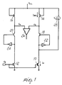
- the reference numerals 10 and 12 respectively indicate a virgin reference cell and a matrix cell of a MOS EPROM memory.
- the sources of two cells 10 and 12 are connected to the ground, and their gates are driven in common by a selection voltage V G .
- the drains of the two cells 10 and 12 are fed by a supply voltage V CC through respective natural load transistors 14, 16 with high gates, arranged in series to respective N-channel transistors 18, 20 the gates whereof are driven by inverters 22, 24, and having the purpose of maintaining, during reading and in a per se known manner, the drains of the cells at such voltage values as to cause no spurious writings.
- the node V R between the transistors 14 and 18, on the reference side, and the node V S between the transistors 16 and 20, on the matrix side are connected to the two inputs of a differential sense amplifier 26.
- a current generator 28 is connected between the power supply V CC and the node V R (i.e. the drain of the reference cell 10) and injects an offset current I L in the reference cell 10.
- the current flowing in the load of the reference cell is thus the difference between the current absorbed by the reference cell 10, which is virgin, and that delivered by the offset generator 28 in a constant manner.
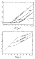
- FIG 2 shows the characteristic curves I V for the virgin cell, I S for the written cell and I ref for the reference cell, as they result from simulation with the ideal circuit arrangement of figure 1, which are shown in figure 2, which also illustrates the behavior of the offset current I L .
- the reference threshold is shifted downward. This is in contrast with what is known from the prior method of current offset, according to which the contribution of current occurred towards the ground on the matrix side: according to the invention the contribution of current is towards the power supply on the reference side.
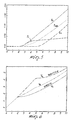
- Figure 3 shows the characteristic curves of the voltages on the output nodes, also obtained by simulation, both for the reference cell (V R ) and for the written and virgin matrix cells (V S ).
- the characteristic curve of the reference current is no longer in an intermediate position between the characteristic curves of the virgin cell and of the written cell when the supply voltage drops below certain limits. This can give rise to spurious readings for very low supply voltages. In order to avoid this condition, it would be desirable to have a constant offset current only starting from a certain value of V CC .
- the offset current generator 28 is constituted as illustrated in figure 4.
- a constant voltage generator V ref is used, formed by two virgin cells 30, 32 with gates connected in common to the drain of the cell 30, and with unbalanced loads.
- the load of the cell 30 comprises two saturated transistors 34, 36 arranged in series, a transistor 38 controlled in negative feedback as described hereafter, and a natural transistor 40, also having a high gate.
- the load of the cell 32 is constituted by a P-channel transistor 42, the gate whereof is also controlled by the drain of the cell 30.
- V ref The output voltage (V ref ) in the node between the drain of the virgin cell 32 and the source of the transistor 42 is given by the sum of the voltage drops between the sources and the gates of the transistors 30, 34, 36 and 38.
- the stability of said voltage is ensured by the negative feedback obtained by applying the same voltage V ref to the gate of the transistor 38.
- the voltage V ref is applied, by means of a further virgin cell 44, to a current mirror 46 the output whereof constitutes the offset current I L .
- Per se known circuits having the purpose of keeping the drain of the cells at such a voltage as to prevent a spurious reading may be connected on the input and output branches of the current mirror 46.
- the creation of the offset current is scarcely influenced by the variations of the manufacturing process.
- the load of the reference side delivers less current than the load of the matrix side, since part of the current required by the cell is provided by the offset. Less current thus always flows across the reference load, and the voltage drop on the node V R (figure 4) is consequently always greater than on the node V S .
- Figure 7 illustrates the dynamic behavior, obtained by simulation, for both a written cell and a virgin cell. It can be seen that there is no time difference between the beginning of the separation of the characteristic curves during a virgin cell reading phase and during a written cell reading phase. The only possible difference may be caused, in the practical case, by the sensitivity of the amplifier stage which follows.
Landscapes
- Read Only Memory (AREA)
- Logic Circuits (AREA)
Applications Claiming Priority (2)
| Application Number | Priority Date | Filing Date | Title |
|---|---|---|---|
| IT19254/88A IT1221780B (it) | 1988-01-29 | 1988-01-29 | Circuito di rilevamento dello stato di celle di matrice in memorie eprom in tecnologia mos |
| IT1925488 | 1988-01-29 |
Publications (3)
| Publication Number | Publication Date |
|---|---|
| EP0326004A2 EP0326004A2 (en) | 1989-08-02 |
| EP0326004A3 EP0326004A3 (en) | 1991-06-12 |
| EP0326004B1 true EP0326004B1 (en) | 1993-10-20 |
Family
ID=11156153
Family Applications (1)
| Application Number | Title | Priority Date | Filing Date |
|---|---|---|---|
| EP89100780A Expired - Lifetime EP0326004B1 (en) | 1988-01-29 | 1989-01-18 | Circuit for sensing the state of matrix cells in MOS EPROM memories |
Country Status (5)
| Country | Link |
|---|---|
| US (1) | US4949307A (it) |
| EP (1) | EP0326004B1 (it) |
| JP (1) | JP2784023B2 (it) |
| DE (1) | DE68909959T2 (it) |
| IT (1) | IT1221780B (it) |
Families Citing this family (15)
| Publication number | Priority date | Publication date | Assignee | Title |
|---|---|---|---|---|
| JPH0793033B2 (ja) * | 1989-08-24 | 1995-10-09 | 日本電気株式会社 | センスアンプ |
| JP2558904B2 (ja) * | 1990-01-19 | 1996-11-27 | 株式会社東芝 | 半導体集積回路 |
| JPH03241594A (ja) * | 1990-02-19 | 1991-10-28 | Fujitsu Ltd | 半導体メモリのセンス回路 |
| IT1246241B (it) * | 1990-02-23 | 1994-11-17 | Sgs Thomson Microelectronics | Circuito per la lettura dell'informazione contenuta in celle di memoria non volatili |
| FR2665792B1 (fr) * | 1990-08-08 | 1993-06-11 | Sgs Thomson Microelectronics | Memoire integree pourvue de moyens de test ameliores. |
| DE69026946T2 (de) * | 1990-11-19 | 1996-09-05 | Sgs Thomson Microelectronics | Verbesserte Abfühlschaltung für Speicheranordnungen wie nichtflüchtige Speicher mit kompensiertem Offsetstrom |
| DE69026828T2 (de) * | 1990-12-13 | 1996-10-02 | Sgs Thomson Microelectronics | Verbesserte Abfühlschaltung für Speicheranordnungen, wie nichtflüchtige Speicher, mit verbesserter Abfühlunterscheidung |
| EP0536095B1 (en) * | 1991-09-26 | 1998-01-21 | STMicroelectronics S.r.l. | Sense amplifier |
| US5487045A (en) * | 1994-09-16 | 1996-01-23 | Philips Electroics North America Corporation | Sense amplifier having variable sensing load for non-volatile memory |
| DE69629668T2 (de) * | 1996-06-18 | 2004-07-08 | Stmicroelectronics S.R.L., Agrate Brianza | Verfahren und Schaltung zum Erzeugen eines Lesereferenzsignals für nichtflüchtige Speicherzellen |
| US5805500A (en) * | 1997-06-18 | 1998-09-08 | Sgs-Thomson Microelectronics S.R.L. | Circuit and method for generating a read reference signal for nonvolatile memory cells |
| US6538922B1 (en) | 2000-09-27 | 2003-03-25 | Sandisk Corporation | Writable tracking cells |
| ITMI20011311A1 (it) * | 2001-06-21 | 2002-12-21 | St Microelectronics Srl | Memoria con sistema di lettura differenziale perfezionato |
| US7237074B2 (en) | 2003-06-13 | 2007-06-26 | Sandisk Corporation | Tracking cells for a memory system |
| US7301807B2 (en) | 2003-10-23 | 2007-11-27 | Sandisk Corporation | Writable tracking cells |
Family Cites Families (4)
| Publication number | Priority date | Publication date | Assignee | Title |
|---|---|---|---|---|
| JPS6173300A (ja) * | 1984-09-17 | 1986-04-15 | Toshiba Corp | 半導体記憶装置 |
| IT1221018B (it) * | 1985-03-28 | 1990-06-21 | Giulio Casagrande | Dispositivo per verificare celle di memoria in funzione del salto di soglia ottenibile in fase di scrittura |
| IT1213343B (it) * | 1986-09-12 | 1989-12-20 | Sgs Microelettronica Spa | Circuito di rilevamento dello stato di celle di matrice in memorie eprom in tecnologia mos. |
| IT1214246B (it) * | 1987-05-27 | 1990-01-10 | Sgs Microelettronica Spa | Dispositivo di memoria non volatile ad elevato numero di cicli di modifica. |
-
1988
- 1988-01-29 IT IT19254/88A patent/IT1221780B/it active
-
1989
- 1989-01-18 DE DE89100780T patent/DE68909959T2/de not_active Expired - Fee Related
- 1989-01-18 EP EP89100780A patent/EP0326004B1/en not_active Expired - Lifetime
- 1989-01-18 US US07/298,487 patent/US4949307A/en not_active Expired - Lifetime
- 1989-01-27 JP JP1937489A patent/JP2784023B2/ja not_active Expired - Fee Related
Also Published As
| Publication number | Publication date |
|---|---|
| DE68909959T2 (de) | 1994-05-05 |
| US4949307A (en) | 1990-08-14 |
| EP0326004A2 (en) | 1989-08-02 |
| IT8819254A0 (it) | 1988-01-29 |
| JP2784023B2 (ja) | 1998-08-06 |
| DE68909959D1 (de) | 1993-11-25 |
| IT1221780B (it) | 1990-07-12 |
| JPH029095A (ja) | 1990-01-12 |
| EP0326004A3 (en) | 1991-06-12 |
Similar Documents
| Publication | Publication Date | Title |
|---|---|---|
| EP0326004B1 (en) | Circuit for sensing the state of matrix cells in MOS EPROM memories | |
| US5805500A (en) | Circuit and method for generating a read reference signal for nonvolatile memory cells | |
| US5638332A (en) | Integrated circuit memory device with balancing circuit including follower amplifier coupled to bit line | |
| US5493533A (en) | Dual differential trans-impedance sense amplifier and method | |
| KR0122108B1 (ko) | 반도체 메모리 장치의 비트라인 센싱회로 및 그 방법 | |
| US5390147A (en) | Core organization and sense amplifier having lubricating current, active clamping and buffered sense node for speed enhancement for non-volatile memory | |
| KR930001735B1 (ko) | 반도체 기억장치 | |
| US5886925A (en) | Read circuit and method for nonvolatile memory cells with an equalizing structure | |
| EP0729633B1 (en) | Sense amplifier for non-volatile semiconductor memory | |
| US5572465A (en) | Power supply configured sensing scheme for flash EEPROM | |
| US5250854A (en) | Bitline pull-up circuit operable in a low-resistance test mode | |
| US5663915A (en) | Amplifier and method for sensing having a pre-bias or coupling step | |
| US4542485A (en) | Semiconductor integrated circuit | |
| US4611301A (en) | Read only memory | |
| US5369614A (en) | Detecting amplifier with current mirror structure | |
| JPS61117915A (ja) | 遅延回路 | |
| IE50902B1 (en) | Circuit for maintaining the potential of a node of an mos dynamic circuit | |
| US5027320A (en) | EPROM circuit having enhanced programmability and improved speed and reliability | |
| EP0270750B1 (en) | Sense circuit for the state of matrix cells in mos eprom memories | |
| US4464591A (en) | Current difference sense amplifier | |
| JPH0323997B2 (it) | ||
| JP3184984B2 (ja) | 書き込まれているセルの書き込まれていないセルに対するしきい値のジャンプから独立した動作フィールドを有するepromメモリセルのための読み出し装置 | |
| JPH05225792A (ja) | Nand型セルを具備したメモリ装置の感知装置 | |
| KR930008413B1 (ko) | 반도체기억장치 | |
| US5864507A (en) | Dual level wordline clamp for reduced memory cell current |
Legal Events
| Date | Code | Title | Description |
|---|---|---|---|
| PUAI | Public reference made under article 153(3) epc to a published international application that has entered the european phase |
Free format text: ORIGINAL CODE: 0009012 |
|
| AK | Designated contracting states |
Kind code of ref document: A2 Designated state(s): DE FR GB NL SE |
|
| PUAL | Search report despatched |
Free format text: ORIGINAL CODE: 0009013 |
|
| AK | Designated contracting states |
Kind code of ref document: A3 Designated state(s): DE FR GB NL SE |
|
| 17P | Request for examination filed |
Effective date: 19910902 |
|
| 17Q | First examination report despatched |
Effective date: 19930322 |
|
| GRAA | (expected) grant |
Free format text: ORIGINAL CODE: 0009210 |
|
| AK | Designated contracting states |
Kind code of ref document: B1 Designated state(s): DE FR GB NL SE |
|
| REF | Corresponds to: |
Ref document number: 68909959 Country of ref document: DE Date of ref document: 19931125 |
|
| ET | Fr: translation filed | ||
| PLBE | No opposition filed within time limit |
Free format text: ORIGINAL CODE: 0009261 |
|
| STAA | Information on the status of an ep patent application or granted ep patent |
Free format text: STATUS: NO OPPOSITION FILED WITHIN TIME LIMIT |
|
| 26N | No opposition filed | ||
| EAL | Se: european patent in force in sweden |
Ref document number: 89100780.9 |
|
| REG | Reference to a national code |
Ref country code: FR Ref legal event code: D6 |
|
| PGFP | Annual fee paid to national office [announced via postgrant information from national office to epo] |
Ref country code: SE Payment date: 20010105 Year of fee payment: 13 |
|
| PGFP | Annual fee paid to national office [announced via postgrant information from national office to epo] |
Ref country code: DE Payment date: 20010108 Year of fee payment: 13 |
|
| PGFP | Annual fee paid to national office [announced via postgrant information from national office to epo] |
Ref country code: GB Payment date: 20010118 Year of fee payment: 13 |
|
| PGFP | Annual fee paid to national office [announced via postgrant information from national office to epo] |
Ref country code: FR Payment date: 20010125 Year of fee payment: 13 |
|
| PGFP | Annual fee paid to national office [announced via postgrant information from national office to epo] |
Ref country code: NL Payment date: 20010131 Year of fee payment: 13 |
|
| REG | Reference to a national code |
Ref country code: GB Ref legal event code: IF02 |
|
| PG25 | Lapsed in a contracting state [announced via postgrant information from national office to epo] |
Ref country code: GB Free format text: LAPSE BECAUSE OF NON-PAYMENT OF DUE FEES Effective date: 20020118 |
|
| PG25 | Lapsed in a contracting state [announced via postgrant information from national office to epo] |
Ref country code: SE Free format text: LAPSE BECAUSE OF NON-PAYMENT OF DUE FEES Effective date: 20020119 |
|
| PG25 | Lapsed in a contracting state [announced via postgrant information from national office to epo] |
Ref country code: NL Free format text: LAPSE BECAUSE OF NON-PAYMENT OF DUE FEES Effective date: 20020801 Ref country code: DE Free format text: LAPSE BECAUSE OF NON-PAYMENT OF DUE FEES Effective date: 20020801 |
|
| EUG | Se: european patent has lapsed |
Ref document number: 89100780.9 |
|
| GBPC | Gb: european patent ceased through non-payment of renewal fee |
Effective date: 20020118 |
|
| PG25 | Lapsed in a contracting state [announced via postgrant information from national office to epo] |
Ref country code: FR Free format text: LAPSE BECAUSE OF NON-PAYMENT OF DUE FEES Effective date: 20020930 |
|
| NLV4 | Nl: lapsed or anulled due to non-payment of the annual fee |
Effective date: 20020801 |
|
| REG | Reference to a national code |
Ref country code: FR Ref legal event code: ST |