EP0325077B1 - Abtasterschnittstelle für Leitungsadapter einer Übertragungssteuerung - Google Patents
Abtasterschnittstelle für Leitungsadapter einer Übertragungssteuerung Download PDFInfo
- Publication number
- EP0325077B1 EP0325077B1 EP88480001A EP88480001A EP0325077B1 EP 0325077 B1 EP0325077 B1 EP 0325077B1 EP 88480001 A EP88480001 A EP 88480001A EP 88480001 A EP88480001 A EP 88480001A EP 0325077 B1 EP0325077 B1 EP 0325077B1
- Authority
- EP
- European Patent Office
- Prior art keywords
- data
- line
- fes
- control
- serial link
- Prior art date
- Legal status (The legal status is an assumption and is not a legal conclusion. Google has not performed a legal analysis and makes no representation as to the accuracy of the status listed.)
- Expired - Lifetime
Links
Images


Classifications
-
- G—PHYSICS
- G06—COMPUTING OR CALCULATING; COUNTING
- G06F—ELECTRIC DIGITAL DATA PROCESSING
- G06F13/00—Interconnection of, or transfer of information or other signals between, memories, input/output devices or central processing units
- G06F13/14—Handling requests for interconnection or transfer
- G06F13/20—Handling requests for interconnection or transfer for access to input/output bus
- G06F13/22—Handling requests for interconnection or transfer for access to input/output bus using successive scanning, e.g. polling
- G06F13/225—Handling requests for interconnection or transfer for access to input/output bus using successive scanning, e.g. polling with priority control
-
- G—PHYSICS
- G06—COMPUTING OR CALCULATING; COUNTING
- G06F—ELECTRIC DIGITAL DATA PROCESSING
- G06F13/00—Interconnection of, or transfer of information or other signals between, memories, input/output devices or central processing units
- G06F13/38—Information transfer, e.g. on bus
- G06F13/382—Information transfer, e.g. on bus using universal interface adapter
- G06F13/385—Information transfer, e.g. on bus using universal interface adapter for adaptation of a particular data processing system to different peripheral devices
Definitions
- the present invention relates to the line adapters of a communication device, especially a communication controller.
- Communications controllers are used for managing the transmissions within a teleprocessing environment, to which a plurality of users terminals are connected through transmission lines.
- the main objective of line adapters is to allow groups of transmission lines to exchange information with the Central Control Unit (CCU) of the communication controller, thus avoiding to connect each line individually to said CCU. Therefore, the line adapters include scanning means, for cyclically scanning the lines.
- CCU Central Control Unit
- the line adapters include scanning means, for cyclically scanning the lines.
- Such aline adapter has already been described in Patent Applications EP-A-0,048,781 and EP-077,863.
- the transmission lines connected to the users terminals exchange information with the scanning means through line interface circuits (LICs) regrouped on a LIC unit.
- Each LIC unit can include up to eight LICs and is connected to the scanning means by a parallel bus and adequate connectors, which have quite a large size and are accordingly space consuming in the machine, and expensive.
- the LIC units and multiplexer interfaces can be, if necessary, implemented outside of the Communications Controller machine frame or at it's periphery, and accordingly, the connectivity, LIC switchability and overall performances are increased.
- US patent A - 4 296 464 is related to an interface control unit for a computer control system which interfaces between a parallel communication bus and a serial communication bus. This interface does not solve the asynchronism problem which is raised in the subject environment wherein the FES and the serial link work with asynchronous timings.
- FES Front End Scanner Adapter
- the FES is the master device and the FESA has to take the information presented by the FES immediately. Similarly, when the FES requires information from a given line X, the FESA must have this information ready for it.
- the line adapter (1) is provided in a communications controller, for exchanging data and control information between line interface circuits LIC's (20) connected to external transmission lines (26) and the central control unit (CCU) of the communications controller. It includes for scanning the lines (26), cyclic scanning means FES (10) exchanging information with the line interface circuits through a bidirectional serial link (12) comprising an inbound serial link ISL (24) and an outbound serial link (OSL) on which data and control information are partitioned into frames comprised of data slots and control slots, each couple of data and control slots being dedicated to a predetermined line (26).
- a bidirectional serial link (12) comprising an inbound serial link ISL (24) and an outbound serial link (OSL) on which data and control information are partitioned into frames comprised of data slots and control slots, each couple of data and control slots being dedicated to a predetermined line (26).
- the line adapter (1) is characterized by the fact that the scanning means FES (10) and serial link (12) being operated independently according to their own timings, it includes a front end scanner adapter interface FESA (11), for interfacing said cyclic scanning means FES (10) with said bidirectional serial link (12).
- FESA front end scanner adapter interface
- the front end scanner adapter interface comprises : storage means (36, 38, 40, 42) for storing, on the one hand, data and control information transmitted from the line interface circuits LIC's (20) to the cyclic scanning means FES through the inbound serial link ISL (24) and on the other hand, data and control information transmitted from the cyclic scanning means FES (10) to the line interface circuits LIC's (20) through the outbound serial link (22) first interfacing means (66,68,70,72,73) attached to the cyclic scanning means FES (10) for allowing said cyclic scanning to process the information stored in the storage means during timing steps generated by a first step counting means (162) at each line scan period, second interfacing means (56,60,61) attached to the inbound serial link ISL (24) for processing the information received therefrom and load it into the storage means during timing steps generated by a second step counting means ( 110) at each line process period, third interfacing means (62,63,58) attached to the outbound serial link OSL (22) for fetching the information
- Figure 1 represents a schematic block diagram of a system wherein the invention may be used.
- Figure 2 represents schematically the transmission subsystem of a communication device, incorporating the FESA interface according to the invention.
- FIG. 3 represents schematically the information exchanges between FES and Serial Link.
- Figure 4 represents the structure of the Serial Link information flow.
- Figure 5 represents a schematic block diagram of the FESA interface.
- Figure 6 represents the structure of the FESA for data transmitted from the serial link to the FES.
- Figure 7 represents the structure of the interface of the FESA with the serial link.
- Figure 8 represents the steps of the inbound serial link data process.
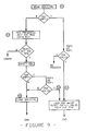
- Figure 9 represents the operations needed for transmitting data from the FES to the FESA.
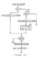
- Figure 10 represents the operations needed for transmitting data from the FESA to the FES.
- Figure 11 represents the structure of the FESA for data transmitted from the FES to the serial link.
- Figure 12 represents a logic circuit for detecting full data slots.
- Figure 13 represents the structure of the FESA for transmitting control information between the FES and the serial link.
- Figure 14 represents an arbitration circuit giving selective access to the data RAMS.
- FIG. 1 illustrates a global scheme of a system which can use this invention.
- Communication Controller CC is an element of a teleprocessing network of a type disclosed in the book "Tele- disposition", by G. Macchi and J.E. Guilbert, 1979, published by Dunod, more specifically, under Chapter 10.
- a central control unit CCU handles the data transmitted between terminals T and central processing units CPU1 and CPU2.
- Unit CCU is connected to multiplex channel (MPX) buses for the central processing units CPU1 and CPU2 via channel adapters CA1, ...CAn. It is also coupled to terminals T via line adapters LA1, ..., LAn connected to a CCU bus.
- MPX multiplex channel
- FIG 2 is a schematic diagram of a line adapter (1) as referenced by LA in Figure 1.
- a line adapter (1) is comprised of a microprocessor (16) running the microcode contained in a microcode memory (17), and of a scanning logic (10) designated by FES (10) (Front End Scanner) in the Figure, about which more details are available in European Patent No. EP-A-0,048,781 related to a communication line adapter for a communications controller.
- the data exchange between the LICs (20) and the scanning means will preferably be done through a multiplexing circuit (14) and a serial link (12) as further described.
- the line adapter includes a Front End Scanner Adapter FESA (11) for adapting the parallel interface of the FES (10) to the serial link architecture as further described with reference to Figure 5.
- the FESA (11) must be transparent to the FES. This means that the FES (10) performs its scanning operations as it did when it was connected to the LICs by a parallel bus, as described in patent applications EP-A-0,048,781 and EP-A-077,863.
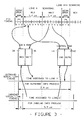
- the scanning timing of the FES is briefly remembered in Figure 3 : the scanning of a given line X includes a receive phase and a transmit phase, each of which comprise seven steps (0 to 6) provided by a sequencing logic (not shown). When the scanning of line X is finished, it is normally followed by the scanning of line (X+4).
- the synchronous scanning protocol of the FES can be interrupted, at the end of line scanning, by an asynchronous operation of the microcode, the latter wanting immediate read or write access to a LIC register.
- Figure 3 gives an idea of the problem of asynchronism to solve by the invention. While the FES performs the scanning of line X, the outbound serial link (OSL) works on information to be transmitted to a line Y, and the inbound serial link (ISL) works on information received from a line Z.
- OSL outbound serial link
- ISL inbound serial link
- the main problem to be solved by the FESA (11) is the problem of asynchronism between several components connected to it, and which need to be able to exchange information. Since, it is implemented between the FES (10) and the serial link (12) of the line-adapter (1), the FESA has to meet the requirements of four independent users : the FES hardware, the FES microcode, the outbound serial link, and the inbound serial link. Therefore, as will be further described, the FESA will include storage means between the FES (10) and the serial link (12), said storage means being preferably embodied by data RAMs (36, 38) and control RAMs (40, 42) as shown in Figure 5. In same figure, the different arrows show the possible information flows between the slots of the serial link and the RAMs, and the possible information flows between the RAMs and the FES. These information flows require the implementation of interfacing logic further described.
- the FESA design must not impact the FES performance.
- the FESA must handle the FES and microcode requests (which will be briefly recalled further) as they are in the IBM 3725 design, which means that these requests are served with the highest priority by the FESA, while the outbound and inbound requests of the serial link receive a lower priority.
- FIG. 2 shows that the FES/FESA is connected, for instance, to eight Line Interface circuits (LICs) (20) through a serial link (12) and a multiplexor (14).
- LICs Line Interface circuits
- Each LIC supports up to four serial transmission lines (26) connected to a user terminal (28), eventually through modems (30).
- each line adapter includes a scanning device, performing the scanning of the lines according to a certain sequential scanning scheme : in synchronous operation mode, the time interval between two line scans must be shorter than the time interval between two bits which are transmitted or received.
- the maximum scanning speed of the device of the invention is 350 000 received or emitted bits per second (transmission through four wires also called "full duplex" transmission). This scanning power is automatically distributed amongst the number of connected lines. If there is one line, it would be able to operate at 256 000 bits per second.
- each LIC circuit can be connected to one or four lines. It is possible to have one to eight LIC circuits, each one being provided on a so-called LIC card and connected to a scanning device. The number of the LIC circuits which are connected, automatically modifies the line scanning. When eight LIC circuits are installed in the 0 to 7 order, the line scanning is always performed in the following order, by the FES as described in said patent applications.
- the FESA could easily be adapted to a FES having another scanning scheme.
- the FESA includes interfacing logic (68, 70, 72) with the FES, as will be further described in relation to Figure 5. But, it has to be noted that, since the FES (10) is not affected by the presence of the FESA, it presents the normal interfacing wires, as described in patent EP-A-0,077,863, the most important of which are hereunder recalled :
- ASYNC OPERATION is a new timing tag. It signals asynchronous microcode operations on the FESA or on the line frame components.
- the FESA according to the invention also provides interfacing means (60, 61, 62, 63) with the serial link (12).
- interfacing means 60, 61, 62, 63
- serial link architecture in relation to Figure 4.
- a given FRAME transfers the same kind of control information for all the 32 equipments.
- Figure 4c shows the FRAME assignation in the present specification, where a centralized scanner controls 32 teleprocessing lines : in this SUPERFRAME organization, all frames are devoted to a determined control register of one of the LIC, multiplexor or line registers, being understood that the 32 line interface equipments are implemented in 8 Line interface couplers (LIC's) of 4 lines each.
- LIC's Line interface couplers
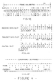
- Data Burst do not depend on the frame number, and are represented in Figure 4a. Depending on the data traffic, the data burst can vary from 0 to 5 bits.
- the control slot format is the same in both ways :
- the control information is set in bits 1 to 6.
- Bit 0 is set to '1' in all control slots of FRAME 31 to allow the two ends of the serial link to check and keep the superframe synchronization.
- bits are encoded according to the differential Manchester code.
- a specific code violation pattern is sent at each end of frame by each sending part to allow the opposite receiving part to detect the beginning of next fram.
- the frame duration is 125 microseconds and a superframe lasts 4 milliseconds.
- the data and control slots taken from the inbound serial link (12) are transmitted by bursts to the inbound serial link interface (56), then processed according to the steps provided by a process logic (60, 61).
- the data are put in appropriate form for storage in a "Receive Data RAM” (38), where they are kept ready for a bit after bit scanning by the FES through a data bit interface (70).
- control data slots provided by the inbound serial link are similarly put in appropriate form for storage in an "Inbound Control RAM” (40), while some specific control registers (LIC present, LIC wideband) directly needed by the FES or microcode are transmitted directly through line (71), to a scan control logic (72), described in relation to Figure 13.
- LIC Inbound Control RAM
- the control information to be transmitted to the LICs through the OSL is ready for outbound transmission, performed by the outbound control process logic (63) and OSL interface (58).
- the control process logic (63) is in charge of fetching the control words from the outbound control RAM, and therefore provides necessary timing signals.
- arbitration means (100) are provided. They do not appear on Figure 5, but will be described in Figure 14.
- Figure 5 further shows a FESA control register unit (66), which exchanges control informations with the FES control bus (80) through the control interface (68).
- a variety of control registers can be included into the unit (66) : error reporting registers, FESA diagnostics registers etc.., but they are not really part of the present invention.
- control register unit mainly contains a FESA control register, each bit of which is used for controlling a specific operation mode of the FESA.
- the possible operation modes of the FESA are indicated below.
- the FESA can be under reset, in "reset RAMs” state, in Freeze state, or in "free-running” mode, which allows the FESA normal operation.
- Reset FESA is a control lead coming from the FES, active during the FES reset (cf FES/FESA interface).
- this command resets all the logic (reset latches, including the control Reg bit 0), but sets the control Reg bit 1 (reset RAMs), in order to initialize the reset of the FESA RAMs when reset FESA becomes inactive at the interface.
- This reset is activated by microcode, by setting the FESA control Reg bit 0.
- This command has the same characteristics as reset FESA, except that :
- Next state can be "reset RAMs”, “Freeze”, or “free-running”, depending on the bits set or not by microcode in the control Reg, at the time it removed reset latches.
- the FESA reset RAMs can be started :
- the operation resets all FESA RAMs.
- control Reg bit 1 is set automatically
- freeze mode if the control Reg bit 2 (Freeze) has been set by the microcode at the time it reset bit 0.
- the FESA RAMs can be loaded or dumped.
- Freeze is fully controlled by microcode, by setting and resetting the control Reg bit 2.
- the microcode To pass to the free-running state, the microcode must reset freeze. However, the free-running state will be correct (serial link synchronized) only if the following sequences are respected :
- control RAMs address extension bit Two further bits (3, 4) are provided, respectively called “control RAMs address extension bit” and “control RAMs swap” bit, described farther.
- Figure 6 shows the structure of the FESA hardware for inbound data transmission, i.e. data transmitted from ISL line (24) to the FES (10), through inbound serial link interface (56), inbound data process logic (60), receive data RAM (38) and receive data bit interface (70).
- the data RAMs (36, 38) contain, for each line, receive (RCV) and transmit (Xmit) data buffers plus a set of control bits.
- the FESA receives data bursts from the lines through the Inbound S.L. data slots (shown in Figure 4) and serializes the data, to feed the FES bit by bit.
- the data RCV RAM (38) needs 32 areas (LO to L31) of 4 bytes each, a RCV SDF byte (74), a RCV SDF CTRL byte (76), a RCV PDFO byte (78) and a RCV PDF1 byte (82), where SDF stands for "Serial Data Field” and PDF stands for "Parallel Data Field”.
- the cited RAM fields are working areas for the FESA, to assemble or serialize the data bursts, in a way described hereunder.
- Each LIC fills its assigned Data Slots with the data available at the time the Inbound S.L. scans its line(s).
- the RCV data burst length depends upon the line speed. It can vary from 0 to 5 bits with the serial link used in the present invention. However, a similar serial link using bursts of constant length could work with the FESA provided by the invention.
- the inbound S.L. data slots are processed by the FESA in the following way :
- the table shows an example of content of the bytes (74, 76, 78, 82) content, where Ri designs a received bit number i.
- the bit 0 of byte SDF CTL (76), called PDF0 valid means, when set to "1", that the PDF0 has been set with a data burst coming from the Inbound Serial Link.
- the ISL must monitor the PDF0 valid bit and the PDF1 valid bit in order to determine which PDF field should be loaded with a new data burst. This is done by an update logic (88) as described below.
- PDF1 has a similar meaning.
- PDF PTR pointer
- FIG 8 shows a summ-up of the operations performed by the ISL data process logic (60), according to several ISL steps (ISL S0 to S3) generated by an ISL timing steps generator (110), as described farther ( Figure 7).
- the address of the RCV data RAM (38) where the processed data burst has to be written, upon activation of WR command, is specified by an address bus (81) containing the slot and frame address of the considered line in the serial link.
- This address is generated by an address decoder (108) shown in Figure 7, and receiving its clocking from an ISL counter (118), which provides the slot and frame counts of the serial link.
- the data bursts are ready for transmission to the FES (10), bit after bit, through the data bit receive interface (70).
- the SDF (74) and SDF CTRL (76) are loaded respectively into a SDF shift register (84) and a SDF CTRL register (86) both implemented in the data bit receive interface (70).
- Figure 9 shows a summ-up of the operations performed when a SDF (74) stored in the data RAM (38) is to be transmitted bit by bit to the FES.
- FIG. 7 shows the structure of the inbound/outbound serial link interfaces (56, 58).
- the Manchester encoded information from the ISL line (24) is received through a receiver circuit (126) and buffered to a Manchester decoder (116).
- a Manchester decoder 116
- the decoder (116) provides 8-bits information slots to an ISL shift register (106), and at each slot, a counting pulse is provided to the ISL counters (118) wherein slot and frame counts are generated.
- the decodes provided by the address decoder (108) will be used for addressing the inbound control RAM (40) and the data receive RAM (38) (bus (79)).
- the first 8-bits slot provided to the ISL shift register (106) is a data slot, and the next one is a control slot, and so on (cf Figure 4).
- the data and control slots are respectively transmitted by the ISL shift register (106) to an ISL data PDF parallel register (94) and to an ISL CTRL buffer (96), the discrimination being made upon an eight bits count.
- this processing of the slots may not be compulsory if another format is chosen on the serial link.
- the structure of the outbound serial link interface (58) is similar to the inbound one, being understood that the information slots (data/CTRL) are to be transmitted from the outbound data and CTRL RAMs (36, 42) to the OSL.
- the data slots taken from the data Xmit RAM (36) are in the form as provided by the FES, and are accordingly processed (shifted) within the outbound data process logic (62) (mainly a shift register), in order to be loaded into the parallel register constituting the OSL PDF (90).
- outbound data process logic (62) mainly a shift register
- control information is read from the outbound control RAM and loaded into an OSL CTRL buffer (92) through an outbound control process logic (63) which may be facultative, depending on the format of the control slots as stored in the CTRL RAM.
- the data and control slots are transmitted alternatively to an OSL shift register (104) and accordingly serialized into a Manchester encoder (114), and put onto the OSL line (22) through a driver (124).
- OSL slot and frame counters (112) are implemented.
- the slot/frame counts are used by an address decoder (102) which has to feed the Xmit data RAM (36) with the slot and frame addresses ( Figure 11, bus 81), and by an OSL timing steps generator (98).
- Figure 11 shows the global structure of the FESA hardware for outbound data transmission, i.e data transmitted from the FES (10) to the OSL line (22), through a data bit Xmit interface (73), a Xmit data RAM (36), the outbound data process logic (62) and outbound serial link interface (58) as previously described.
- the Xmit data RAM (36) contains, for each of the 32 lines, a SDF byte (130) and its related SDF CTRL byte (132), a PDF (134) byte and its related control byte PDF CTRL (136).
- the transmit data bit is assembled in the transmit SDF field (138).
- a simple circuit included in interface (73) is provided, as shown in Figure 12, for detecting a full SDF, according to the burst size allowed for the line being scanned.
- PDF TAKEN is a working bit which is set by the outbound S.L. process when the PDF is sent to the LIC. It means that the waiting SDF (130) can be loaded in the PDF field (134).
- PDF TAKEN is reset by the FESA after the transfer of SDF to PDF.
- control RAM is made of 2 parts : the outbound control RAM (42), which bufferizes the control information in the outbound way, and the inbound control RAM (40) which bufferizes the information in the inbound way, for the 32 lines as well.
- the stored control information comprises control registers for the MUX (14), the LIC registers of the 32 lines, plus 32 sets (one set per line) of work registers managed by the FESA to process the lines.
- the FES and microcode control information to MUX and LIC's (MUX and LIC's write registers) is stored in the outbound control RAM (42) and wait for the proper slots of the outgoing frames to be sent on the outbound serial link.
- the MUX and LIC registers information entering the FESA on the inbound serial link is stored in the inbound control RAM (40), and waits for the FES and microcode requests.
- Figure 13 shows the FESA organization for the exchange of control registers between the FES (10) and the LICs.
- the MUX, LIC or line control slots provided by the ISL control buffer (96) of the ISL interface (56) ( Figure 7) are loaded into the inbound control RAM (40) through an inbound control process logic (61).
- the ISL RAM addressing bus (160) is provided by the slot-frame address decoder (108) as explained in relation to Figure 7.
- the inbound control process logic (61) includes an ISL step counter (170) ( Figure 14) which delivers four steps ISL S0 to S3.
- Step S0 the content of the current control slot is loaded into the inbound CTL RAM (40).
- Steps S1 to S3 are used to update the scan control registers (72) as previously mentioned ( Figure 5).
- a first register "LIC present register” is updated during frame 13, on reception of the line control register.
- a second register “LIC wideband” is updated during frame 7, on reception of the LIC type information, telling if a given LIC is wideband (a wideband line is scanned four times more often than a not wideband line).
- the control interface (68) is in charge of fetching from the inbound CTL RAM (40), the control information needed by the FES or the microcode to control the lines.
- step S1 of the FES RCV timing the FES inputs from the inbound CTRL RAM (40) the control information relative to the attached modem.
- step S6 of the FES transmit timing the FES provides control information to the modem. This information is thus loaded into the outbound control RAM (42) on step S6 of FES transmit timing.
- Interface (68) mainly includes a register (buffer), and gating logic. It is also used by the microcode, either to write control information in the outbound control RAM (42) or to read control information from the inbound control RAM (40).
- the RAM address can have 2 different (but equivalent) forms :
- the RAMS SWAP bit (bit 4 of register (66) can be set by microcode, to allow a full RD/WR access to the FESA control RAMS, according to the following table :
- the RAMs are time-shared by the FES and the 2 serial link interfaces (inbound and outbound).
- the FESA has to synchronize the various RAM requests and to arbitrate them :
- the remaining time is available for the 2 serial link interfaces. This time is shared as follows :
- the RAM access arbitration problem is solved by an arbitration logic (100) shown in Figure 14, for the case of a control information process, being understood that a very similar circuit is implemented for the case of data process.
- the Figure 14 shows the three counters (162, 166, 170) which generate the steps necessary to access the control RAM by the different RAM users : FES, OSL, ISL.
- S1R means : step S1 of the FES receive timing.
- the FES step counter (162) is triggered by the receive/transmit signal of the FES interface, the OSL step counter is triggered by the occurence of OSL data bit 0 time giving the beginning of the OSL data process.
- the ISL step counter is triggered by ISL data bit 0 time.
- the FES timing has the highest priority. Thus, there is no hold condition on step counter (162).
- OSL step counter (166) is held by the FES steps through OR gate (164), while the ISL step counter is held by OR gate (168) obtained by combining the output of OR gate (164) and OSL step S0.
- OSL and ISL step counters are held in the same way, except that OSL step counter is additionally held by the transmit timing of the FES, and ISL by the receive timing of the FES.
Landscapes
- Engineering & Computer Science (AREA)
- Theoretical Computer Science (AREA)
- Physics & Mathematics (AREA)
- General Engineering & Computer Science (AREA)
- General Physics & Mathematics (AREA)
- Communication Control (AREA)
- Small-Scale Networks (AREA)
- Data Exchanges In Wide-Area Networks (AREA)
Claims (5)
- Leitungsadapter (1) einer Übertragungssteuereinheit zum Austauschen von Daten- und Steuerungsinformationen zwischen Schnittstellenschaltungen für Leitungen LIC's (20), die mit externen Übertragungsleitungen (26) verbunden sind und der zentralen Steuereinheit (CCU) der Übertragungssteuereinheit, wobei der Leitungsadapter zum Abfragen der Leitungen (26) ein Mittel zum zyklischen Abfragen, FES (10) aufweist, das mit den Schnittstellenschaltungen für Leitungen über eine zweiseitig gerichtete serielle Verbindung (12) Informationen austauscht, die eine einlaufende serielle Verbindung, ISL (24) und eine auslaufende serielle Verbindung, OSL (22) aufweist, auf welchen Daten- und Steuerungsinformationen in Rahmen geteilt werden, die Datenschlitze und Steuerungsschlitze aufweisen, wobei jedes Paar von Daten- und Steuerungsschlitzen einer vorbestimmten Leitung (26) zugeordnet ist, und der Leitungsadapter (1) dadurch gekennzeichnet ist, daß das Mittel zum Abfragen, FES (10) und die serielle Verbindung (12) unabhängig, entsprechend ihren eigenen Zeitgebungen betrieben werden, wobei er eine Schnittstelle für Eingangsabfrageadapter, FESA (11) aufweist, um für das Mittel zum zyklischen Abfragen, FES (10) eine Schnittstelle mit der zweiseitig gerichteten seriellen Verbindung (12) zu bilden, wobei die Schnittstelle für Eingangsabfrageadapter folgendes aufweist:
Speichermittel (36, 38, 40, 42), um folgendes zu speichern: einerseits Daten- und Steuerungsinformationen, die aus den Schnittstellenschaltungen für Leitungen, LIC's (20) über die einlaufende serielle Verbindung, ISL (24) zu dem Mittel zum zyklischen Abfragen, FES übertragen werden und andererseits Daten- und Steuerungsinformationen, die aus dem Mittel zum zyklischen Abfragen, FES (10) über die auslaufende serielle Verbindung (22) zu den Schnittstellenschaltungen für Leitungen, LIC's (20) übertragen werden,
erste Schnittstellenmittel (66, 68, 70, 72, 73), die mit den Mitteln zum zyklischen Abfragen, FES (10) verbunden sind, um es zu ermöglichen, daß das Mittel zum zyklischen Abfragen, FES die Informationen verarbeitet, die während der Taktgeberschritte in den Speichermitteln gespeichert sind, die mittels eines ersten Schrittzählermittels (162) bei jeder Leitungsabtastperiode erzeugt werden,
zweite Schnittstellenmittel (56, 60, 61), die mit der einlaufenden seriellen Verbindung ISL (24) verbunden sind, um die aus dieser empfangenen Informationen zu verarbeiten und sie während Taktgeberschritten in die Speichermittel zu laden, die mittels eines zweiten Schrittzählermittels (110) bei jeder Leitungsverarbeitungsperiode erzeugt werden,
dritte Schnittstellenmittel (62, 63, 58), die mit der auslaufenden seriellen Verbindung OSL (22) verbunden sind, um die Informationen für die auslaufende serielle Verbindung aus den Speichermitteln zu holen und sie während Taktgeberschritten zu verarbeiten, die mittels eines dritten Schrittzählermittels (98) bei jeder Leitungsverarbeitungsperiode erzeugt werden,
ein Entscheidungsmittel (100), um die Prioritäten des Zugriffs auf die Speichermittel mittels der ersten, der zweiten und der dritten Schnittstellenmittel zu bestimmen, wobei die Prioritäten von dem aktuellen Schritt des ersten, des zweiten oder des dritten Zählers auf eine solche Weise abhängen, daß das Entscheidungsmittel die Ausführung des Ablaufs des Schrittes ermöglicht, welcher die höchste Priorität besitzt und gleichzeitig die zwei anderen Schrittzählermittel anhält. - Leitungsadapter nach Anspruch 1, bei welchem die Speichermittel (36, 38, 40, 42) einen Datenempfangsspeicher RAM (38) aufweisen, in welchen die jeder Leitung (26) entsprechenden Datenschlitze unter Steuerung von den zweiten Schnittstellenmitteln in zugeordnete Datenfelder (78, 82) geladen werden, wobei auf den Datenempfangsspeicher bzw. dieser mittels der ersten Schnittstellenmittel zugegriffen bzw. gelesen wird, um den Datenschlitzinhalt Bit für Bit, synchron mit der Empfangsabfragezeitgebung des Mittels zum zyklischen Abfragen, FES (10) zu den Mitteln zum zyklischen Abfragen, FES zu übertragen.
- Leitungsadapter nach Anspruch 2, bei welchem die Speichermittel (36, 38, 40, 42) einen Datenübertragungsspeicher RAM (36) aufweisen, in welchem die jeder Leitung (26) entsprechenden Daten, die Bit für Bit aus dem Mittel zum zyklischen Abfragen, FES (10) entsprechend seiner eigenen Abfragezeitgebung für eine Übertragung übertragen werden und die mittels der ersten Schnittstellenmittel in Datenanhäufungen gesammelt werden, unter Steuerung von den ersten Schnittstellenmitteln geladen werden, wobei auf den Datenübertragungsspeicher von den dritten Schnittstellenmitteln zugegriffen wird, um die Datenanhäufungen jeder Leitung zu lesen und sie auf die auslaufende serielle Verbindung OSL (22) zu übertragen.
- Leitungsadapter nach Anspruch 2 oder 3, bei welchem die Speichermittel (36, 38, 40, 42) einen einlaufenden Steuerungsspeicher RAM (40) aufweisen, in welchen die jeder Leitung (26) entsprechenden Steuerungsschlitze unter Steuerung von den zweiten Schnittstellenmitteln in zugeordnete Steuerungsfelder geladen werden, wobei auf den einlaufenden Steuerungsspeicher bzw. dieser mittels der ersten Schnittstellenmittel zugegriffen bzw. gelesen wird, um den Steuerungsschlitzinhalt auf einem Steuerungsbus (80) zu dem Mittel zum zyklischen Abfragen FES zu übertragen.
- Leitungsadapter nach irgend einem der Ansprüche 2 bis 4, bei welchem die Speichermittel (36, 38, 40, 42) einen auslaufenden Steuerungsspeicher RAM (42) aufweisen, in welchen der jeder Leitung (26) entsprechende Steuerungsschlitzinhalt, der mittels des Mittels (10) zum zyklischen Abfragen, FES (10) über die ersten Schnittstellenmittel übertragen wird, unter Steuerung von den ersten Schnittstellenmitteln in einen Bereich des auslaufenden Steuerungsspeichers RAM (42) geladen wird, welcher der Leitung zugeordnet ist, wobei auf den Datenübertragungsspeicher von den dritten Schnittstellenmitteln zugegriffen wird, um den Steuerungsschlitzinhalt jeder Leitung zu lesen und ihn auf die auslaufende serielle Verbindung OSL (22) zu übertragen.
Priority Applications (5)
| Application Number | Priority Date | Filing Date | Title |
|---|---|---|---|
| DE8888480001T DE3874517T2 (de) | 1988-01-22 | 1988-01-22 | Abtasterschnittstelle fuer leitungsadapter einer uebertragungssteuerung. |
| EP88480001A EP0325077B1 (de) | 1988-01-22 | 1988-01-22 | Abtasterschnittstelle für Leitungsadapter einer Übertragungssteuerung |
| CA000569054A CA1301275C (en) | 1988-01-22 | 1988-06-09 | Scanner interface for the line adapters of a communication controller |
| JP63290375A JPH0624382B2 (ja) | 1988-01-22 | 1988-11-18 | ラインアダプタ |
| US07/297,730 US5010548A (en) | 1988-01-22 | 1989-01-17 | Scanner interface for the line adapters of a communication controller |
Applications Claiming Priority (1)
| Application Number | Priority Date | Filing Date | Title |
|---|---|---|---|
| EP88480001A EP0325077B1 (de) | 1988-01-22 | 1988-01-22 | Abtasterschnittstelle für Leitungsadapter einer Übertragungssteuerung |
Publications (2)
| Publication Number | Publication Date |
|---|---|
| EP0325077A1 EP0325077A1 (de) | 1989-07-26 |
| EP0325077B1 true EP0325077B1 (de) | 1992-09-09 |
Family
ID=8200483
Family Applications (1)
| Application Number | Title | Priority Date | Filing Date |
|---|---|---|---|
| EP88480001A Expired - Lifetime EP0325077B1 (de) | 1988-01-22 | 1988-01-22 | Abtasterschnittstelle für Leitungsadapter einer Übertragungssteuerung |
Country Status (5)
| Country | Link |
|---|---|
| US (1) | US5010548A (de) |
| EP (1) | EP0325077B1 (de) |
| JP (1) | JPH0624382B2 (de) |
| CA (1) | CA1301275C (de) |
| DE (1) | DE3874517T2 (de) |
Citations (1)
| Publication number | Priority date | Publication date | Assignee | Title |
|---|---|---|---|---|
| US4261035A (en) * | 1979-09-28 | 1981-04-07 | Honeywell Information Systems Inc. | Broadband high level data link communication line adapter |
Family Cites Families (10)
| Publication number | Priority date | Publication date | Assignee | Title |
|---|---|---|---|---|
| BE756377A (fr) * | 1969-09-19 | 1971-03-01 | Burroughs Corp | Commande de lignes de communication de donnees |
| US4296464A (en) * | 1977-03-03 | 1981-10-20 | Honeywell Inc. | Process control system with local microprocessor control means |
| CA1184310A (en) * | 1981-02-25 | 1985-03-19 | Mize Johnson, Jr. | Multi-processor office system complex |
| JPS5819063A (ja) * | 1981-07-27 | 1983-02-03 | Nec Corp | 回線アダプタ |
| US4547880A (en) * | 1983-05-13 | 1985-10-15 | Able Computer | Communication control apparatus for digital devices |
| JPS59216348A (ja) * | 1983-05-24 | 1984-12-06 | Nec Corp | 通信制御装置 |
| JPS6010943A (ja) * | 1983-06-30 | 1985-01-21 | Fujitsu Ltd | 回線アダプタ |
| US4922416A (en) * | 1984-12-14 | 1990-05-01 | Alcatel Usa, Corp. | Interface device end message storing with register and interrupt service registers for directing segmented message transfer between intelligent switch and microcomputer |
| US4747060A (en) * | 1986-03-31 | 1988-05-24 | Halliburton Company | Data acquisition module and method |
| CA1265255A (en) * | 1986-07-31 | 1990-01-30 | John Polkinghorne | Application specific integrated circuit |
-
1988
- 1988-01-22 EP EP88480001A patent/EP0325077B1/de not_active Expired - Lifetime
- 1988-01-22 DE DE8888480001T patent/DE3874517T2/de not_active Expired - Fee Related
- 1988-06-09 CA CA000569054A patent/CA1301275C/en not_active Expired - Lifetime
- 1988-11-18 JP JP63290375A patent/JPH0624382B2/ja not_active Expired - Lifetime
-
1989
- 1989-01-17 US US07/297,730 patent/US5010548A/en not_active Expired - Fee Related
Patent Citations (1)
| Publication number | Priority date | Publication date | Assignee | Title |
|---|---|---|---|---|
| US4261035A (en) * | 1979-09-28 | 1981-04-07 | Honeywell Information Systems Inc. | Broadband high level data link communication line adapter |
Also Published As
| Publication number | Publication date |
|---|---|
| EP0325077A1 (de) | 1989-07-26 |
| DE3874517D1 (de) | 1992-10-15 |
| JPH01198137A (ja) | 1989-08-09 |
| JPH0624382B2 (ja) | 1994-03-30 |
| US5010548A (en) | 1991-04-23 |
| DE3874517T2 (de) | 1993-04-08 |
| CA1301275C (en) | 1992-05-19 |
Similar Documents
| Publication | Publication Date | Title |
|---|---|---|
| EP0288636B1 (de) | Netzwerkübertragungsadapter | |
| US4761800A (en) | Method and apparatus for detecting a rate of data transmission | |
| US4156796A (en) | Programmable data processing communications multiplexer | |
| US4188665A (en) | Programmable communications subsystem | |
| US4394726A (en) | Distributed multiport memory architecture | |
| EP0218426A2 (de) | Busschnittstelle | |
| US4802161A (en) | Packet bus interface | |
| US4945473A (en) | Communications controller interface | |
| JPH04230557A (ja) | 直接メモリアクセス・コントローラ | |
| EP0293860B1 (de) | Peripheriesteuerungsmodul und Adapterschnittstelle | |
| JPH0426740B2 (de) | ||
| JPH04312160A (ja) | マルチプロセッサシステムおよびそのメッセージ送受信制御装置 | |
| JPH04294441A (ja) | マイクロプロセッサを備えた処理装置間のインターフェイス用回路装置 | |
| US3623010A (en) | Input-output multiplexer for general purpose computer | |
| US4542501A (en) | Interface for managing information exchanges on a communications bus | |
| JPH05216688A (ja) | 共有リソースを割り付けるための決定論的方法 | |
| EP0400794A2 (de) | Datenverarbeitungsvorrichtung, geeignet zur Verbindung mit Hochgeschwindigkeitsleitungen | |
| EP0088618B1 (de) | Byteorientiertes Leitungsadaptersystem | |
| CA1229930A (en) | High speed data transmission system | |
| EP0419750B1 (de) | Verteilermechanismus zur Herstellung von Verbindungen zwischen den Benutzer-Schnittstellen eines Kommunikationssystems | |
| EP0325077B1 (de) | Abtasterschnittstelle für Leitungsadapter einer Übertragungssteuerung | |
| US5023867A (en) | Protocol and apparatus for selectively scanning a plurality of lines connected to a communication device | |
| EP0183530A2 (de) | Modem für Teilnehmerschnittstelle | |
| RU175049U1 (ru) | УСТРОЙСТВО КОММУНИКАЦИОННЫХ ИНТЕРФЕЙСОВ SpaceWire | |
| EP0289771A2 (de) | Steuerungssystem mit zwei Mikroprozessoren |
Legal Events
| Date | Code | Title | Description |
|---|---|---|---|
| PUAI | Public reference made under article 153(3) epc to a published international application that has entered the european phase |
Free format text: ORIGINAL CODE: 0009012 |
|
| AK | Designated contracting states |
Kind code of ref document: A1 Designated state(s): DE FR GB IT |
|
| 17P | Request for examination filed |
Effective date: 19891117 |
|
| 17Q | First examination report despatched |
Effective date: 19910529 |
|
| GRAA | (expected) grant |
Free format text: ORIGINAL CODE: 0009210 |
|
| AK | Designated contracting states |
Kind code of ref document: B1 Designated state(s): DE FR GB IT |
|
| PG25 | Lapsed in a contracting state [announced via postgrant information from national office to epo] |
Ref country code: IT Free format text: LAPSE BECAUSE OF FAILURE TO SUBMIT A TRANSLATION OF THE DESCRIPTION OR TO PAY THE FEE WITHIN THE PRE;WARNING: LAPSES OF ITALIAN PATENTS WITH EFFECTIVE DATE BEFORE 2007 MAY HAVE OCCURRED AT ANY TIME BEFORE 2007. THE CORRECT EFFECTIVE DATE MAY BE DIFFERENT FROM THE ONE RECORDED.SCRIBED TIME-LIMIT Effective date: 19920909 |
|
| REF | Corresponds to: |
Ref document number: 3874517 Country of ref document: DE Date of ref document: 19921015 |
|
| ET | Fr: translation filed | ||
| PLBE | No opposition filed within time limit |
Free format text: ORIGINAL CODE: 0009261 |
|
| STAA | Information on the status of an ep patent application or granted ep patent |
Free format text: STATUS: NO OPPOSITION FILED WITHIN TIME LIMIT |
|
| 26N | No opposition filed | ||
| PGFP | Annual fee paid to national office [announced via postgrant information from national office to epo] |
Ref country code: FR Payment date: 19960103 Year of fee payment: 9 |
|
| PGFP | Annual fee paid to national office [announced via postgrant information from national office to epo] |
Ref country code: GB Payment date: 19961220 Year of fee payment: 10 |
|
| PGFP | Annual fee paid to national office [announced via postgrant information from national office to epo] |
Ref country code: DE Payment date: 19970128 Year of fee payment: 10 |
|
| PG25 | Lapsed in a contracting state [announced via postgrant information from national office to epo] |
Ref country code: FR Effective date: 19970930 |
|
| REG | Reference to a national code |
Ref country code: FR Ref legal event code: ST |
|
| PG25 | Lapsed in a contracting state [announced via postgrant information from national office to epo] |
Ref country code: GB Free format text: LAPSE BECAUSE OF NON-PAYMENT OF DUE FEES Effective date: 19980122 |
|
| GBPC | Gb: european patent ceased through non-payment of renewal fee |
Effective date: 19980122 |
|
| PG25 | Lapsed in a contracting state [announced via postgrant information from national office to epo] |
Ref country code: DE Free format text: LAPSE BECAUSE OF NON-PAYMENT OF DUE FEES Effective date: 19981001 |