EP0321798B1 - Circuit arrangement for controlling a power triac - Google Patents
Circuit arrangement for controlling a power triac Download PDFInfo
- Publication number
- EP0321798B1 EP0321798B1 EP88120573A EP88120573A EP0321798B1 EP 0321798 B1 EP0321798 B1 EP 0321798B1 EP 88120573 A EP88120573 A EP 88120573A EP 88120573 A EP88120573 A EP 88120573A EP 0321798 B1 EP0321798 B1 EP 0321798B1
- Authority
- EP
- European Patent Office
- Prior art keywords
- circuit
- capacitor
- resistor
- power
- triac
- Prior art date
- Legal status (The legal status is an assumption and is not a legal conclusion. Google has not performed a legal analysis and makes no representation as to the accuracy of the status listed.)
- Expired - Lifetime
Links
Images

Classifications
-
- H—ELECTRICITY
- H03—ELECTRONIC CIRCUITRY
- H03K—PULSE TECHNIQUE
- H03K17/00—Electronic switching or gating, i.e. not by contact-making and –breaking
- H03K17/16—Modifications for eliminating interference voltages or currents
-
- H—ELECTRICITY
- H03—ELECTRONIC CIRCUITRY
- H03K—PULSE TECHNIQUE
- H03K17/00—Electronic switching or gating, i.e. not by contact-making and –breaking
- H03K17/30—Modifications for providing a predetermined threshold before switching
- H03K17/305—Modifications for providing a predetermined threshold before switching in thyristor switches
-
- H—ELECTRICITY
- H03—ELECTRONIC CIRCUITRY
- H03K—PULSE TECHNIQUE
- H03K17/00—Electronic switching or gating, i.e. not by contact-making and –breaking
- H03K17/51—Electronic switching or gating, i.e. not by contact-making and –breaking characterised by the components used
- H03K17/56—Electronic switching or gating, i.e. not by contact-making and –breaking characterised by the components used by the use, as active elements, of semiconductor devices
- H03K17/72—Electronic switching or gating, i.e. not by contact-making and –breaking characterised by the components used by the use, as active elements, of semiconductor devices having more than two PN junctions; having more than three electrodes; having more than one electrode connected to the same conductivity region
- H03K17/725—Electronic switching or gating, i.e. not by contact-making and –breaking characterised by the components used by the use, as active elements, of semiconductor devices having more than two PN junctions; having more than three electrodes; having more than one electrode connected to the same conductivity region for ac voltages or currents
Definitions
- Circuit arrangement for controlling a power triac, which is connected in series to a load fed by the mains and which supplies this voltage as a function of the switching position of a control switch, the control switch acting on the gate of the power triac via a control circuit in such a way that an activation occurs before each switching of its switching path Remaining phase gating remains and for this purpose an RC element with an ignition capacitor supplies the ignition current for the power triac via a trigger diode to the gate of the power triac.
- EP-A1-0 098 521 has disclosed a method and a device for automatically switching room lighting in which, depending on the presence of a person, the room lighting is automatically switched on and its brightness is matched to the existing room lighting.
- An infrared detector arranged in the device is used for this purpose, which detects the body radiation of a person in the room and takes into account the control signal of an additionally arranged light-sensitive element.
- the electronic circuit of such a switching device is designed in such a way that a switching signal, for example from the sensor, in the form of a voltage pulse is converted by the evaluation electronics into a static output signal with an adjustable time period and thus serves to control a power switching element, in particular power triacs.
- the electronic circuit of such switches works - in a simplified representation - in such a way that the voltage pulse emanating from the sensor is converted by electronic processing, for example with an amplifier, comparator and monoflop, into a static output signal with an adjustable time period.
- This output signal controls an electronic switch that releases ignition pulses for a power triac.
- a sufficient power supply is required to operate both the electronic sensor and the electronic processing circuit. This is achieved when the network to be switched is used in that the power triac used as the switch does not switch through the full phase, but rather causes a remaining phase cut which serves to supply the control electronics.
- the residual phase gating required when the power triac is switched on depends on the current requirement of the control circuit, so the greater the current requirement of the electronics, the greater must be selected. With a large remaining phase gating, however, the effort for radio interference suppression of the electronic switch increases, which is associated with corresponding costs.
- a circuit which enables a residual phase gating is constructed in a known manner in such a way that a control circuit is used to control a power triac which is connected in series with a load fed by the network.
- a control switch provided with an electronic sensor acts via the control circuit on the gate of the power triac in such a way that a delay occurs before each switching through of its switching path, which leads to the phase gating.
- the time constant of the delay is determined by an RC element, whose ignition capacitor supplies the ignition current for the power triac via a trigger diode. If the power triac is not to be switched through, e.g. For example, if a lamp remains off, the switching path of an auxiliary triac lying parallel to the ignition capacitor will short it.
- a corresponding signal from the control switch is applied to the gate of the triac for this purpose.
- the size of the remaining phase gating is determined by the dimensioning of the resistor, the capacitor and the trigger diode. There are clear limits to minimizing the remaining phase gating. In order to achieve a small time constant, the resistance would have to be set to a relatively small value. However, this would have the consequence that the resistor would be at full mains voltage in the non-switched state and a correspondingly high power loss would result. However, the ignition capacitor must also not fall below a certain minimum value, since otherwise the ignition pulses would no longer be sufficient. Another disadvantage of this circuit is that the auxiliary triac has to be driven with a relatively high current of several milliamperes.
- FR-A-2 448 805 describes a circuit consisting of an RC element and a trigger diode, which, however, does not contain a control circuit connected to a bridge circuit.
- a two-wire switch is known from EP-A-0 244 743, which is used to connect a load to an AC voltage source, in which a bridge circuit is also used, the task of which is limited to generating the DC voltage required for an auxiliary voltage.
- the ignition capacitor is no longer short-circuited via the ignited auxiliary triac during the blocking time of the power triac, and the power loss that occurs at the series resistor of the ignition capacitor is thereby significantly reduced.
- the control circuit can be dimensioned in such a way that it manages with a much lower current and thus the remaining phase cut (ignition angle or ignition delay angle) can be shortened. This reduces the interference voltages, so that the effort for interference suppression can also be reduced.
- a very advantageous development of the invention is achieved with the aid of a driver circuit, since this decisively reduces the control current to be applied by the control switch. It is particularly important for the construction of the overall circuit that the driver circuit enables the controllable semiconductor switch in the diagonal branch of the semiconductor bridge to be controlled both in the positive and in the negative half-wave of the AC voltage. This is associated with considerable difficulties because the polarity change requires completely different current paths.
- the trigger diode must be inserted between the ignition capacitor and the controllable semiconductor switch.
- controllable semiconductor switch can be formed by a triac, a transistor or a thyristor.
- a thyristor has the advantage over a triac that it manages with a lower control current, which in turn has a favorable effect on the reduction of the residual phase gating.
- a control circuit 1 is acted upon by a control signal by an electronic control switch 2 in accordance with its switch position and, depending on this, passes on a control signal of its own to a power switching part 4.
- the power switching part 4 connects a load 6, which is on the neutral conductor N of a network 5, to the phase conductor L of this network.
- a power supply circuit 3 generates the supply voltage required by the control switch 2 and by the control circuit 1.
- the connection between the power switching part 4 and the load 6 forms a common reference potential M for all modules 1, 2, 3, 4, 6.
- An ignition capacitor C1 is also connected to the reference potential M and is connected to the phase conductor L via a series resistor R1.
- a rectifier bridge circuit formed from four diodes D1, D2, D3, D4 lies with its one AC voltage input, which is formed by the diodes D1, D2, between the ignition capacitor C1 and the series resistor R1.
- the other AC voltage input formed by the diodes D3, D4 is connected to the control input of the power switching part 4.
- a trigger diode D5 is connected to the positive output of the bridge rectifier formed by the two diodes D1, D3. With this connected in series is the switching path of a thyristor V1, which is connected with its cathode to the negative output of the bridge rectifier formed by the two diodes D2, D4.
- the trigger diode D5 can also be arranged between the ignition capacitor C1 and the AC voltage connection formed by D1 and D2.
- control circuit 1 also includes a driver circuit consisting of two complementary transistor stages.
- the collector of a pnp transistor T1 is connected via a resistor R3 to the gate of the thyristor V1, while its emitter is connected to the output of the power supply circuit 3, which outputs an output voltage U V.
- An npn transistor T2 is connected via its emitter to reference potential M, while its collector is connected to the base of the pnp transistor T2 via a resistor R5.
- the base is in turn connected to the output U V of the power supply circuit 3 via a resistor R4, and the output of the control switch 2 is supplied to the base of the npn transistor T2 via a resistor R6.
- the control switch 2 is an electronic switch, the z. B. is equipped as a motion detector with an infrared detector and emits a control signal to the control circuit 1 upon detection of the thermal radiation emanating from a radiation object. Like this, it is supplied with the voltage U V by the power supply circuit 3.
- the power supply circuit 3 is connected via a resistor R7 to the phase conductor L of the network and to the anode of a zener diode D6 with the reference potential M. Between these two components there is a charging capacitor C3 in series with them, and parallel to the zener diode D6 is the series connection of a diode D7 and a capacitor C4 which is connected to reference potential M. Zener diode D6 and diode D7 are polarized so that the buffer capacitor C4 charges during the positive half-wave of the AC voltage to a positive voltage U V , which corresponds approximately to the Zener voltage.
- the control input of the power switching part 4 is identical to the gate of a thyristor V2, which is connected to the reference potential M via a resistor R8.
- the section of the power thyristor V2, which is also connected to zero potential on one side, is in series with the phase conductor L with a suppression choke E and a fuse F.
- an interference suppression capacitor C5 is used, to which in turn one Series connection of a resistor R9 and a suppressor diode D8 is connected in parallel.
- the voltage value 0 is present at its Q output.
- the transistors T2 and T1 are thus blocked in the control circuit 1.
- the thyristor V1 receives no gate current. No ignition current can therefore flow from the network via the bridge branch D5, V1 into the gate of the power triac V2, which means that this remains blocked.
- R2 forms the terminating resistor necessary at the gate of thyristor V1.
- the capacitor C2 short-circuits voltage peaks coupled in from the network and prevents unwanted ignitions.
- the necessary gate current (e.g. approx. 200 ⁇ A) flows into the thyristor V1, making it conductive.
- the gate current is taken from the supply circuit 3. He finds his way out of the bridge over D4 and R8 to the reference potential M.
- the ignition current required for the triac V2 only flows through the thyristor V1 when the mains voltage has reached the breakdown voltage of the trigger diode D5 (here, for example, 36 V) and the diode paths.
- the ignition current is then output by the capacitor C1, which has been charged up to the breakdown voltage of the trigger diode D5, via D1, D5, V1, D4 to the gate of the power triac V2 (approx. 100 mA). This will ignite it safely and remain conductive during the positive half-wave.
- the power triac V2 switches off at the beginning of the negative mains half-wave, i.e. at zero crossing.
- the following curve is shown:
- the supply voltage U V tries to flow a current into the gate of the thyristor V1 via T1, R3. This actually works because this current can then leave the bridge via D2 and R1 to the phase conductor L, which now has a negative potential. That is, a gate current is set at the thyristor V1 which rises continuously as long as the breakdown voltage of the trigger diode D5 has not yet been reached. Before this point is reached, a resulting gate current (approx.
- the power triac V2 When the trigger voltage is reached, i.e. the breakdown voltage of the trigger diode D5, the power triac V2 receives its ignition pulse from C1 via D3, D5, V1 and D2. The power triac V2 remains conductive during the negative half-wave.
- the gate current (from V1) always flows at the same level (e.g. 200 ⁇ A) via R3, V1 and R8 during the positive and negative half-wave , whereby an asymmetry is largely avoided.
- This current then causes a voltage drop (approx. 50 mV) across the resistor R8, as a result of which a premature ignition of the power triac V2 is impossible.
- Resistor R1 could also have the value zero (100% symmetry). However, a certain resistance value (here, for example, 10 k ⁇ ) is useful in order to prevent undesired switching through of the bridge branch D5, V1 as a result of high-voltage peaks.
- the combination R1 - C1 is connected to the mains voltage.
- the capacitor C1 is alternately charged positively and negatively via the resistor R1 until the trigger voltage at the trigger diode D5 is reached.
- the trigger diode D5 is inserted immediately before the first AC voltage input of the rectifier bridge D1-D4.
- the gate current of the thyristor V1 flows during the positive and negative half-wave at the same level of z. B. 200 ⁇ A via R3, V1, D4 and R8.
- This current causes a voltage drop of approx. 50mV at R8; early ignition of the power triac V2 is therefore not possible.
Landscapes
- Power Conversion In General (AREA)
- Control Of Ac Motors In General (AREA)
- Semiconductor Integrated Circuits (AREA)
Abstract
Description
Schaltungsanordnung zur Steuerung eines Leistungstriacs, der in Reihe zu einer vom Netz gespeisten Last liegt und diese in Abhängigkeit von der Schaltstellung eines Steuerschalters an Spannung legt, wobei der Steuerschalter über eine Ansteuerschaltung so auf das Gate des Leistungstriacs wirkt, daß vor jedem Durchschalten seiner Schaltstrecke ein Restphasenanschnitt verbleibt und hierzu ein RC-Glied mit einem Zündkondensator den Zündstrom für den Leistungstriac über eine Triggerdiode an das Gate des Leistungstriacs liefert.Circuit arrangement for controlling a power triac, which is connected in series to a load fed by the mains and which supplies this voltage as a function of the switching position of a control switch, the control switch acting on the gate of the power triac via a control circuit in such a way that an activation occurs before each switching of its switching path Remaining phase gating remains and for this purpose an RC element with an ignition capacitor supplies the ignition current for the power triac via a trigger diode to the gate of the power triac.
In zunehmendem Maße verwendet man in Lichtstromkreisen, die zuvor mittels mechanischer Steuer- und Schalteinrichtungen realisiert wurden, elektronische Schalter, da diese eine Automatisierung erleichtern.Electronic switches are increasingly being used in lighting circuits that were previously implemented using mechanical control and switching devices, since these facilitate automation.
So ist aus der EP-A1-0 098 521 ein Verfahren und eine Vorrichtung zum automatischen Schalten einer Raumbeleuchtung bekannt geworden, bei der in Abhängigkeit von der Anwesenheit einer Person die Raumbeleuchtung automatisch eingeschaltet und in ihrer Helligkeit auf die vorhandene Raumbeleuchtung abgestimmt wird. Hierzu dient ein in der Vorrichtung angeordneter Infrarot-Detektor, der die Körperstrahlung einer im Raum befindlichen Person aufnimmt und das Steuersignal eines zusätzlich angeordneten lichtempfindlichen Elementes berücksichtigt.For example, EP-A1-0 098 521 has disclosed a method and a device for automatically switching room lighting in which, depending on the presence of a person, the room lighting is automatically switched on and its brightness is matched to the existing room lighting. An infrared detector arranged in the device is used for this purpose, which detects the body radiation of a person in the room and takes into account the control signal of an additionally arranged light-sensitive element.
Dabei ist die elektronische Schaltung eines solchen Schaltgerätes derart konzipiert, daß ein, beispielsweise vom Sensor ausgehendes, Schaltsignal in Form eines Spannungsimpulses, von einer Auswerteelektronik in ein statisches Ausgangssignal mit einstellbarer Zeitdauer umgewandelt wird und so zur Ansteuerung eines LeistungsSchaltelementes, insbesondere Leistungstriacs, dient.The electronic circuit of such a switching device is designed in such a way that a switching signal, for example from the sensor, in the form of a voltage pulse is converted by the evaluation electronics into a static output signal with an adjustable time period and thus serves to control a power switching element, in particular power triacs.
Darüberhinaus ist es aber auch bekannt, elektronische Schalter unter Benutzung eines Leistungstriacs zur Ein-und Ausschaltung eines Lichtstromkreises vorzusehen, die beispielsweise von einem Sensor - ähnlich dem aus der EP-A1 0 098 521 bekannten - angesteuert werden.In addition, however, it is also known to provide electronic switches using a power triac for switching a lighting circuit on and off, which are controlled, for example, by a sensor, similar to that known from EP-A1 0 098 521.
Die elektronische Schaltung solcher Schalter arbeitet - in vereinfachter Darstellung - derart, daß der vom Sensor ausgehende Spannungsimpuls durch elektronische Verarbeitung, beispielsweise mit Verstärker, Komparator und Monoflop, in ein statisches Ausgangssignal mit einstellbarer Zeitdauer umgewandelt wird.The electronic circuit of such switches works - in a simplified representation - in such a way that the voltage pulse emanating from the sensor is converted by electronic processing, for example with an amplifier, comparator and monoflop, into a static output signal with an adjustable time period.
Dieses Ausgangssignal steuert einen elektronischen Schalter, der Zündimpulse für einen Leistungstriac freigibt.This output signal controls an electronic switch that releases ignition pulses for a power triac.
Zum Betreiben sowohl des elektronischen Sensors und auch der elektronischen Verarbeitungsschaltung ist eine ausreichende Stromversorgung erforderlich. Diese wird bei Benutzung des zu schaltenden Netzes dadurch erreicht, daß der als Schalter eingesetzte Leistungstriac nicht die volle Phase durchschaltet, sondern einen Restphasenanschnitt bewirkt, der zur Versorgung der Steuerelektronik dient.A sufficient power supply is required to operate both the electronic sensor and the electronic processing circuit. This is achieved when the network to be switched is used in that the power triac used as the switch does not switch through the full phase, but rather causes a remaining phase cut which serves to supply the control electronics.
Der im eingeschalteten Zustand des Leistungstriacs erforderliche Restphasenanschnitt ist vom Strombedarf der Steuerschaltung abhängig, muß also um so größer gewählt werden, je größer der Strombedarf der Elektronik ist. Mit einem großen Restphasenanschnitt erhöht sich aber der Aufwand für die Funkentstörung des elektronischen Schalters, was mit entsprechenden Kosten verbunden ist.The residual phase gating required when the power triac is switched on depends on the current requirement of the control circuit, so the greater the current requirement of the electronics, the greater must be selected. With a large remaining phase gating, however, the effort for radio interference suppression of the electronic switch increases, which is associated with corresponding costs.
Eine Schaltung, die einen Restphasenanschnitt ermöglicht, baut man in bekannter Weise so auf, daß zur Steuerung eines Leistungstriacs, der in Reihe zu einer vom Netz gespeisten Last liegt, eine Ansteuerschaltung dient. Ein mit einem elektronischen Sensor versehener Steuerschalter wirkt hierbei über die Ansteuerschaltung so auf das Gate des Leistungstriacs, daß vor jedem Durchschalten seiner Schaltstrecke eine Verzögerung erfolgt, die zum Phasenanschnitt fuhrt. Die Zeitkonstante der Verzögerung bestimmt ein RC-Glied, dessen Zündkondensator den Zundstrom für den Leistungstriac über eine Triggerdiode liefert. Soll der Leistungstriac nicht durchgeschaltet werden, also z. B. eine Lampe ausgeschaltet bleiben, so schließt die Schaltstrecke eines parallel zum Zündkondensator liegenden Hilfstriacs diesen kurz. Das Gate des Triacs wird hierzu mit einem entsprechenden Signal des Steuerschalters beaufschlagt.A circuit which enables a residual phase gating is constructed in a known manner in such a way that a control circuit is used to control a power triac which is connected in series with a load fed by the network. A control switch provided with an electronic sensor acts via the control circuit on the gate of the power triac in such a way that a delay occurs before each switching through of its switching path, which leads to the phase gating. The time constant of the delay is determined by an RC element, whose ignition capacitor supplies the ignition current for the power triac via a trigger diode. If the power triac is not to be switched through, e.g. For example, if a lamp remains off, the switching path of an auxiliary triac lying parallel to the ignition capacitor will short it. A corresponding signal from the control switch is applied to the gate of the triac for this purpose.
Die Größe des Restphasenanschnittes wird durch die Dimensionierung des Widerstandes, des Kondensators und der Triggerdiode festgelegt. Der Minimierung des Restphasenanschnittes sind dabei deutliche Grenzen gesetzt. Um eine kleine Zeitkonstante zu erreichen müßte der Widerstand auf einen relativ kleinen Wert festgelegt werden. Dies hätte jedoch zur Folge, daß im nicht durchgeschalteten Zustand der Widerstand an voller Netzspannung liegen würde und eine entsprechend hohe Verlustleistung entstünde. Aber auch der Zündkondensator darf einen bestimmten Mindestwert nicht unterschreiten, da sonst die Zündimpulse nicht mehr ausreichen würden. Ein weiterer Nachteil dieser Schaltung liegt darin, daß der Hilfstriac mit einem relativ hohen Strom von mehreren Milliampere angesteuert werden muß.The size of the remaining phase gating is determined by the dimensioning of the resistor, the capacitor and the trigger diode. There are clear limits to minimizing the remaining phase gating. In order to achieve a small time constant, the resistance would have to be set to a relatively small value. However, this would have the consequence that the resistor would be at full mains voltage in the non-switched state and a correspondingly high power loss would result. However, the ignition capacitor must also not fall below a certain minimum value, since otherwise the ignition pulses would no longer be sufficient. Another disadvantage of this circuit is that the auxiliary triac has to be driven with a relatively high current of several milliamperes.
Aus der US-A-4 158 150 ist eine Schaltungsanordnung zur Steuerung eines in Reihe zu einer Last liegenden Triacs bekannt. Der Triac wird über eine Gleichrichterbrückenschaltung mit Hilfe einer Ansteuerschaltung nach entsprechender Ansteuerung in den leitenden Zustand versetzt. Dieses Einschalten soll möglichst unmittelbar nach dem Nulldurchgang der Netzwechselspannung erfolgen Eine Diode kann im Diagonalzweig der Brückenschaltung eingefügt werden. Maßnahmen zur Reduzierung des Stromverbrauchs der Ansteuerschaltung und einer hierdurch erreichbaren Verkleinerung des Restphasenanschnittes werden nicht beschrieben.From US-A-4 158 150 a circuit arrangement for controlling a triac in series with a load is known. The triac is brought into the conductive state via a rectifier bridge circuit with the aid of a control circuit after appropriate control. This switching on should take place as soon as possible after the zero crossing of the AC mains voltage. A diode can be inserted in the diagonal branch of the bridge circuit. Measures to reduce the current consumption of the control circuit and thereby reduce the remaining phase gating are not described.
Weiterhin ist in der FR-A-2 448 805 eine aus einem RC-Glied und einer Triggerdiode bestehende Schaltung beschrieben, die jedoch keine mit einer Brückenschaltung in Verbindung stehende Ansteuerschaltung enthält.Furthermore, FR-A-2 448 805 describes a circuit consisting of an RC element and a trigger diode, which, however, does not contain a control circuit connected to a bridge circuit.
Weiterhin ist aus der EP-A-0 244 743 noch ein Zweidrahtschalter bekannt, der zum Anschalten einer Last an einer Wechselspannungsquelle dient, bei der auch eine Brückenschaltung eingesetzt wird, deren Aufgabe sich darauf beschränkt, die für eine Hilfsspannung benötigte Gleichspannung zu erzeugen.Furthermore, a two-wire switch is known from EP-A-0 244 743, which is used to connect a load to an AC voltage source, in which a bridge circuit is also used, the task of which is limited to generating the DC voltage required for an auxiliary voltage.
Aus der DE-OS 29 42 662 ist weiterhin bekannt, eine sternerbare Gleichrichter-Brückenschaltung zur Aufladung eines Zündkondensators nicht aber zu seiner Entladung zu verwenden. Der Schaltung liegt auch eine völlig andere Aufgabe zugrunde, weil kein Restphasenanschnitt erzeugt werden soll, sondern gedimmt wird. Bezüglich der Anwendung wurde an eine Treppenharnsbeleuchtung gedacht, die nicht mehr abrupt abgeschaltet werden, sondern langsam innerhalb einer vorgegebenen Zeit verlöschen soll.From DE-OS 29 42 662 it is also known not to use a starter rectifier bridge circuit for charging an ignition capacitor but for its discharge. The circuit is also based on a completely different task, because no residual phase cut is to be generated, but is dimmed. Regarding the application, we thought of a staircase harness lighting that should no longer be switched off abruptly, but should slowly go out within a specified time.
Schließlich ist aus dem Patent US-A-3 940 634 eine Schaltungsanordnung zur Steuerung eines Leistungstriacs bekannt, mit einer Gleichrichter - Brückenschaltung, in deren Diagonalzweig ein steuerbarer Transistor liegt. Eine Versorgungsschaltung ist vorgesehen, die parallel zum Leistungstriac geschaltet ist und den zur Ansteuerung des Transistors notwendigen Steuerstrom abgibt.Finally, a circuit arrangement for controlling a power triac is known from US Pat. No. 3,940,634, with a rectifier bridge circuit, in the diagonal branch of which there is a controllable transistor. A supply circuit is provided, which is connected in parallel to the power triac and outputs the control current required to control the transistor.
Ausgehend von dem vorstehend beschriebenen Stand der Technik ist es daher Aufgabe der Erfindung, eine Schaltungsanordnung der eingangs genannten Art anzugeben, welche mit einem möglichst kleinen Restphasenanschnitt auskommt, damit die Funkentstörung einen möglichst geringen Aufwand erfordert.Starting from the prior art described above, it is therefore an object of the invention to provide a circuit arrangement of the type mentioned at the outset which manages with a residual phase gating that is as small as possible, so that radio interference suppression requires the least possible effort.
Diese Aufgabe wird durch die im Anspruch 1 definierten Merkmale gelöst. Zweckmäßige Ausgestaltungen und Weiterbildungen der Erfindung sind in den abhängigen Ansprüchen genannt.This object is achieved by the features defined in
Von wesentlicher Bedeutung ist, daß mit der erfindungsgemäßen Schaltung der Zundkondensator während der Sperrzeit des Leistungstriacs nicht mehr über den gezündeten Hilfs-Triac kurzgeschlossen wird und sich dadurch die am Vorwiderstand des Zündkondensators entstehende Verlustleistung entscheidend vermindert. Die Steuerschaltung läßt sich dadurch so dimensionieren, daß sie mit einem wesentlich geringeren Strom auskommt und somit auch der Restphasenanschnitt (Zündwinkel oder Zündverzögerungswinkel) verkürzt werden kann. Hierdurch vermindern sich die Störspannungen, so daß auch der Aufwand zur Entstörung herabgesetzt werden kann.It is essential that with the circuit according to the invention the ignition capacitor is no longer short-circuited via the ignited auxiliary triac during the blocking time of the power triac, and the power loss that occurs at the series resistor of the ignition capacitor is thereby significantly reduced. The control circuit can be dimensioned in such a way that it manages with a much lower current and thus the remaining phase cut (ignition angle or ignition delay angle) can be shortened. This reduces the interference voltages, so that the effort for interference suppression can also be reduced.
Eine sehr vorteilhafte Weiterbildung der Erfindung wird mit Hilfe einer Treiberschaltung erreicht, da diese den vom Steuerschalter aufzubringenden Steuerstrom entscheidend verringert. Für den Aufbau der Gesamtschaltung ist besonders wichtig, daß die Treiberschaltung sowohl in der positiven wie auch in der negativen Halbwelle der Wechselspannung eine Ansteuerung des steuerbaren Halbleiterschalters im Diagonalzweig der Halbleiterbrücke ermöglicht. Das ist mit erheblichen Schwierigkeiten verbunden, weil der Polaritätswechsel völlig unterschiedliche Stromwege erfordert.A very advantageous development of the invention is achieved with the aid of a driver circuit, since this decisively reduces the control current to be applied by the control switch. It is particularly important for the construction of the overall circuit that the driver circuit enables the controllable semiconductor switch in the diagonal branch of the semiconductor bridge to be controlled both in the positive and in the negative half-wave of the AC voltage. This is associated with considerable difficulties because the polarity change requires completely different current paths.
Damit der von der Treiberschaltung kommende Steuerstrom für den steuerbaren Halbleiterschalter auf dem kürzesten Weg mit den geringsten Verlusten abfließen kann, muß die Triggerdiode zwischen den Zündkondensator und den steuerbaren Halbleiterschalter eingefügt werden.So that the control current coming from the driver circuit for the controllable semiconductor switch can flow off in the shortest way with the least losses, the trigger diode must be inserted between the ignition capacitor and the controllable semiconductor switch.
Im Prinzip kann der steuerbare Halbleiterschalter durch einen Triac, einen Transistor oder auch einen Thyristor gebildet werden. Ein Thyristor hat gegenüber einem Triac den Vorteil, daß er mit einem geringeren Steuerstrom auskommt, was sich wiederum günstig auf die Verminderung des Restphasenanschnittes auswirkt.In principle, the controllable semiconductor switch can be formed by a triac, a transistor or a thyristor. A thyristor has the advantage over a triac that it manages with a lower control current, which in turn has a favorable effect on the reduction of the residual phase gating.
Im folgenden werden anhand des in der Zeichnung dargestellten Ausführungsbeispieles die Erfindung und vorteilhafte Ausgestaltungen näher erläutert und beschrieben.The invention and advantageous embodiments are explained and described in more detail below with reference to the exemplary embodiment illustrated in the drawing.
Der Wirkschaltplan ist in verschiedene Baugruppen unterteilt. Eine Ansteuerschaltung 1 wird durch einen elektronischen Steuerschalter 2 entsprechend dessen Schaltstellung mit einem Steuersignal beaufschlagt, und gibt in Abhängigkeit hiervon ein eigenes Steuersignal an einen Leistungsschaltteil 4 weiter. Der Leistungsschaltteil 4 verbindet eine Last 6, die am Nulleiter N eines Netzes 5 liegt, mit dem Phasenleiter L dieses Netzes. Eine Stromversorgungsschaltung 3 erzeugt die vom Steuerschalter 2 und von der Ansteuerschaltung 1 benötigte Versorgungsspannung.The circuit diagram is divided into different modules. A
Die Verbindung zwischen dem Leistungsschaltteil 4 und der Last 6 bildet ein für alle Baugruppen 1, 2, 3, 4, 6 gemeinsames Bezugspotential M. Auf Bezugspotential M liegt auch ein Zündkondensator C1, der über einen Vorwiderstand R1 mit dem Phasenleiter L verbunden ist. Eine aus vier Dioden D1, D2, D3, D4 gebildete Gleichrichter-Brükkenschaltung liegt mit ihrem einen Wechselspannungseingang, der durch die Dioden D1, D2 gebildet ist zwischen dem Zündkondensator C1 und dem Vorwiderstand R1. Der von den Dioden D3, D4 gebildete andere Wechselspannungseingang liegt am Steuereingang des Leistungsschaltteils 4. An dem durch die beiden Dioden D1, D3 gebildeten positiven Ausgang des Brückengleichrichters liegt eine Triggerdiode D5. Mit dieser in Reihe geschaltet ist die Schaltstrecke eines Thyristors V1, der mit seiner Kathode an dem durch die beiden Dioden D2, D4 gebildeten negativen Ausgang des Brückengleichrichters angeschlossen ist.The connection between the power switching part 4 and the
Es kann aber die Triggerdiode D5 auch zwischen den Zündkondensator C1 und den durch D1 und D2 gebildeten Wechselspannungsanschluß angeordnet werden.However, the trigger diode D5 can also be arranged between the ignition capacitor C1 and the AC voltage connection formed by D1 and D2.
Zur Ansteuerschaltung 1 gehört neben dem Brückengleichrichter noch eine aus zwei komplementären Transistorstufen bestehende Treiberschaltung. Der Kollektor eines pnp-Transistors T1 ist über einen Widerstand R3 mit dem Gate des Thyristors V1 verbunden, während er mit seinem Emitter am Ausgang der Stromversorgungsschaltung 3 liegt, die eine Ausgangsspannung UV abgibt. Ein npn-Transistor T2 ist über seinen Emitter mit Bezugspotential M verbunden, wahrend sein Kollektor über einen Widerstand R5 an der Basis des pnp-Transistors T2 liegt. Die Basis ist ihrerseits über einen Widerstand R4 am Ausgang UV der Stromversorgungsschaltung 3 angeschlossen, und der Ausgang des Steuerschalters 2 ist über einen Widerstand R6 der Basis des npn-Transistors T2 zugeführt.In addition to the bridge rectifier, the
Der Steuerschalter 2 ist ein elektronischer Schalter, der z. B. als Bewegungsmelder mit einem Infrarot-Detektor ausgerüstet ist und bei Erfassung der von einem Strahlungsobjekt ausgehenden Wärmestrahlung ein Steuersignal an die Ansteuerschaltung 1 abgibt. Ebenso wie diese wird er durch die Stromversorgungsschaltung 3 mit der Spannung UV gespeist.The
Die Stromversorgungsschaltung 3 ist über einen Widerstand R7 mit dem Phasenleiter L des Netzes und mit der Anode einer Zenerdiode D6 mit dem Bezugspotential M verbunden. Zwischen diesen beiden Bauteilen liegt mit ihnen in Reihe ein Ladekondensator C3, und parallel zur Zenerdiode D6 die Reihenschaltung einer Diode D7 und eines Kondensators C4, der mit Bezugspotential M verbunden ist. Zenerdiode D6 und Diode D7 sind so gepolt, daß sich der Pufferkondensator C4 wahrend der positiven Halbwelle der Wechselspannung auf eine positive Spannung UV auflädt, die etwa der Zenerspannung entspricht.The
Der Steuereingang des Leistungsschaltteils 4 ist mit dem Gate eines Thyristors V2 identisch, das über einen Widerstand R8 mit Bezugspotential M verbunden ist. Die ebenfalls einseitig an Nullpotential angeschlossene Strecke des Leistungsthyristors V2 liegt zum Phasenleiter L hin in Reihe mit einer Entstördrossel E und einer Sicherung F. Parallel zu dieser Reihenschaltung, also ebenfalls zwischen Phasenleiter L und Bezugspotential M, ist ein Entstörkondensator C5 eingesetzt, zu dem wiederum eine Reihenschaltung aus einem Widerstand R9 und einer Suppressordiode D8 parallel geschaltet ist.The control input of the power switching part 4 is identical to the gate of a thyristor V2, which is connected to the reference potential M via a resistor R8. The section of the power thyristor V2, which is also connected to zero potential on one side, is in series with the phase conductor L with a suppression choke E and a fuse F. In parallel to this series connection, i.e. also between phase conductor L and reference potential M, an interference suppression capacitor C5 is used, to which in turn one Series connection of a resistor R9 and a suppressor diode D8 is connected in parallel.
Im folgenden soll nun im wesentlichen auf die Funktionsweise der erfindungsgemäßen Schaltungsanordnung eingegangen werden.The mode of operation of the circuit arrangement according to the invention will now be essentially discussed in the following.
Im nichtaktiven Zustand des Steuerschalters 2 steht an seinem Q-Ausgang der Spannungswert 0 an.In the non-active state of the
Damit werden in der Ansteuerschaltung 1 die Transistoren T2 und T1 gesperrt. Folglich erhält der Thyristor V1 keinen Gatestrom. Es kann also vom Netz her kein Zündstrom über den Brückenzweig D5, V1 in das Gate des Leistungstriacs V2 fließen, womit dieser gesperrt bleibt.The transistors T2 and T1 are thus blocked in the
R2 bildet den am Gate des Thyristors V1 notwendigen Abschlußwiderstand. Der Kondensator C2 schließt vom Netz eingekoppelte Spannungsspitzen kurz und verhindert unerwünschte Zündungen.R2 forms the terminating resistor necessary at the gate of thyristor V1. The capacitor C2 short-circuits voltage peaks coupled in from the network and prevents unwanted ignitions.
Eine weitere Unterdrückung von Spannungsspitzen erfolgt durch den Widerstand R9 und die Diode D8 im Leistungsschalter 4.Voltage peaks are further suppressed by the resistor R9 and the diode D8 in the circuit breaker 4.
Im aktivierten Zustand steht am Q-Ausgang des Steuerschalters 2 eine Spannung an. Damit werden T2 und T1 leitend.In the activated state, a voltage is present at the Q output of the
Im Hinblick auf die angelegte Wechselspannung soll zunächst das Verhalten bei positiver Netzhalbwelle erörtert werden.With regard to the AC voltage applied, the behavior in the case of a positive network half-wave should first be discussed.
In den Thyristor V1 fließt der notwendige Gatestrom (z. B. ca. 200 µA), womit dieser leitend wird. Der Gatestrom wird dabei der Versorgungsschaltung 3 entnommen. Er findet, seinen Weg aus der Brücke über D4 und R8 zum Bezugspotential M.The necessary gate current (e.g. approx. 200 µA) flows into the thyristor V1, making it conductive. The gate current is taken from the
Der für den Triac V2 erforderliche Zündstrom fließt aber erst dann über den Thyristor V1, wenn die Netzspannung die Durchbruchspannung der Triggerdiode D5 (hier z. B. 36 V) sowie der Diodenstrecken erreicht hat.However, the ignition current required for the triac V2 only flows through the thyristor V1 when the mains voltage has reached the breakdown voltage of the trigger diode D5 (here, for example, 36 V) and the diode paths.
Der Zündstrom wird dann von dem Kondensator C1, der bis zur Durchbruchspannung der Triggerdiode D5 aufgeladen worden ist, über D1, D5, V1, D4 an das Gate des Leistungstriacs V2 abgegeben (ca. 100 mA). Damit wird dieser sicher gezündet und bleibt während der positiven Halbwelle leitend.The ignition current is then output by the capacitor C1, which has been charged up to the breakdown voltage of the trigger diode D5, via D1, D5, V1, D4 to the gate of the power triac V2 (approx. 100 mA). This will ignite it safely and remain conductive during the positive half-wave.
Nun interessiert der Funktionsablauf bei negativer Netzhalbwelle.Now the functional sequence is interested in the case of a negative network half-wave.
Zu Beginn der negativen Netzhalbwelle, also im Nulldurchgang schaltet der Leistungstriac V2 ab. Bevor er nun seinen negativen Zündstrom erhält, stellt sich folgender Verlauf dar:
Die Versorgungsspannung UV versucht über T1, R3 einen Strom in das Gate des Thyristors V1 fließen zu lassen. Dies gelingt tatsächlich, da dieser Strom anschließend die Brücke über D2 und R1 zum Phasenleiter L hin, der ja nun negatives Potential besitzt, wieder verlassen kann. D. h., daß sich am Thyristor V1 ein Gatestrom einstellt, der kontinuierlich ansteigt, solange die Durchbruchspannung der Triggerdiode D5 noch nicht erreicht ist. Vor Erreichen dieses Punktes ergibt sich ein resultierender Gatestrom (ca. 1 mA) nach folgender Näherungs-Gleichung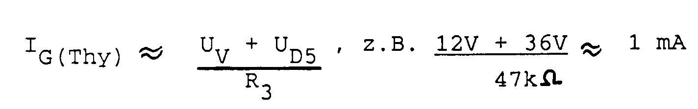
Im Unterschied zur positiven Halbwelle, wo ein vergleichsweise niedriger Gatestrom (ca. 200 µA) fließt, stellt sich hier ein höherer Strom (ca. 1 mA) ein. Dies wirkt sich aber nicht nachteilig aus.The power triac V2 switches off at the beginning of the negative mains half-wave, i.e. at zero crossing. Before he now receives his negative ignition current, the following curve is shown:
The supply voltage U V tries to flow a current into the gate of the thyristor V1 via T1, R3. This actually works because this current can then leave the bridge via D2 and R1 to the phase conductor L, which now has a negative potential. That is, a gate current is set at the thyristor V1 which rises continuously as long as the breakdown voltage of the trigger diode D5 has not yet been reached. Before this point is reached, a resulting gate current (approx. 1 mA) results according to the following approximation equation
In contrast to the positive half-wave, where a comparatively low gate current (approx. 200 µA) flows, a higher current (approx. 1 mA) is set here. However, this does not have an adverse effect.
Bei Erreichen der Triggerspannung, d.h. der Durchbruchspannung der Triggerdiode D5 erhält der Leistungstriac V2 von C1 über D3, D5, V1 und D2 seinen Zündimpuls. Der Leistungstriac V2 bleibt während der negativen Halbwelle leitend.When the trigger voltage is reached, i.e. the breakdown voltage of the trigger diode D5, the power triac V2 receives its ignition pulse from C1 via D3, D5, V1 and D2. The power triac V2 remains conductive during the negative half-wave.
Wird die Triggerdiode D5 zwischen dem Zündkondensator C1 und dem von D1 und D2 gebildeten Wechselspannungsanschluß angeordnet, dann fließt der Gatestrom (von V1) während der positiven und negativen Halbwelle stets in gleicher Höhe (z. B. 200 µA) über R3, V1 und R8, wodurch eine Unsymmetrie weitgehend vermieden wird. Dieser Strom ruft dann am Widerstand R8 einen Spannungsabfall (ca. 50 mV) hervor, wodurch eine vorzeitige Zündung des Leistungstriacs V2 unmöglich ist.If the trigger diode D5 is arranged between the ignition capacitor C1 and the AC voltage connection formed by D1 and D2, the gate current (from V1) always flows at the same level (e.g. 200 μA) via R3, V1 and R8 during the positive and negative half-wave , whereby an asymmetry is largely avoided. This current then causes a voltage drop (approx. 50 mV) across the resistor R8, as a result of which a premature ignition of the power triac V2 is impossible.
Nun folgen einige Anmerkungen zu Besonderheiten der Schaltung.Now there are some comments on the special features of the circuit.
Der Widerstand R1 könnte auch den Wert Null erhalten (100 % Symmetrie). Jedoch ist ein bestimmter Widerstandswert (hier z. B. 10 kΩ ) sinnvoll, um ein unerwünschtes Durchschalten des Bruckenzweiges D5, V1 infolge von Hochspannungsspitzen zu verhindern.Resistor R1 could also have the value zero (100% symmetry). However, a certain resistance value (here, for example, 10 kΩ) is useful in order to prevent undesired switching through of the bridge branch D5, V1 as a result of high-voltage peaks.
Die Kombination R1 - C1 liegt an Netzspannung. Dabei wird der Kondensator C1 abwechselnd positiv und negativ über den Widerstand R1 bis zum Erreichen der Triggerspannung an der Triggerdiode D5 aufgeladen.The combination R1 - C1 is connected to the mains voltage. The capacitor C1 is alternately charged positively and negatively via the resistor R1 until the trigger voltage at the trigger diode D5 is reached.
Während der negativen Netzhalbwelle addieren sich der gemäß Schaltplan durch C1 und der von der Spannungsversorgung her über T1, R3, V1 und D2 fließende Strom. Die Addition der beiden Ströme führt zu einer geringen Unsymmetrie des positiven und negativen Phasenanschnittes (hier 40 V/0,6 ms zu 50 V/0,7 ms). Die Unsymmetrie nimmt mit dem Widerstandsverhältnis ![]()
![]()
Dies gilt allerdings nur, wenn sich die Triggerdiode D5, wie im Schaltbild eingetragen, im Diagonalzweig der Gleichrichter-Brückenschaltung befindet.However, this only applies if the trigger diode D5, as entered in the circuit diagram, is located in the diagonal branch of the rectifier bridge circuit.
Es ist deshalb von Vorteil, wenn die Triggerdiode D5 unmittelbar vor dem ersten Wechselspannungseingang der Gleichrichterbrücke D1 - D4 eingefügt wird. In diesem Fall fließt der Gatestrom des Thyristors V1 während der positiven und negativen Halbwelle in gleicher Höhe von z. B. 200µA über R3, V1, D4 und R8. Hierdurch wird die Unsymmetrie weitgehend vermieden. Dieser Strom ruft an R8 einen Spannungsabfall von ca. 50mV hervor; ein vorzeitiges Zünden des Leistungstriacs V2 ist damit nicht möglich.It is therefore advantageous if the trigger diode D5 is inserted immediately before the first AC voltage input of the rectifier bridge D1-D4. In this case, the gate current of the thyristor V1 flows during the positive and negative half-wave at the same level of z. B. 200µA via R3, V1, D4 and R8. As a result, the asymmetry is largely avoided. This current causes a voltage drop of approx. 50mV at R8; early ignition of the power triac V2 is therefore not possible.
Claims (10)
- Circuit arrangement for controlling a power triac (V2) which is in series with a power supply network-supplied load (6) and applies voltage thereto as a function of the switch position of a control switch (2), said control switch (2) acting on the gate of the power triac (V2) via a drive circuit (1) such that a residual phase-gating angle remains before each occasion when its switching path is switched through and, for this purpose, an RC element (R1, C1), which has a triggering capacitor (C1), supplies the triggering current for the power triac (V2) to the gate of said power triac (V2) via a triggering diode (D5), and such that the AC voltage inputs of a rectifier bridge circuit (D1 to D4) are connected in the current path between the triggering capacitor (C1) and the gate of the power triac (V2) and the current path between the DC voltage outputs of the bridge circuit (D1 to D4) by means of a controllable semiconductor switch (V1) which is connected in the diagonal arm of the bridge circuit and whose gate is initially controlled by the control switch (2), and such that a driver circuit is connected between the gate of the semiconductor switch (V1) and the control switch (2), is supplied from a supply circuit (3) and has a common reference potential (M) with this supply circuit (3), the triggering capacitor (C1), the control switch (2) and with a power circuit breaker (4) which contains the power triac (V2), but not with the rectifier bridge (D1 to D4), and the RC element and the supply circuit (3) being connected between the live conductor (L) of the power supply network and the reference potential (M).
- Circuit arrangement according to Claim 1, characterized in that the driver circuit includes two complementary transistors (T1, T2) of which the collector of the pnp-transistor (T1) is connected via a resistor (R3) at [sic] the gate of the semiconductor switch (V1) and its emitter is connected to the output (UV) of the supply circuit (2), and the emitter of the npn-transistor (T2) is connected to the reference potential while its collector is connected via a resistor (R5) to the base of the pnp-transistor (T2), which base, for its part, is connected via a resistor (R4) to the output (UV) of the supply circuit (3), and the output of the control switch (2) is supplied via a resistor (R6) to the base of the npn-transistor (T2).
- Circuit according to one of the preceding claims, characterized in that the triggering diode (D5) is connected in the diagonal arm of the rectifier bridge (D1 to D4), between the triggering capacitor (C1) and the controllable semiconductor switch (V1).
- Circuit according to one of Claims 1 or 2, characterized in that the triggering diode (D5) is connected between the triggering capacitor (C1) and the first AC voltage input of the rectifier bridge (D1 to D4).
- Circuit arrangement according to one of the preceding claims, characterized in that the controllable semiconductor switch (V1) is a triac or a transistor.
- Circuit arrangement according to one of the preceding claims, characterized in that the semiconductor switch (V1) is a thyristor whose gate is connected via a resistor (R2) and a parallel capacitor (C2) to its cathode.
- Circuit arrangement according to one of the preceding claims, characterized in that the resistor (R1) of the RC element (R1, C1) is connected to the live conductor (L), and the reference potential (M) is connected via the load (6), preferably via one or more incandescent lamps, to the neutral conductor (N) of the power supply network (5).
- Circuit arrangement according to one of the preceding claims, characterized in that the supply circuit (3) is connected to the live conductor (L) by means of a resistor (R7), and is connected to the reference potential (M) by means of a zener diode (D6), in that both are connected by means of a charging capacitor (C3), and in that the anode of a diode (D7) is connected between the charging capacitor (C3) and the zener diode (D6), which diode is connected in series with a buffer capacitor (C4) which is at the reference potential (M), the output (UV) of the supply circuit (3) being connected between the diode (D7) and the buffer capacitor (C4).
- Circuit arrangement according to one of the preceding claims, characterized in that the gate of the power triac (V2) which is contained in the power circuit breaker (4) is connected to the reference potential (M) via a resistor (R8), and a suppression inductor (E), possibly with a fuse (F) in series, is connected to the live conductor (L) in series with the switching path of the power triac (V2).
- Circuit arrangement according to one of the preceding claims, characterized in that a suppression capacitor (C5) is connected between the live conductor (L) and the reference potential (M), and a suppressor diode (D8), which is provided with a bias resistor (R9), is connected in parallel with said suppression capacitor (C5).
Priority Applications (1)
| Application Number | Priority Date | Filing Date | Title |
|---|---|---|---|
| AT88120573T ATE102773T1 (en) | 1987-12-22 | 1988-12-09 | CIRCUIT ARRANGEMENT FOR CONTROLLING A POWER TRIAC. |
Applications Claiming Priority (2)
| Application Number | Priority Date | Filing Date | Title |
|---|---|---|---|
| DE19873743556 DE3743556A1 (en) | 1987-12-22 | 1987-12-22 | CIRCUIT ARRANGEMENT FOR CONTROLLING A PERFORMANCE TRACE |
| DE3743556 | 1987-12-22 |
Publications (3)
| Publication Number | Publication Date |
|---|---|
| EP0321798A2 EP0321798A2 (en) | 1989-06-28 |
| EP0321798A3 EP0321798A3 (en) | 1990-12-27 |
| EP0321798B1 true EP0321798B1 (en) | 1994-03-09 |
Family
ID=6343284
Family Applications (1)
| Application Number | Title | Priority Date | Filing Date |
|---|---|---|---|
| EP88120573A Expired - Lifetime EP0321798B1 (en) | 1987-12-22 | 1988-12-09 | Circuit arrangement for controlling a power triac |
Country Status (6)
| Country | Link |
|---|---|
| EP (1) | EP0321798B1 (en) |
| AT (1) | ATE102773T1 (en) |
| DE (2) | DE3743556A1 (en) |
| DK (1) | DK714188A (en) |
| ES (1) | ES2052680T3 (en) |
| NO (1) | NO172668C (en) |
Families Citing this family (6)
| Publication number | Priority date | Publication date | Assignee | Title |
|---|---|---|---|---|
| DE4117122A1 (en) * | 1991-05-25 | 1992-11-26 | Abb Patent Gmbh | CIRCUIT FOR CONTROLLING AN AC CURRENT |
| HU210725B (en) * | 1994-05-06 | 1995-12-28 | Fazakas | Power controller containing switch with controlled running up/down |
| AUPO778997A0 (en) * | 1997-07-09 | 1997-07-31 | H.P.M. Industries Pty Limited | Solid state switching device circuit |
| AU733423B2 (en) * | 1997-07-09 | 2001-05-17 | H.P.M. Industries Pty Limited | Solid state switching device circuit |
| DE10148644B4 (en) * | 2001-10-02 | 2017-07-27 | Seuffer gmbH & Co. KG | Electrical circuit for dimming the two half-waves of an alternating voltage |
| CN113067570B (en) * | 2021-03-31 | 2023-07-07 | 樊娜 | Electronic wall switch applied to alternating current power supply system |
Citations (5)
| Publication number | Priority date | Publication date | Assignee | Title |
|---|---|---|---|---|
| US3940634A (en) * | 1975-02-14 | 1976-02-24 | Rockwell International Corporation | Solid state AC power relay |
| US4158150A (en) * | 1978-01-10 | 1979-06-12 | Amf Incorporated | Solid state relay with zero crossover feature |
| FR2448805A1 (en) * | 1979-02-08 | 1980-09-05 | Silicium Semiconducteur Ssc | Light dimmer circuit with series triac and inductor - is shunted by oscillation suppressing capacitor in series with resistive voltage divider |
| DE2942662A1 (en) * | 1979-06-28 | 1981-05-07 | Eberhard Dipl.-Phys. 7257 Ditzingen Pechhold | Timed dimmer circuit suitable for stairway lighting - has starter capacitor charged through transistor lying across rectifying bridge |
| EP0244743A2 (en) * | 1986-05-03 | 1987-11-11 | Gebhard Balluff Fabrik feinmechanischer Erzeugnisse GmbH & Co. | Two-wire switch |
Family Cites Families (8)
| Publication number | Priority date | Publication date | Assignee | Title |
|---|---|---|---|---|
| US3862441A (en) * | 1972-11-22 | 1975-01-21 | Mitsubishi Electric Corp | Mos-fet timing circuit |
| US4008416A (en) * | 1973-05-29 | 1977-02-15 | Nakasone Henry H | Circuit for producing a gradual change in conduction angle |
| FR2271712A1 (en) * | 1974-05-15 | 1975-12-12 | Silec Semi Conducteurs | Static electronic device for timing control - is insensitive to parasitic signals and independent of characteristics of static switch |
| GB1527097A (en) * | 1974-11-29 | 1978-10-04 | Omron Tateisi Electronics Co | Solid state switching circuits |
| US4239986A (en) * | 1978-09-08 | 1980-12-16 | Hyrbrinetics, Inc. | Power control arrangement and control circuit especially suitable for use therewith |
| JPS5680929A (en) * | 1979-12-04 | 1981-07-02 | Nippon Gakki Seizo Kk | Triggering circuit for two-way thyristor such as triac |
| JPS59215696A (en) * | 1983-05-21 | 1984-12-05 | 林原 健 | Power source for high intensity bulb |
| US4521705A (en) * | 1983-07-20 | 1985-06-04 | Honeywell Inc. | Reliable field-effect transistor timer circuit |
-
1987
- 1987-12-22 DE DE19873743556 patent/DE3743556A1/en not_active Withdrawn
-
1988
- 1988-12-09 DE DE88120573T patent/DE3888326D1/en not_active Expired - Fee Related
- 1988-12-09 AT AT88120573T patent/ATE102773T1/en active
- 1988-12-09 EP EP88120573A patent/EP0321798B1/en not_active Expired - Lifetime
- 1988-12-09 ES ES88120573T patent/ES2052680T3/en not_active Expired - Lifetime
- 1988-12-20 NO NO885644A patent/NO172668C/en unknown
- 1988-12-21 DK DK714188A patent/DK714188A/en not_active Application Discontinuation
Patent Citations (5)
| Publication number | Priority date | Publication date | Assignee | Title |
|---|---|---|---|---|
| US3940634A (en) * | 1975-02-14 | 1976-02-24 | Rockwell International Corporation | Solid state AC power relay |
| US4158150A (en) * | 1978-01-10 | 1979-06-12 | Amf Incorporated | Solid state relay with zero crossover feature |
| FR2448805A1 (en) * | 1979-02-08 | 1980-09-05 | Silicium Semiconducteur Ssc | Light dimmer circuit with series triac and inductor - is shunted by oscillation suppressing capacitor in series with resistive voltage divider |
| DE2942662A1 (en) * | 1979-06-28 | 1981-05-07 | Eberhard Dipl.-Phys. 7257 Ditzingen Pechhold | Timed dimmer circuit suitable for stairway lighting - has starter capacitor charged through transistor lying across rectifying bridge |
| EP0244743A2 (en) * | 1986-05-03 | 1987-11-11 | Gebhard Balluff Fabrik feinmechanischer Erzeugnisse GmbH & Co. | Two-wire switch |
Also Published As
| Publication number | Publication date |
|---|---|
| NO172668B (en) | 1993-05-10 |
| ATE102773T1 (en) | 1994-03-15 |
| NO885644D0 (en) | 1988-12-20 |
| DK714188A (en) | 1989-06-23 |
| DK714188D0 (en) | 1988-12-21 |
| NO885644L (en) | 1989-06-23 |
| ES2052680T3 (en) | 1994-07-16 |
| EP0321798A3 (en) | 1990-12-27 |
| EP0321798A2 (en) | 1989-06-28 |
| DE3888326D1 (en) | 1994-04-14 |
| DE3743556A1 (en) | 1989-07-13 |
| NO172668C (en) | 1993-08-18 |
Similar Documents
| Publication | Publication Date | Title |
|---|---|---|
| EP0176800B1 (en) | Method and apparatus for controlling the switching condition of a gate turn-off thyristor | |
| DE2738186C3 (en) | Zero switching voltage solid state relay | |
| EP0244743B1 (en) | Two-wire switch | |
| EP0223316A2 (en) | Circuit arrangement for producing a DC voltage from an AC input voltage | |
| DE2263867A1 (en) | CONTROL CIRCUIT FOR THYRISTORS | |
| EP0019813A1 (en) | Electronic on-off touch switch | |
| DE3840406A1 (en) | Protective circuit for a switched-mode power supply circuit | |
| DE2939250C2 (en) | Proximity switch | |
| EP0208065A2 (en) | Circuit arrangement for driving high-voltage power transistors | |
| EP0321798B1 (en) | Circuit arrangement for controlling a power triac | |
| DE3045798A1 (en) | TWO-WAY SWITCH | |
| DE2506196C2 (en) | DC switching device to increase the peak current | |
| EP0219074A2 (en) | Two-wire type switch with a power transistor | |
| DE3917062A1 (en) | LIGHTNING FLASH WARNING SYSTEM | |
| DE4106690A1 (en) | Load control system using insulated-gate bipolar transistor circuit - with overload and short-circuit protection of controlled load | |
| DE1903621A1 (en) | Thyristor control circuit | |
| EP0339598A2 (en) | Protection circuit for capacitives loads | |
| DE60100749T2 (en) | DEFIBRILLATOR | |
| EP0588273A1 (en) | Process for electronically dimming and dimmer for carrying out this process | |
| DE19907942B4 (en) | Speedlight | |
| DE102005020414A1 (en) | Phase control | |
| DE3611724A1 (en) | Brightness controller having a direct-current supply | |
| DE2360392C2 (en) | Device for controlling a thyristor | |
| DE102010018588A1 (en) | Switch-free DIAC replacement circuit | |
| EP2140735B1 (en) | Circuit configuration for starting and operating at least one discharge lamp |
Legal Events
| Date | Code | Title | Description |
|---|---|---|---|
| PUAI | Public reference made under article 153(3) epc to a published international application that has entered the european phase |
Free format text: ORIGINAL CODE: 0009012 |
|
| AK | Designated contracting states |
Kind code of ref document: A2 Designated state(s): AT BE CH DE ES FR GB IT LI NL SE |
|
| PUAL | Search report despatched |
Free format text: ORIGINAL CODE: 0009013 |
|
| AK | Designated contracting states |
Kind code of ref document: A3 Designated state(s): AT BE CH DE ES FR GB IT LI NL SE |
|
| 16A | New documents despatched to applicant after publication of the search report | ||
| 17P | Request for examination filed |
Effective date: 19910605 |
|
| 17Q | First examination report despatched |
Effective date: 19930405 |
|
| GRAA | (expected) grant |
Free format text: ORIGINAL CODE: 0009210 |
|
| AK | Designated contracting states |
Kind code of ref document: B1 Designated state(s): AT BE CH DE ES FR GB IT LI NL SE |
|
| REF | Corresponds to: |
Ref document number: 102773 Country of ref document: AT Date of ref document: 19940315 Kind code of ref document: T |
|
| REF | Corresponds to: |
Ref document number: 3888326 Country of ref document: DE Date of ref document: 19940414 |
|
| GBT | Gb: translation of ep patent filed (gb section 77(6)(a)/1977) |
Effective date: 19940323 |
|
| ET | Fr: translation filed | ||
| ITF | It: translation for a ep patent filed |
Owner name: DE DOMINICIS & MAYER S.R.L. |
|
| REG | Reference to a national code |
Ref country code: ES Ref legal event code: FG2A Ref document number: 2052680 Country of ref document: ES Kind code of ref document: T3 |
|
| PLBE | No opposition filed within time limit |
Free format text: ORIGINAL CODE: 0009261 |
|
| STAA | Information on the status of an ep patent application or granted ep patent |
Free format text: STATUS: NO OPPOSITION FILED WITHIN TIME LIMIT |
|
| EAL | Se: european patent in force in sweden |
Ref document number: 88120573.6 |
|
| 26N | No opposition filed | ||
| PGFP | Annual fee paid to national office [announced via postgrant information from national office to epo] |
Ref country code: GB Payment date: 19961014 Year of fee payment: 9 |
|
| PGFP | Annual fee paid to national office [announced via postgrant information from national office to epo] |
Ref country code: NL Payment date: 19961021 Year of fee payment: 9 |
|
| PGFP | Annual fee paid to national office [announced via postgrant information from national office to epo] |
Ref country code: SE Payment date: 19961024 Year of fee payment: 9 Ref country code: FR Payment date: 19961024 Year of fee payment: 9 Ref country code: AT Payment date: 19961024 Year of fee payment: 9 |
|
| PGFP | Annual fee paid to national office [announced via postgrant information from national office to epo] |
Ref country code: CH Payment date: 19961029 Year of fee payment: 9 |
|
| PGFP | Annual fee paid to national office [announced via postgrant information from national office to epo] |
Ref country code: ES Payment date: 19961224 Year of fee payment: 9 |
|
| PG25 | Lapsed in a contracting state [announced via postgrant information from national office to epo] |
Ref country code: GB Free format text: LAPSE BECAUSE OF NON-PAYMENT OF DUE FEES Effective date: 19971209 Ref country code: AT Free format text: LAPSE BECAUSE OF NON-PAYMENT OF DUE FEES Effective date: 19971209 |
|
| PG25 | Lapsed in a contracting state [announced via postgrant information from national office to epo] |
Ref country code: SE Free format text: LAPSE BECAUSE OF NON-PAYMENT OF DUE FEES Effective date: 19971210 Ref country code: ES Free format text: LAPSE BECAUSE OF EXPIRATION OF PROTECTION Effective date: 19971210 |
|
| PG25 | Lapsed in a contracting state [announced via postgrant information from national office to epo] |
Ref country code: LI Free format text: LAPSE BECAUSE OF NON-PAYMENT OF DUE FEES Effective date: 19971231 Ref country code: FR Free format text: THE PATENT HAS BEEN ANNULLED BY A DECISION OF A NATIONAL AUTHORITY Effective date: 19971231 Ref country code: CH Free format text: LAPSE BECAUSE OF NON-PAYMENT OF DUE FEES Effective date: 19971231 |
|
| PG25 | Lapsed in a contracting state [announced via postgrant information from national office to epo] |
Ref country code: NL Free format text: LAPSE BECAUSE OF NON-PAYMENT OF DUE FEES Effective date: 19980701 |
|
| GBPC | Gb: european patent ceased through non-payment of renewal fee |
Effective date: 19971209 |
|
| REG | Reference to a national code |
Ref country code: CH Ref legal event code: PL |
|
| NLV4 | Nl: lapsed or anulled due to non-payment of the annual fee |
Effective date: 19980701 |
|
| EUG | Se: european patent has lapsed |
Ref document number: 88120573.6 |
|
| REG | Reference to a national code |
Ref country code: FR Ref legal event code: ST |
|
| PGFP | Annual fee paid to national office [announced via postgrant information from national office to epo] |
Ref country code: BE Payment date: 19981109 Year of fee payment: 11 |
|
| PG25 | Lapsed in a contracting state [announced via postgrant information from national office to epo] |
Ref country code: BE Free format text: LAPSE BECAUSE OF NON-PAYMENT OF DUE FEES Effective date: 19991231 |
|
| BERE | Be: lapsed |
Owner name: ASEA BROWN BOVERI A.G. Effective date: 19991231 |
|
| REG | Reference to a national code |
Ref country code: ES Ref legal event code: FD2A Effective date: 20010201 |
|
| PGFP | Annual fee paid to national office [announced via postgrant information from national office to epo] |
Ref country code: DE Payment date: 20041213 Year of fee payment: 17 |
|
| PG25 | Lapsed in a contracting state [announced via postgrant information from national office to epo] |
Ref country code: IT Free format text: LAPSE BECAUSE OF NON-PAYMENT OF DUE FEES;WARNING: LAPSES OF ITALIAN PATENTS WITH EFFECTIVE DATE BEFORE 2007 MAY HAVE OCCURRED AT ANY TIME BEFORE 2007. THE CORRECT EFFECTIVE DATE MAY BE DIFFERENT FROM THE ONE RECORDED. Effective date: 20051209 |
|
| PG25 | Lapsed in a contracting state [announced via postgrant information from national office to epo] |
Ref country code: DE Free format text: LAPSE BECAUSE OF NON-PAYMENT OF DUE FEES Effective date: 20060701 |