EP2140735B1 - Circuit configuration for starting and operating at least one discharge lamp - Google Patents
Circuit configuration for starting and operating at least one discharge lamp Download PDFInfo
- Publication number
- EP2140735B1 EP2140735B1 EP07728402A EP07728402A EP2140735B1 EP 2140735 B1 EP2140735 B1 EP 2140735B1 EP 07728402 A EP07728402 A EP 07728402A EP 07728402 A EP07728402 A EP 07728402A EP 2140735 B1 EP2140735 B1 EP 2140735B1
- Authority
- EP
- European Patent Office
- Prior art keywords
- coupled
- circuit
- transistor
- auxiliary transistor
- secondary winding
- Prior art date
- Legal status (The legal status is an assumption and is not a legal conclusion. Google has not performed a legal analysis and makes no representation as to the accuracy of the status listed.)
- Not-in-force
Links
Images
Classifications
-
- H—ELECTRICITY
- H05—ELECTRIC TECHNIQUES NOT OTHERWISE PROVIDED FOR
- H05B—ELECTRIC HEATING; ELECTRIC LIGHT SOURCES NOT OTHERWISE PROVIDED FOR; CIRCUIT ARRANGEMENTS FOR ELECTRIC LIGHT SOURCES, IN GENERAL
- H05B41/00—Circuit arrangements or apparatus for igniting or operating discharge lamps
- H05B41/14—Circuit arrangements
- H05B41/26—Circuit arrangements in which the lamp is fed by power derived from dc by means of a converter, e.g. by high-voltage dc
- H05B41/28—Circuit arrangements in which the lamp is fed by power derived from dc by means of a converter, e.g. by high-voltage dc using static converters
- H05B41/282—Circuit arrangements in which the lamp is fed by power derived from dc by means of a converter, e.g. by high-voltage dc using static converters with semiconductor devices
- H05B41/2825—Circuit arrangements in which the lamp is fed by power derived from dc by means of a converter, e.g. by high-voltage dc using static converters with semiconductor devices by means of a bridge converter in the final stage
-
- Y—GENERAL TAGGING OF NEW TECHNOLOGICAL DEVELOPMENTS; GENERAL TAGGING OF CROSS-SECTIONAL TECHNOLOGIES SPANNING OVER SEVERAL SECTIONS OF THE IPC; TECHNICAL SUBJECTS COVERED BY FORMER USPC CROSS-REFERENCE ART COLLECTIONS [XRACs] AND DIGESTS
- Y10—TECHNICAL SUBJECTS COVERED BY FORMER USPC
- Y10S—TECHNICAL SUBJECTS COVERED BY FORMER USPC CROSS-REFERENCE ART COLLECTIONS [XRACs] AND DIGESTS
- Y10S315/00—Electric lamp and discharge devices: systems
- Y10S315/05—Starting and operating circuit for fluorescent lamp
-
- Y—GENERAL TAGGING OF NEW TECHNOLOGICAL DEVELOPMENTS; GENERAL TAGGING OF CROSS-SECTIONAL TECHNOLOGIES SPANNING OVER SEVERAL SECTIONS OF THE IPC; TECHNICAL SUBJECTS COVERED BY FORMER USPC CROSS-REFERENCE ART COLLECTIONS [XRACs] AND DIGESTS
- Y10—TECHNICAL SUBJECTS COVERED BY FORMER USPC
- Y10S—TECHNICAL SUBJECTS COVERED BY FORMER USPC CROSS-REFERENCE ART COLLECTIONS [XRACs] AND DIGESTS
- Y10S315/00—Electric lamp and discharge devices: systems
- Y10S315/07—Starting and control circuits for gas discharge lamp using transistors
Definitions
- the present invention relates to a circuit arrangement for igniting and operating at least one discharge lamp having a first and a second input terminal for connecting a supply voltage, an inverter comprising at least a first and a second main transistor in a half-bridge arrangement, which is coupled in series between the first and the second input terminal a first and a second output terminal for connecting the at least one discharge lamp, at least one lamp inductor coupled in series with the first output terminal, at least one output capacitor coupled in parallel with the first and second output terminals, a transformer having a primary winding and a first one and a second secondary winding, wherein a series circuit comprising the primary winding and the at least one lamp inductor is coupled between the half-bridge center and a reference potential; and a first control circuit for driving the first main transistor and a second control circuit for driving the second main transistor, wherein each control circuit has an input and an output, wherein the output of the first control circuit to the control electrode of the first main transistor and the output of the second control circuit to the control electrode the second
- the frequency-dependent voltage divider of each time circuit comprises an ohmic resistance and a capacitor, wherein the voltage dropping across the capacitor is coupled to the control path of the first auxiliary transistor.
- Zener diodes are provided which are used as relatively accurate thresholds for generating the blanking voltage for the discharge lamp, ie the voltage available across the lamp for ignition.
- the current-limiting effect of the lamp choke is due to a possible saturation back, whereby the main transistors of the inverter can be destroyed. It should be noted, however, that operation of the lamp choke with light saturation is desirable because this results in low losses. Exactly at the point makes an increase in tolerances then negatively noticeable, since thereby the danger the saturation of the lamp choke is created. As a result, this would result in a reduction of the control losses in a greater dimensioning of the components of the circuit arrangement and thus in higher costs.
- the present invention is therefore based on the object, the above-mentioned circuit arrangement such that a reduction of tax losses without risk of destruction of the main transistors of the inverter or without necessity, the main transistors of the inverter is more strongly dimensioned.
- the present invention is based on the finding that a disadvantage of the prior art is that the capacitor of the frequency-dependent voltage divider is also problematic because it acts as an energy store at the control electrode of the first auxiliary transistor and thus by its charge and discharge an undesirable delay the voltage at the control electrode of the first auxiliary transistor relative to the current in the control electrode of the main transistor is formed.
- the frequency-dependent voltage divider is realized in an inventive circuit arrangement by an inductor and a resistor, wherein the voltage dropping across the ohmic resistor is coupled to the control path of the first auxiliary transistor.
- the Z-diodes affected by the above-mentioned disadvantages are replaced by a second Auxiliary transistor is connected in parallel with the inductance of the frequency-dependent voltage divider, wherein the second auxiliary transistor comprises a drive circuit which is designed to bridge the associated inductance in dependence on the voltage at the associated secondary winding by the second auxiliary transistor.
- transistors used for the second auxiliary transistor usually switch at a voltage of 0.6 to 0.7V on the control path, that is, at such a voltage between the control and reference electrodes, whereas the already mentioned above Z-diode voltages by a factor of 10 over.
- a preferred embodiment is characterized in that the second mentioned measure according to the invention, ie the measure which provides a second auxiliary transistor, which is connected in parallel with the associated inductance, is provided only in one of the two time circuits. This is particularly possible in load circuits of low operating quality, in which the difference between the ignition frequency and operating frequency is low and in which the lamp inductor is operated only slightly saturated when ignited.
- the at least one second auxiliary transistor comprises a control electrode, a working electrode and a reference electrode, wherein the working electrode is coupled to the point of the associated voltage divider, at which the inductance is coupled to the ohmic resistance, wherein the reference electrode with the associated second Secondary winding is coupled.
- the at least one timing circuit further comprises a current measuring resistor which is serially coupled between the associated secondary winding and the output of the associated timing circuit, wherein the voltage dropping across the current sensing resistor is coupled to the control electrode of the associated second auxiliary transistor.
- the voltage which switches the second auxiliary transistor on and off is made dependent on the current in the control electrode of the respective main transistor.
- a first further ohmic resistance is coupled between the working electrode of the at least one second auxiliary transistor and the point of the associated voltage divider, at which the inductance is coupled to the ohmic resistance.
- An ohmic resistor provided at this point acts as a current limiting resistor and thus ensures that the current driven by the transformer continues to flow essentially through the current measuring resistor and thus keeps the second auxiliary transistor safely open.
- a capacitor is coupled between the point at which the inductance of the respective voltage divider is coupled to the respective secondary winding, and the respective inductance.
- a second further ohmic resistance is coupled between the current measuring resistor and the output of the associated timing circuit.
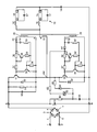
- the figure shows a circuit arrangement according to the invention and a supply arrangement for this circuit arrangement and two lamps which are ignited or fed by means of this circuit arrangement.
- the supply arrangement comprises two input terminals 1 and 2, which are intended for connection to an AC voltage source.
- a rectifier bridge 3 with four diodes (4 to 7 inclusive) is connected.
- a filter between the input terminals 1 and 2 on the one hand, and the rectifier bridge 3 on the other hand, may be provided.
- An output terminal of the rectifier bridge 3 is connected to a first input terminal A of the circuit arrangement.
- a second output terminal of the rectifier bridge 3 is connected to an input terminal B of the circuit arrangement.
- the terminals A and B are connected by a capacitor 10 and also by a series connection of a first main transistor 11, a primary winding 12 of a current transformer and a load circuit 13, the details of which are listed below, and a capacitor 14.
- the load circuit 13 comprises two substantially equal, parallel branches. Each of these branches comprises a discharge lamp 15 or 15 ', connected in series with a lamp choke 16 or 16'.
- Each of the lamps 15, 15 ' has two preheatable electrodes. Belonging to a lamp 15, 15 'remote from a supply source electrode ends are connected by an output capacitor 17 and 17' to each other.
- Each of these output capacitors 17, 17 'therefore represents a circuit element connected in parallel with the relevant lamp 15, 15'.
- the series connection of the primary winding 12 of the transformer, the load circuit 13 and the capacitor 14 is connected in parallel with a second main transistor 20.
- Each of the two main transistors 11 and 20 is of the NPN type.
- the collector of the main transistor 11 is connected to the positive input terminal A of the circuit arrangement.
- the emitter of this main transistor 11 is connected to the collector of the main transistor 20.
- the emitter of this main transistor 20 is connected to the negative input terminal B of the circuit arrangement.
- current negative feedback resistors in particular emitter resistors, may be provided for the main transistors 11 and 20.
- the main transistors 11 and 20 in half-bridge arrangement is defines a half-bridge center HM.
- the current transformer having the primary winding 12 has two secondary windings 30 and 31, respectively.
- the secondary winding 30 is connected to a control circuit of the main transistor 11.
- the secondary winding 31 is connected to a control circuit of the main transistor 20.
- the control circuits are substantially similar to each other.
- the ends of the secondary winding 30 are connected to each other via a diode 40 and a timing circuit comprising a series circuit of a capacitor 32, an inductor 33 and an ohmic resistor 34.
- the timing circuit further comprises a first auxiliary transistor 35 whose base is connected to the connection point between the capacitor 32 and the inductor 33 on the one hand and the ohmic resistor 34 on the other.
- a second auxiliary transistor 38 is provided, whose collector-emitter path is connected in parallel with a series resistor ohmic resistance 39 of the series circuit of capacitor 32 and inductance 33 arranged in parallel therewith.
- an ohmic resistor 36 is connected, which serves as a current measuring resistor.
- a second further ohmic resistor 37 is connected in series between the ohmic resistor 36 and the base of the main transistor 11.
- a corresponding timing circuit 32 'to 40' connects the ends of the secondary winding 31 with each other.
- a diode 50 is connected in anti-parallel to the main transistor 11.
- a diode 50 ' is connected in anti-parallel to the main transistor 20.
- Parallel to the main transistor 11 is still an ohmic resistor 51 and a capacitor 52 connected.
- a circuit for starting the circuit comprises inter alia a series connection of a resistor 60 and a capacitor 61, which is connected in parallel with the capacitor 10.
- a connection point between the resistor 60 and the capacitor 61 is connected to a bi-directional threshold element 62, in the present case a DIAC.
- the other side of this threshold element 62 is connected via a resistor 63 to a point between the resistor 36 'and the diode 40' of the control circuit of the main transistor 20.
- the node between the resistor 60 and the capacitor 61 is also connected to a diode 64.
- the other side of this diode 64 is connected via a resistor 65 to the collector of the main transistor 20.
- the circuit described operates as follows:
- the terminals 1 and 2 are connected to an AC voltage of, for example, 230 V, 50 Hz.
- a DC voltage is applied through the rectifier bridge 3 between the terminals A and B of the circuit arrangement. Consequently, current first flows from A through resistor 51, primary winding 12 of the current transformer, load circuit 13, and capacitor 14 to terminal B, causing the output capacitors 17, 17 'and capacitor 14 to charge.
- the capacitor 61 is charged via the resistor 60.
- the threshold voltage of the threshold element 62 is then reached, the capacitor 61 becomes, inter alia, via the resistors 63, 36 ', 37' and the base-emitter junction of the main transistor 20 discharged.
- This discharge process ensures that the main transistor 20 becomes conductive for the first time.
- the capacitor 14 in the circuit 14, 13, 12, 20, 14 is discharged. Since this discharge current also flows through the primary winding 12 of the current transformer, voltages in the two secondary windings 30 and 31 are induced. The induced voltage in the winding 31 has a sense of direction holding the main transistor 20 in a conducting state.
- the elements 32 ', 33', 34 'of the timing circuit turn on the first auxiliary transistor 35' after elapse of a predetermined period of time. As a result, the main transistor 20 becomes non-conductive.
- the current of the load circuit 13 then flows through the combination of the diode 50 and the capacitor 52 and through the capacitor 10 back to the capacitor 14.
- the lamps 15, 15 ' are then not ignited.
- the load circuit 13 in this case comprises a parallel connection of two practically identical branches, each of which consists of a series connection of a lamp inductor 16 and an output capacitor 17 (or 16 'and 17'). This circuit is not attenuated by the lamps 15, 15 '. Without the presence of the second auxiliary transistors 38 and 38 'in the timing circuits, the frequency of the current flowing through the load circuit 13 would be set practically at the resonant frequency of that circuit. As a result, such great voltages would be applied to the lamps 15 and 15 'that they would ignite with cold cathodes. In the case of defective lamps, this could also lead to an electrically inadmissible situation in the circuit 13 due to very high currents.
- the time constant of the timing is influenced, in this case, by the fact that the series circuit of capacitor 32 and inductor 33 and 32 'and 33' is bridged by the ohmic resistor 39.
- the voltage across the ohmic resistor 34 or 34 ' more quickly reaches the value at which the auxiliary transistor 35 or 35' becomes conductive, with the result that the associated main transistor 11 or 20 becomes nonconductive more rapidly. This causes the frequency of the circuit arrangement to reach a higher value.
Abstract
Description
Die vorliegende Erfindung betrifft eine Schaltungsanordnung zum Zünden und Betreiben mindestens einer Entladungslampe mit einem ersten und einem zweiten Eingangsanschluss zum Anschließen einer Versorgungsspannung, einem Wechselrichter, der mindestens einen ersten und einen zweiten Haupttransistor in Halbbrückenanordnung umfasst, die seriell zwischen den ersten und den zweiten Eingangsanschluss gekoppelt sind, einem ersten und einem zweiten Ausgangsanschluss zum Anschließen der mindestens einen Entladungslampe, mindestens einer Lampendrossel, die seriell zum ersten Ausgangsanschluss gekoppelt ist, mindestens einem Ausgangskondensator, der parallel zum ersten und zum zweiten Ausgangsanschluss gekoppelt ist, einem Transformator mit einer Primärwicklung und einer ersten und einer zweiten Sekundärwicklung, wobei eine Serienschaltung, die die Primärwicklung und die mindestens eine Lampendrossel umfasst zwischen den Halbbrückenmittelpunkt und ein Bezugspotential gekoppelt ist; und einer ersten Steuerschaltung zur Ansteuerung des ersten Haupttransistors und einer zweiten Steuerschaltung zur Ansteuerung des zweiten Haupttransistors, wobei jede Steuerschaltung einen Eingang und einen Ausgang aufweist, wobei der Ausgang der ersten Steuerschaltung mit der Steuerelektrode des ersten Haupttransistors und der Ausgang der zweiten Steuerschaltung mit der Steuerelektrode des zweiten Haupttransistors gekoppelt ist, wobei der Eingang der ersten Steuerschaltung mit der ersten Sekundärwicklung und der Eingang der zweiten Steuerschaltung mit der zweiten Sekundärwicklung gekoppelt ist, wobei jede Steuerschaltung eine Zeitschaltung aufweist, deren Zeitkonstante in Abhängigkeit von der am Eingang der jeweiligen Steuerschaltung anliegenden Spannung variiert, wobei jede Zeitschaltung zumindest einen ersten Hilfstransistor aufweist, wobei die Arbeitselektrode des ersten Hilfstransistors mit der Steuerelektrode des zugehörigen Haupttransistors und die Bezugselektrode des ersten Hilfstransistors mit einem Bezugspotential gekoppelt ist, wobei die Steuerelektrode des ersten Hilfstransistors mit dem Mittelpunkt eines frequenzabhängigen Spannungsteilers gekoppelt ist, der einerseits mit der jeweiligen Sekundärwicklung, andererseits mit dem jeweiligen Bezugspotential gekoppelt ist.The present invention relates to a circuit arrangement for igniting and operating at least one discharge lamp having a first and a second input terminal for connecting a supply voltage, an inverter comprising at least a first and a second main transistor in a half-bridge arrangement, which is coupled in series between the first and the second input terminal a first and a second output terminal for connecting the at least one discharge lamp, at least one lamp inductor coupled in series with the first output terminal, at least one output capacitor coupled in parallel with the first and second output terminals, a transformer having a primary winding and a first one and a second secondary winding, wherein a series circuit comprising the primary winding and the at least one lamp inductor is coupled between the half-bridge center and a reference potential; and a first control circuit for driving the first main transistor and a second control circuit for driving the second main transistor, wherein each control circuit has an input and an output, wherein the output of the first control circuit to the control electrode of the first main transistor and the output of the second control circuit to the control electrode the second main transistor is coupled, wherein the input of the first control circuit to the first secondary winding and the input of the second control circuit is coupled to the second secondary winding, each control circuit having a timing whose time constant varies in response to the voltage applied to the input of the respective control circuit, each timing circuit having at least a first auxiliary transistor, the working electrode of the first auxiliary transistor is coupled to the control electrode of the associated main transistor and the reference electrode of the first auxiliary transistor to a reference potential, wherein the control electrode of the first auxiliary transistor is coupled to the center of a frequency-dependent voltage divider which is coupled on the one hand to the respective secondary winding, on the other hand to the respective reference potential.
Eine derartige Schaltungsanordnung ist bekannt aus der
Aus der Schrift
Die strombegrenzende Wirkung der Lampendrossel geht infolge einer möglicherweise auftretenden Sättigung zurück, wodurch die Haupttransistoren des Wechselrichters zerstört werden können. Hierbei ist zu berücksichtigen, dass ein Betrieb der Lampendrossel mit leichter Sättigung jedoch erwünscht ist, da dies in niedrigen Verlusten resultiert. Genau an der Stelle macht sich eine Erhöhung der Toleranzen dann negativ bemerkbar, da dadurch die Gefahr der Sättigung der Lampendrossel geschaffen wird. In der Folge würde auf diesem Wege eine Reduktion der Steuerverluste in einer stärkeren Dimensionierung der Bauteile der Schaltungsanordnung resultieren und damit in höheren Kosten.The current-limiting effect of the lamp choke is due to a possible saturation back, whereby the main transistors of the inverter can be destroyed. It should be noted, however, that operation of the lamp choke with light saturation is desirable because this results in low losses. Exactly at the point makes an increase in tolerances then negatively noticeable, since thereby the danger the saturation of the lamp choke is created. As a result, this would result in a reduction of the control losses in a greater dimensioning of the components of the circuit arrangement and thus in higher costs.
Der vorliegenden Erfindung liegt deshalb die Aufgabe zugrunde, die eingangs genannte Schaltungsanordnung derart weiterzubilden, dass eine Reduktion der Steuerverlüste ohne Gefahr einer Zerstörung der Haupttransistoren der Wechselrichter bzw. ohne Notwendigkeit die Haupttransistoren des Wechselrichters stärker zu dimensionieren ermöglicht wird.The present invention is therefore based on the object, the above-mentioned circuit arrangement such that a reduction of tax losses without risk of destruction of the main transistors of the inverter or without necessity, the main transistors of the inverter is more strongly dimensioned.
Diese Aufgabe wird gelöst durch eine Schaltungsanordnung mit den Merkmalen von Patentanspruch 1.This object is achieved by a circuit arrangement having the features of
Die vorliegende Erfindung basiert auf der Erkenntnis, dass ein Nachteil beim Stand der Technik darin besteht, dass der Kondensator des frequenzabhängigen Spannungsteilers auch deshalb problematisch ist, da er als Energiespeicher an der Steuerelektrode des ersten Hilfstransistors wirkt und damit durch dessen Ladung und Entladung eine unerwünschte Verzögerung der Spannung an der Steuerelektrode des ersten Hilfstransistors gegenüber dem Strom in die Steuerelektrode des Haupttransistors entsteht. Auf der Basis dieser Erkenntnis wird der frequenzabhängige Spannungsteiler bei einer erfindungsgemäßen Schaltungsanordnung durch eine Induktivität und einen ohmschen Widerstand realisiert, wobei die am ohmschen Widerstand abfallende Spannung an die Steuerstrecke des ersten Hilfstransistors gekoppelt wird. Durch diese Maßnahme ist die Steuerelektrode des ersten Hilfstransistors nicht mehr in unerwünschter Weise mit einem Energiespeicher gekoppelt, unerwünschte Verzögerungen damit eliminiert. Als zweite Maßnahme werden die mit den oben bereits erwähnten Nachteilen behafteten Z-Dioden ersetzt, indem ein zweiter Hilfstransistor zu der Induktivität des frequenzabhängigen Spannungsteilers parallel geschaltet wird, wobei der zweite Hilfstransistor eine Ansteuerschaltung umfasst, die ausgelegt ist, die zugehörige Induktivität in Abhängigkeit der Spannung an der zugehörigen Sekundärwicklung durch den zweiten Hilfstransistor zu überbrücken. Dabei ist zu berücksichtigen, dass Transistoren, die für den zweiten Hilfstransistor verwendet werden, üblicherweise bei einer Spannung von 0,6 bis 0,7 V an der Steuerstrecke, d. h. bei einer derartigen Spannung zwischen der Steuer- und der Bezugselektrode, schalten, wohingegen die oben bereits erwähnten Z-Dioden-Spannungen um den Faktor 10 darüber liegen.The present invention is based on the finding that a disadvantage of the prior art is that the capacitor of the frequency-dependent voltage divider is also problematic because it acts as an energy store at the control electrode of the first auxiliary transistor and thus by its charge and discharge an undesirable delay the voltage at the control electrode of the first auxiliary transistor relative to the current in the control electrode of the main transistor is formed. On the basis of this finding, the frequency-dependent voltage divider is realized in an inventive circuit arrangement by an inductor and a resistor, wherein the voltage dropping across the ohmic resistor is coupled to the control path of the first auxiliary transistor. By this measure, the control electrode of the first auxiliary transistor is no longer undesirably coupled to an energy storage, eliminating unwanted delays. As a second measure, the Z-diodes affected by the above-mentioned disadvantages are replaced by a second Auxiliary transistor is connected in parallel with the inductance of the frequency-dependent voltage divider, wherein the second auxiliary transistor comprises a drive circuit which is designed to bridge the associated inductance in dependence on the voltage at the associated secondary winding by the second auxiliary transistor. It should be noted that transistors used for the second auxiliary transistor usually switch at a voltage of 0.6 to 0.7V on the control path, that is, at such a voltage between the control and reference electrodes, whereas the already mentioned above Z-diode voltages by a factor of 10 over.
Durch die erfindungsgemäße Konfiguration lässt sich mit wenigen, sehr preiswerten Standardbauteilen eine gute Reproduzierbarkeit der Leerspannung und der Betriebsparameter, d. h. der Parameter für den Dauerbetrieb der Entladungslampe, bei gleichzeitig deutlich verringerten Steuerverlusten gewährleisten. In einem realisierten Ausführungsbeispiel konnten die Steuerverluste um ca. 80 % reduziert werden.By virtue of the configuration according to the invention, good reproducibility of the empty voltage and the operating parameters can be achieved with a few, very inexpensive standard components. H. ensure the parameter for the continuous operation of the discharge lamp, at the same time significantly reduced control losses. In a realized embodiment, the tax losses could be reduced by about 80%.
Eine bevorzugte Ausführungsform zeichnet sich dadurch aus, dass die zweite erwähnte erfindungsgemäße Maßnahme, d. h. die Maßnahme, die einen zweiten Hilfstransistor vorsieht, der zur zugehörigen Induktivität parallel geschaltet ist, nur in einer der beiden Zeitschaltungen vorgesehen ist. Dies ist insbesondere möglich bei Lastkreisen geringer Betriebsgüte, bei denen die Differenz zwischen Zündfrequenz und Betriebsfrequenz gering ist und bei denen die Lampendrossel beim Zünden nur wenig gesättigt betrieben wird.A preferred embodiment is characterized in that the second mentioned measure according to the invention, ie the measure which provides a second auxiliary transistor, which is connected in parallel with the associated inductance, is provided only in one of the two time circuits. This is particularly possible in load circuits of low operating quality, in which the difference between the ignition frequency and operating frequency is low and in which the lamp inductor is operated only slightly saturated when ignited.
In einer bevorzugten Ausführungsform weist der mindestens eine zweite Hilfstransistor eine Steuerelektrode, eine Arbeitselektrode und eine Bezugselektrode auf, wobei die Arbeitselektrode mit dem Punkt des zugehörigen Spannungsteilers gekoppelt ist, an dem die Induktivität mit dem ohmschen Widerstand gekoppelt ist, wobei die Bezugselektrode mit der zugehörigen zweiten Sekundärwicklung gekoppelt ist. Durch diese Verschaltung wird auf einfache Weise sichergestellt, dass die Induktivität des frequenzabhängigen Spannungsteilers durch den zweiten Hilfstransistor überbrückt werden kann, sofern der zweite Hilfstransistor leitend geschaltet wird.In a preferred embodiment, the at least one second auxiliary transistor comprises a control electrode, a working electrode and a reference electrode, wherein the working electrode is coupled to the point of the associated voltage divider, at which the inductance is coupled to the ohmic resistance, wherein the reference electrode with the associated second Secondary winding is coupled. By this interconnection is ensured in a simple manner that the inductance of the frequency-dependent voltage divider can be bypassed by the second auxiliary transistor, provided that the second auxiliary transistor is turned on.
Weiterhin ist bevorzugt, dass die mindestens eine Zeitschaltung weiterhin einen Strommesswiderstand umfasst, der seriell zwischen die zugehörige Sekundärwicklung und den Ausgang der zugehörigen Zeitschaltung gekoppelt ist, wobei die am Strommesswiderstand abfallende Spannung an die Steuerelektrode des zugehörigen zweiten Hilfstransistors gekoppelt ist. Dadurch wird die den zweiten Hilfstransistor ein- und ausschaltende Spannung vom Strom in die Steuerelektrode des jeweiligen Haupttransistors abhängig gemacht. Damit lässt sich erreichen, dass eine Überbrückung der Induktivität des frequenzabhängigen Spannungsteilers sehr genau mit dem zeitlichen Verlauf des Stroms in die Steuerelektrode des jeweiligen Haupttransistors verknüpft ist, der wiederum aufgrund der Auslegung des Transformators als Stromtransformator ein Abbild des Lastkreisstroms ist. Unerwünschte zeitliche Toleranzen wie im Stand der Technik, die versehentlich eine Sättigung der Lampendrossel bewirken könnten, werden damit zuverlässig ausgeschlossen.Furthermore, it is preferred that the at least one timing circuit further comprises a current measuring resistor which is serially coupled between the associated secondary winding and the output of the associated timing circuit, wherein the voltage dropping across the current sensing resistor is coupled to the control electrode of the associated second auxiliary transistor. As a result, the voltage which switches the second auxiliary transistor on and off is made dependent on the current in the control electrode of the respective main transistor. This makes it possible to achieve that a bridging of the inductance of the frequency-dependent voltage divider is very closely linked to the time profile of the current in the control electrode of the respective main transistor, which in turn is an image of the load circuit current due to the design of the transformer as a current transformer. Undesirable time tolerances as in the prior art, which could cause accidental saturation of the lamp inductor are thus reliably excluded.
Bevorzugt ist weiterhin vorgesehen, dass zwischen die Arbeitselektrode des mindestens einen zweiten Hilfstransistors und den Punkt des zugehörigen Spannungsteilers, an dem die Induktivität mit dem ohmschen Widerstand gekoppelt ist, ein erster weiterer ohmscher Widerstand gekoppelt ist. Ein an dieser Stelle vorgesehener ohmscher Widerstand wirkt als Strombegrenzungswiderstand und stellt damit sicher, dass der vom Transformator getriebene Strom weiterhin im Wesentlichen durch den Strommesswiderstand fließt und damit den zweiten Hilfstransistor sicher aufgesteuert hält.Preferably, it is further provided that between the working electrode of the at least one second auxiliary transistor and the point of the associated voltage divider, at which the inductance is coupled to the ohmic resistance, a first further ohmic resistance is coupled. An ohmic resistor provided at this point acts as a current limiting resistor and thus ensures that the current driven by the transformer continues to flow essentially through the current measuring resistor and thus keeps the second auxiliary transistor safely open.
Bevorzugt ist weiterhin vorgesehen, dass zwischen dem Punkt, an dem die Induktivität des jeweiligen Spannungsteilers mit der jeweiligen Sekundärwicklung gekoppelt ist, und die jeweilige Induktivität ein Kondensator gekoppelt ist. Durch diese Maßnahme wird eine Sättigung der Induktivität des frequenzabhängigen Spannungsteilers für den Fall zuverlässig verhindert, in dem die von der zugehörigen Sekundärwicklung in die Steuerschaltung eingespeiste Spannung einen Gleichanteil aufweist. Dabei ist darauf zu achten, dass der Kondensator groß genug gewählt wird, so dass die durch den ohmschen Widerstand und die Induktivität des frequenzabhängigen Spannungsteilers festgelegte Zeitkonstante nicht verändert wird.Preferably, it is further provided that between the point at which the inductance of the respective voltage divider is coupled to the respective secondary winding, and the respective inductance, a capacitor is coupled. By this measure, a saturation of the inductance of the frequency-dependent voltage divider is reliably prevented for the case in which the voltage fed by the associated secondary winding into the control circuit voltage has a DC component. It is important to ensure that the capacitor is chosen large enough, so that the fixed by the ohmic resistance and the inductance of the frequency-dependent voltage divider time constant is not changed.
Schließlich ist weiterhin bevorzugt, dass zwischen den Strommesswiderstand und den Ausgang der zugehörigen Zeitschaltung ein zweiter weiterer ohmscher Widerstand gekoppelt ist. Durch diese Maßnahme fällt an beiden Widerständen im Lampenbetrieb wiederum genügend Spannung ab, damit auch am Widerstand des frequenzabhängigen Spannungsteilers die Basis-Emitter-Flußspannung des ersten Hilfstransistors sicher erreicht wird und die Rückkopplung ausreichend groß ist.Finally, it is further preferred that a second further ohmic resistance is coupled between the current measuring resistor and the output of the associated timing circuit. By this measure, sufficient voltage drops again at both resistors in the lamp operation, thus also at the resistance of the frequency-dependent voltage divider, the base-emitter-forward voltage of the first auxiliary transistor safely achieved and the feedback is sufficiently large.
Weitere vorteilhafte Ausführungsformen ergeben sich aus den Unteransprüchen.Further advantageous embodiments will become apparent from the dependent claims.
Im Nachfolgenden wird nunmehr ein Ausführungsbeispiel einer erfindungsgemäßen Schaltungsanordnung unter Bezugnahme auf die beigefügte Zeichnung näher beschrieben, die in schematischer Darstellung ein Ausführungsbeispiel einer erfindungsgemäßen Schaltungsanordnung zeigt.In the following, an embodiment of a circuit arrangement according to the invention will now be described in more detail with reference to the accompanying drawing, which shows a schematic representation of an embodiment of a circuit arrangement according to the invention.
Die Figur zeigt eine erfindungsgemäße Schaltungsanordnung und eine Versorgungsanordnung für diese Schaltungsanordnung sowie zwei Lampen, die mithilfe dieser Schaltungsanordnung gezündet bzw. gespeist werden. Die Versorgungsanordnung umfasst zwei Eingangsanschlüsse 1 und 2, die zum Anschluss an eine Wechselspannungsquelle bestimmt sind. An diese Anschlüsse 1 und 2 ist eine Gleichrichterbrücke 3 mit vier Dioden (4 bis einschließlich 7) angeschlossen. Es kann des Weiteren beispielsweise ein Filter zwischen den Eingangsanschlüssen 1 und 2 einerseits, und der Gleichrichterbrücke 3 andererseits, vorgesehen sein. Ein Ausgangsanschluss der Gleichrichterbrücke 3 ist mit einem ersten Eingangsanschluss A der Schaltungsanordnung verbunden. Ein zweiter Ausgangsanschluss der Gleichrichterbrücke 3 ist mit einem Eingangsanschluss B der Schaltungsanordnung verbunden.The figure shows a circuit arrangement according to the invention and a supply arrangement for this circuit arrangement and two lamps which are ignited or fed by means of this circuit arrangement. The supply arrangement comprises two
Diese Schaltungsanordnung wird nun beschrieben. Die Anschlüsse A und B sind durch einen Kondensator 10 und auch durch eine Reihenschaltung eines ersten Haupttransistors 11, einer Primärwicklung 12 eines Stromtransformators und eines Lastkreises 13, dessen Einzelheiten nachfolgend aufgeführt werden, sowie eines Kondensators 14 miteinander verbunden. Der Lastkreis 13 umfasst zwei im Wesentlichen gleiche, parallele Verzweigungen. Jede dieser Verzweigungen umfasst eine Entladungslampe 15 bzw. 15', in Reihe geschaltet mit einer Lampendrossel 16 bzw. 16'. Jede der Lampen 15, 15' hat zwei vorheizbare Elektroden. Die zu einer Lampe 15, 15' gehörigen, von einer Versorgungsquelle entfernt liegenden Elektrodenenden sind durch einen Ausgangskondensator 17 bzw. 17' miteinander verbunden. Jeder dieser Ausgangskondensatoren 17, 17' stellt daher ein zur betreffenden Lampe 15, 15'parallel geschaltetes Schaltkreiselement dar.This circuit will now be described. The terminals A and B are connected by a
Die Reihenschaltung der Primärwicklung 12 des Transformators, des Lastkreises 13 und des Kondensators 14 ist zu einem zweiten Haupttransistor 20 parallel geschaltet. Jeder der beiden Haupttransistoren 11 und 20 ist vom NPN-Typ. In dem Schaltkreis ist der Kollektor des Haupttransistors 11 mit dem positiven Eingangsanschluss A der Schaltungsanordnung verbunden. Der Emitter dieses Haupttransistors 11 ist mit dem Kollektor des Haupttransistors 20 verbunden. Der Emitter dieses Haupttransistors 20 ist mit dem negativen Eingangsanschluss B der Schaltungsanordnung verbunden. Optional können Stromgegenkopplungswiderstände, insbesondere Emitterwiderstände, für die Haupttransistoren 11 und 20 vorgesehen sein. Durch die Haupttransistoren 11 und 20 in Halbbrückenanordnung wird ein Halbbrückenmittelpunkt HM definiert. Der Stromtransformator mit der Primärwicklung 12 hat zwei Sekundärwicklungen 30 bzw. 31. Die Sekundärwicklung 30 ist mit einer Steuerschaltung des Haupttransistors 11 verbunden. Die Sekundärwicklung 31 ist mit einer Steuerschaltung des Haupttransistors 20 verbunden. Die Steuerschaltungen gleichen einander im Wesentlichen.The series connection of the
Die Enden der Sekundärwicklung 30 sind über eine Diode 40 und eine Zeitschaltung, die eine Reihenschaltung eines Kondensators 32, einer Induktivität 33 und eines ohmschen Widerstands 34 umfasst, miteinander verbunden. Die Zeitschaltung umfasst weiterhin einen ersten Hilfstransistor 35, dessen Basis mit dem Verbindungspunkt zwischen dem Kondensator 32 und der Induktivität 33 einerseits und dem ohmschen Widerstand 34 andererseits verbunden ist. Weiterhin ist ein zweiter Hilfstransistor 38 vorgesehen, dessen Kollektor-Emitter-Strecke zusammen mit einem dazu seriell angeordneten ohmschen Widerstand 39 der Serienschaltung aus Kondensator 32 und Induktivität 33 parallel geschaltet ist. Zwischen die Basis und den Emitter des zweiten Hilfstransistors 38 ist ein ohmscher Widerstand 36 geschaltet, der als Strommesswiderstand dient. Seriell zwischen den ohmschen Widerstand 36 und die Basis des Haupttransistors 11 ist ein zweiter weiterer ohmscher Widerstand 37 geschaltet.The ends of the secondary winding 30 are connected to each other via a
Eine entsprechende Zeitschaltung 32' bis 40' verbindet die Enden der Sekundärwicklung 31 miteinander. Eine Diode 50 ist antiparallel zum Haupttransistor 11 geschaltet. Eine Diode 50' ist antiparallel zum Haupttransistor 20 geschaltet. Parallel zum Haupttransistor 11 ist weiterhin ein ohmscher Widerstand 51 und ein Kondensator 52 geschaltet.A corresponding timing circuit 32 'to 40' connects the ends of the secondary winding 31 with each other. A
Schließlich ist ein Schaltkreis zum Starten der Schaltungsanordnung vorgesehen. Dieser Schaltkreis umfasst unter anderem eine Reihenschaltung eines Widerstands 60 und eines Kondensators 61, die zum Kondensator 10 parallel geschaltet ist. Ein Verbindungspunkt zwischen dem Widerstand 60 und dem Kondensator 61 ist mit einem bidirektionalen Schwellwertelement 62, vorliegend einem DIAC, verbunden. Die andere Seite dieses Schwellwertelements 62 ist über einen Widerstand 63 mit einem Punkt zwischen dem Widerstand 36' und der Diode 40' der Steuerschaltung des Haupttransistors 20 verbunden. Der Knotenpunkt zwischen dem Widerstand 60 und dem Kondensator 61 ist auch mit einer Diode 64 verbunden. Die andere Seite dieser Diode 64 ist über einen Widerstand 65 mit dem Kollektor des Haupttransistors 20 verbunden.Finally, a circuit for starting the circuit is provided. This circuit comprises inter alia a series connection of a
Der beschriebene Schaltkreis funktioniert wie folgt: Die Anschlüsse 1 und 2 sind an eine Wechselspannung von beispielsweise 230 V, 50 Hz angeschlossen. Im Ergebnis ist eine Gleichspannung durch die Gleichrichterbrücke 3 zwischen den Anschlüssen A und B der Schaltungsanordnung angelegt. Folglich fließt Strom zuerst von A durch den Widerstand 51, die Primärwicklung 12 des Stromtransformators, den Lastkreis 13 und den Kondensator 14 zum Anschluss B, was dazu führt, dass die Ausgangskondensatoren 17, 17' und der Kondensator 14 geladen werden. Darüber hinaus wird der Kondensator 61 über den Widerstand 60 geladen. Wenn die Schwellenspannung des Schwellwertelements 62 dann erreicht ist, wird der Kondensator 61 unter anderem über die Widerstände 63, 36', 37' und den Basis-Emitter-Übergang des Haupttransistors 20 entladen. Dieser Entladungsvorgang stellt sicher, dass der Haupttransistor 20 erstmals leitend wird. Im Ergebnis wird der Kondensator 14 in dem Schaltkreis 14, 13, 12, 20, 14 entladen. Da dieser Entladestrom auch durch die Primärwicklung 12 des Stromtransformators fließt, werden Spannungen in den beiden Sekundärwicklungen 30 und 31 induziert. Die induzierte Spannung in der Wicklung 31 hat einen Richtungssinn, der den Haupttransistor 20 in leitendem Zustand hält. Die Elemente 32', 33', 34' der Zeitschaltung schalten den ersten Hilfstransistor 35' nach Verstreichen eines vorgegebenen Zeitraums leitend. Folglich wird der Haupttransistor 20 nicht-leitend. Der Strom des Lastkreises 13 fließt dann durch die Kombination der Diode 50 und des Kondensators 52 sowie durch den Kondensator 10 zurück zum Kondensator 14. Der Istwert dieses Stroms nimmt ab und nahe dessen Nulldurchgang wird der Haupttransistor 11 durch die Wicklung 30, die Diode 40 und die Widerstände 36 und 37 leitend. Auf die gleiche Weise wie für den Schaltvorgang des Haupttransistors 20 beschrieben, wird dann der Transistor 11 nach einer Weile wieder nicht-leitend. Die Schaltungsanordnung ist nun in Betrieb. Die Haupttransistoren 11 und 20 werden abwechselnd leitend geschaltet. Der Schaltkreis 64, 65 stellt dann sicher, dass der Startkondensator 61 nicht mehr bis auf die Durchbruchspannung des Schwellwertelements 62 geladen wird.The circuit described operates as follows: The
Die Lampen 15, 15' sind dann noch nicht gezündet. Der Lastkreis 13 umfasst in diesem Fall eine Parallelschaltung von zwei praktisch gleichen Verzweigungen, von denen jede aus einer Reihenschaltung einer Lampendrossel 16 und eines Ausgangskondensators 17 (bzw. 16' und 17') besteht. Dieser Schaltkreis wird durch die Lampen 15, 15' noch nicht bedämpft. Ohne das Vorhandensein der zweiten Hilfstransistoren 38 und 38' in den Zeitschaltungen würde die Frequenz des durch den Lastkreis 13 fließenden Stroms praktisch auf die Resonanzfrequenz dieses Schaltkreises eingestellt. Im Ergebnis würden so große Spannungen an den Lampen 15 und 15' anliegen, dass diese mit kalten Kathoden zünden würden. Im Falle von defekten Lampen könnte dies auch dazu führen, dass aufgrund sehr hoher Ströme eine elektrisch unzulässige Situation in dem Schaltkreis 13 entstehen könnte.The
Wenn die Ströme in der Primärwicklung 12 des Transformators jedoch zunehmen, wird nun ein Strom in den Sekundärwicklungen 30 und 31 induziert, der am jeweiligen Strommesswiderstand 36, 36' zu einem Spannungsabfall führt, der ausreicht, den zugehörigen zweiten Hilfstransistor 38, 38' leitend zu schalten. Damit wird die Zeitkonstante der Zeitschaltung beeinflusst, in diesem Falle dadurch, dass die Serienschaltung aus Kondensator 32 und Induktivität 33 bzw. 32' und 33' durch den ohmschen Widerstand 39 überbrückt wird. Im Ergebnis erreicht die Spannung am ohmschen Widerstand 34 bzw. 34' schneller den Wert, mit dem der Hilfstransistor 35 bzw. 35' leitend wird, was dazu führt, dass der zugehörige Haupttransistor 11 bzw. 20 schneller nicht-leitend wird. Dies führt dazu, dass die Frequenz der Schaltungsanordnung einen höheren Wert erreicht. Diese höhere Frequenz führt zu einer höheren Spannung an der Lampendrossel 16 bzw. 16' und daher zu einer geringeren Spannung an der Lampe 15 bzw. 15'. Damit haben die Lampen Gelegenheit, ihre Elektroden durch den Ausgangskondensator 17 bzw. 17' vorzuheizen. Folglich besteht kein Risiko, dass die Lampen mit zu kalten Elektroden zünden. Nur wenn die Elektroden ausreichend vorgeheizt sind, reicht die an den Lampen vorhandene Spannung aus, um diese zu zünden. Der durch den Lastkreis und damit die Primärwicklung 12 des Stromtransformators fließende Strom muss dann keinen hohen Wert mehr annehmen, da nun die Dämpfung der Lampen 15 bzw. 15' erreicht ist. Dies hat zum Ergebnis, dass der durch die Wicklungen 30 und 31 fließende Strom vergleichsweise gering sein wird, so dass durch die am Strommesswiderstand 36 bzw. 36' abfallende Spannung die Schaltschwelle des zweiten Hilfstransistors 38 bzw. 38' nicht mehr erreicht. Dies bedeutet, dass es länger dauert, bis am Eingang des ersten Hilfstransistors 35 bzw. 35' eine Spannung anliegt, die diesen Transistor einschaltet. Dies hat wiederum zum Ergebnis, dass der zugehörige Haupttransistor 11 bzw. 20 zu einem späteren Zeitpunkt leitend wird. Dies bedeutet, dass die Frequenz, auf der die Schaltungsanordnung dann arbeitet, geringer ist als diejenige während des Zündvorgangs der Lampen 15 bzw. 15'.However, as the currents in the primary winding 12 of the transformer increase, a current is now induced in the
Claims (6)
- Circuit arrangement for starting and operating at least one discharge lamp (15, 15') with- a first input terminal (A) and a second input terminal (B) for connecting a supply voltage;- an inverter, which comprises at least one first main transistor (11) and one second main transistor (20) in a half-bridge arrangement, which main transistors are coupled in series between the first input terminal (A) and the second input terminal (B);- a first output terminal and a second output terminal for connecting the at least one discharge lamp (15, 15');- at least one lamp inductor (16, 16'), which is coupled in series with the first output terminal;- at least one output capacitor (17, 17'), which is coupled in parallel with the first output terminal and the second output terminal;- a transformer with a primary winding (12) and a first secondary winding (30) and a second secondary winding (31), a series circuit comprising the primary winding (12) and the at least one lamp inductor (16, 16') being coupled between the half-bridge centre point (HM) and a reference potential; and- a first control circuit for driving the first main transistor (11) and a second control circuit for driving the second main transistor (20), each control circuit having an input and an output, the output of the first control circuit being coupled to the control electrode of the first main transistor (11), and the output of the second control circuit being coupled to the control electrode of the second main transistor (20), with the input of the first control circuit being coupled to the first secondary winding (30) and the input of the second control circuit being coupled to the second secondary winding (31), each control circuit having a timing circuit (32 to 40; 32' to 40'), whose time constant varies as a function of the voltage across the input of the respective control circuit, each timing circuit (32 to 40; 32' to 40') having at least one first auxiliary transistor (35; 35'), the working electrode of the first auxiliary transistor (35; 35') being coupled to the control electrode of the associated main transistor (11; 20) and the reference electrode of the first auxiliary transistor (35; 35') being coupled to a reference potential, the control electrode of the first auxiliary transistor (35; 35') being coupled to the centre point of a frequency-dependent voltage divider, which is coupled firstly to the respective secondary winding (30; 31) and secondly to the respective reference potential; characterized in that the frequency-dependent voltage divider of each timing circuit (32 to 40; 32' to 40') comprises at least one inductance (33; 33') and a nonreactive resistor (34; 34'), the voltage drop across the nonreactive resistor (34; 34') being coupled to the control path of the first auxiliary transistor (35; 35'); at least one timing circuit (32 to 40; 32' to 40') comprising a second auxiliary transistor (38; 38'), which is connected in parallel with the associated inductance (33; 33'), the second auxiliary transistor (38; 38') comprising a drive circuit, which is designed to bridge the associated inductance (33; 33') as a function of the voltage across the associated secondary winding (30; 31) by virtue of the second auxiliary transistor (38; 38').
- Circuit arrangement according to Claim 1, characterized in that the at least one second auxiliary transistor (38; 38') has a control electrode, a working electrode and a reference electrode, the working electrode being coupled to that point of the associated voltage divider at which the inductance (33; 33') is coupled to the nonreactive resistor (34; 34'), the reference electrode being coupled to the associated second secondary winding (30; 31).
- Circuit arrangement according to either of Claims 1 and 2, characterized in that the at least one timing circuit (32 to 40; 32' to 40') furthermore comprises a current-measuring resistor, which is coupled in series between the associated secondary winding (30; 31) and the output of the associated timing circuit (32 to 40; 32' to 40'), the voltage drop across the current-measuring resistor (36; 36') being coupled to the control electrode of the associated second auxiliary transistor (38; 38').
- Circuit arrangement according to one of the preceding claims, characterized in that a first further nonreactive resistor (39; 39') is coupled between the working electrode of the at least one second auxiliary transistor (38; 38') and that point of the associated voltage divider at which the inductance (33; 33') is coupled to the nonreactive resistor (34; 34').
- Circuit arrangement according to one of the preceding claims, characterized in that a capacitor (32; 32') is coupled between the point at which the inductance (33; 33') of the respective frequency-dependent voltage divider is coupled to the respective secondary winding (30; 31) and the respective inductance (33; 33').
- Circuit arrangement according to one of the preceding claims, characterized in that a second further nonreactive resistor (37; 37') is coupled between the current-measuring resistor (36; 36') and the output of the associated timing circuit (32 to 40; 32' to 40').
Applications Claiming Priority (1)
| Application Number | Priority Date | Filing Date | Title |
|---|---|---|---|
| PCT/EP2007/053945 WO2008128574A1 (en) | 2007-04-23 | 2007-04-23 | Circuit configuration for starting and operating at least one discharge lamp |
Publications (2)
| Publication Number | Publication Date |
|---|---|
| EP2140735A1 EP2140735A1 (en) | 2010-01-06 |
| EP2140735B1 true EP2140735B1 (en) | 2011-04-20 |
Family
ID=38375674
Family Applications (1)
| Application Number | Title | Priority Date | Filing Date |
|---|---|---|---|
| EP07728402A Not-in-force EP2140735B1 (en) | 2007-04-23 | 2007-04-23 | Circuit configuration for starting and operating at least one discharge lamp |
Country Status (6)
| Country | Link |
|---|---|
| US (1) | US8076864B2 (en) |
| EP (1) | EP2140735B1 (en) |
| CN (1) | CN101641999B (en) |
| AT (1) | ATE506835T1 (en) |
| DE (1) | DE502007007030D1 (en) |
| WO (1) | WO2008128574A1 (en) |
Families Citing this family (1)
| Publication number | Priority date | Publication date | Assignee | Title |
|---|---|---|---|---|
| JP6554888B2 (en) * | 2015-04-15 | 2019-08-07 | 富士電機株式会社 | Switching power supply |
Family Cites Families (9)
| Publication number | Priority date | Publication date | Assignee | Title |
|---|---|---|---|---|
| US5469028A (en) * | 1978-03-20 | 1995-11-21 | Nilssen; Ole K. | Electronic ballast drawing sinusoidal line current |
| NL8201631A (en) | 1982-04-20 | 1983-11-16 | Philips Nv | DC AC CONVERTER FOR IGNITION AND AC POWERING A GAS AND / OR VAPOR DISCHARGE LAMP. |
| NL8402351A (en) | 1984-07-26 | 1986-02-17 | Philips Nv | DC AC CONVERTER FOR POWERING A METAL VAPOR DISCHARGE TUBE. |
| NL8500155A (en) * | 1985-01-22 | 1986-08-18 | Philips Nv | ELECTRICAL DEVICE FOR CONTROLLING THE LIGHT OF AT LEAST AT LEAST A DISCHARGE LAMP. |
| EP0759265B1 (en) * | 1995-03-10 | 2001-10-31 | Koninklijke Philips Electronics N.V. | Switching device |
| AU1109100A (en) | 1998-10-16 | 2000-05-08 | Electro-Mag International, Inc. | Ballast circuit |
| DE19905487A1 (en) * | 1999-02-11 | 2000-08-31 | Patent Treuhand Ges Fuer Elektrische Gluehlampen Mbh | Circuit arrangement for operating at least one low-pressure discharge lamp |
| WO2002047441A1 (en) * | 2000-12-04 | 2002-06-13 | Koninklijke Philips Electronics N.V. | Ballast circuit arrangement |
| JP2005183291A (en) * | 2003-12-22 | 2005-07-07 | Matsushita Electric Works Ltd | Discharge lamp lighting apparatus and lighting equipment |
-
2007
- 2007-04-23 EP EP07728402A patent/EP2140735B1/en not_active Not-in-force
- 2007-04-23 WO PCT/EP2007/053945 patent/WO2008128574A1/en active Application Filing
- 2007-04-23 US US12/532,156 patent/US8076864B2/en not_active Expired - Fee Related
- 2007-04-23 DE DE502007007030T patent/DE502007007030D1/en active Active
- 2007-04-23 AT AT07728402T patent/ATE506835T1/en active
- 2007-04-23 CN CN200780052361.9A patent/CN101641999B/en not_active Expired - Fee Related
Also Published As
| Publication number | Publication date |
|---|---|
| WO2008128574A1 (en) | 2008-10-30 |
| US8076864B2 (en) | 2011-12-13 |
| CN101641999B (en) | 2013-02-06 |
| DE502007007030D1 (en) | 2011-06-01 |
| CN101641999A (en) | 2010-02-03 |
| ATE506835T1 (en) | 2011-05-15 |
| US20100033104A1 (en) | 2010-02-11 |
| EP2140735A1 (en) | 2010-01-06 |
Similar Documents
| Publication | Publication Date | Title |
|---|---|---|
| EP0113451B1 (en) | Inverter with a load circuit comprising a series resonant circuit and a discharge lamp | |
| EP2232686B1 (en) | Buck converter for making power available to at least one led | |
| DE19531966C2 (en) | Power supply circuit for a high-pressure discharge lamp | |
| EP0800335B1 (en) | Circuit for operating electric lamps | |
| DE19548506A1 (en) | Circuit arrangement for operating a lamp | |
| DE2705968A1 (en) | STARTER AND CIRCUIT ARRANGEMENT FOR GAS DISCHARGE LAMP | |
| DE3006565A1 (en) | CIRCUIT FOR LIMITING THE INLET CURRENT, IN PARTICULAR FOR RECTIFIERS AND MAINS | |
| CH651437A5 (en) | CONTROL UNIT FOR OPERATING A DISCHARGE LAMP. | |
| DE3639116A1 (en) | DC VOLTAGE CIRCUIT FOR FLUORESCENT LAMPS | |
| DE3813672A1 (en) | Invertor for an inductive load | |
| EP0331157B1 (en) | Switching power supply | |
| EP1608208B1 (en) | Circuit with shut-down device for operating light sources | |
| EP2140735B1 (en) | Circuit configuration for starting and operating at least one discharge lamp | |
| EP1326484A2 (en) | Apparatus for operating discharge lamps | |
| DE4416401A1 (en) | Circuit arrangement for operating electric lamps | |
| DE3504803A1 (en) | COUNTER-GENERATOR | |
| DE3626209A1 (en) | Ballast for at least one discharge lamp | |
| DE3530638A1 (en) | CIRCUIT ARRANGEMENT FOR STARTING AND OPERATING GAS DISCHARGE LAMPS | |
| EP0381083A1 (en) | Starting circuit for a high-pressure metal vapour discharge lamp connected to an AC source by a ballast inductor | |
| EP0757420B1 (en) | Electric ballast with inrush current limitation and overvoltage protection | |
| EP2298036B1 (en) | Circuit arrangement and method for operating at least one lighting device | |
| DE19801848B4 (en) | Voltage transformer with a self-oscillating bridge circuit | |
| DE2360392C2 (en) | Device for controlling a thyristor | |
| DE3503778C2 (en) | Fluorescent lamp ballast | |
| DE4238471C2 (en) | Protection circuit with overcurrent and overvoltage detection in switching power supplies for AC and DC connection, especially for the operation of low-voltage halogen lamps |
Legal Events
| Date | Code | Title | Description |
|---|---|---|---|
| PUAI | Public reference made under article 153(3) epc to a published international application that has entered the european phase |
Free format text: ORIGINAL CODE: 0009012 |
|
| 17P | Request for examination filed |
Effective date: 20090827 |
|
| AK | Designated contracting states |
Kind code of ref document: A1 Designated state(s): AT BE BG CH CY CZ DE DK EE ES FI FR GB GR HU IE IS IT LI LT LU LV MC MT NL PL PT RO SE SI SK TR |
|
| 17Q | First examination report despatched |
Effective date: 20100223 |
|
| DAX | Request for extension of the european patent (deleted) | ||
| GRAP | Despatch of communication of intention to grant a patent |
Free format text: ORIGINAL CODE: EPIDOSNIGR1 |
|
| GRAS | Grant fee paid |
Free format text: ORIGINAL CODE: EPIDOSNIGR3 |
|
| GRAA | (expected) grant |
Free format text: ORIGINAL CODE: 0009210 |
|
| AK | Designated contracting states |
Kind code of ref document: B1 Designated state(s): AT BE BG CH CY CZ DE DK EE ES FI FR GB GR HU IE IS IT LI LT LU LV MC MT NL PL PT RO SE SI SK TR |
|
| REG | Reference to a national code |
Ref country code: GB Ref legal event code: FG4D Free format text: NOT ENGLISH |
|
| REG | Reference to a national code |
Ref country code: CH Ref legal event code: EP |
|
| REG | Reference to a national code |
Ref country code: IE Ref legal event code: FG4D Free format text: LANGUAGE OF EP DOCUMENT: GERMAN |
|
| REF | Corresponds to: |
Ref document number: 502007007030 Country of ref document: DE Date of ref document: 20110601 Kind code of ref document: P |
|
| REG | Reference to a national code |
Ref country code: DE Ref legal event code: R096 Ref document number: 502007007030 Country of ref document: DE Effective date: 20110601 |
|
| REG | Reference to a national code |
Ref country code: NL Ref legal event code: VDEP Effective date: 20110420 |
|
| LTIE | Lt: invalidation of european patent or patent extension |
Effective date: 20110420 |
|
| BERE | Be: lapsed |
Owner name: OSRAM G.M.B.H. Effective date: 20110430 |
|
| PG25 | Lapsed in a contracting state [announced via postgrant information from national office to epo] |
Ref country code: PT Free format text: LAPSE BECAUSE OF FAILURE TO SUBMIT A TRANSLATION OF THE DESCRIPTION OR TO PAY THE FEE WITHIN THE PRESCRIBED TIME-LIMIT Effective date: 20110822 Ref country code: LT Free format text: LAPSE BECAUSE OF FAILURE TO SUBMIT A TRANSLATION OF THE DESCRIPTION OR TO PAY THE FEE WITHIN THE PRESCRIBED TIME-LIMIT Effective date: 20110420 Ref country code: SE Free format text: LAPSE BECAUSE OF FAILURE TO SUBMIT A TRANSLATION OF THE DESCRIPTION OR TO PAY THE FEE WITHIN THE PRESCRIBED TIME-LIMIT Effective date: 20110420 |
|
| REG | Reference to a national code |
Ref country code: IE Ref legal event code: FD4D |
|
| PG25 | Lapsed in a contracting state [announced via postgrant information from national office to epo] |
Ref country code: IS Free format text: LAPSE BECAUSE OF FAILURE TO SUBMIT A TRANSLATION OF THE DESCRIPTION OR TO PAY THE FEE WITHIN THE PRESCRIBED TIME-LIMIT Effective date: 20110820 Ref country code: MC Free format text: LAPSE BECAUSE OF NON-PAYMENT OF DUE FEES Effective date: 20110430 Ref country code: SI Free format text: LAPSE BECAUSE OF FAILURE TO SUBMIT A TRANSLATION OF THE DESCRIPTION OR TO PAY THE FEE WITHIN THE PRESCRIBED TIME-LIMIT Effective date: 20110420 Ref country code: GR Free format text: LAPSE BECAUSE OF FAILURE TO SUBMIT A TRANSLATION OF THE DESCRIPTION OR TO PAY THE FEE WITHIN THE PRESCRIBED TIME-LIMIT Effective date: 20110721 Ref country code: CY Free format text: LAPSE BECAUSE OF FAILURE TO SUBMIT A TRANSLATION OF THE DESCRIPTION OR TO PAY THE FEE WITHIN THE PRESCRIBED TIME-LIMIT Effective date: 20110420 Ref country code: LV Free format text: LAPSE BECAUSE OF FAILURE TO SUBMIT A TRANSLATION OF THE DESCRIPTION OR TO PAY THE FEE WITHIN THE PRESCRIBED TIME-LIMIT Effective date: 20110420 Ref country code: ES Free format text: LAPSE BECAUSE OF FAILURE TO SUBMIT A TRANSLATION OF THE DESCRIPTION OR TO PAY THE FEE WITHIN THE PRESCRIBED TIME-LIMIT Effective date: 20110731 Ref country code: FI Free format text: LAPSE BECAUSE OF FAILURE TO SUBMIT A TRANSLATION OF THE DESCRIPTION OR TO PAY THE FEE WITHIN THE PRESCRIBED TIME-LIMIT Effective date: 20110420 |
|
| REG | Reference to a national code |
Ref country code: CH Ref legal event code: PL |
|
| PG25 | Lapsed in a contracting state [announced via postgrant information from national office to epo] |
Ref country code: NL Free format text: LAPSE BECAUSE OF FAILURE TO SUBMIT A TRANSLATION OF THE DESCRIPTION OR TO PAY THE FEE WITHIN THE PRESCRIBED TIME-LIMIT Effective date: 20110420 Ref country code: MT Free format text: LAPSE BECAUSE OF FAILURE TO SUBMIT A TRANSLATION OF THE DESCRIPTION OR TO PAY THE FEE WITHIN THE PRESCRIBED TIME-LIMIT Effective date: 20110420 |
|
| PG25 | Lapsed in a contracting state [announced via postgrant information from national office to epo] |
Ref country code: IE Free format text: LAPSE BECAUSE OF FAILURE TO SUBMIT A TRANSLATION OF THE DESCRIPTION OR TO PAY THE FEE WITHIN THE PRESCRIBED TIME-LIMIT Effective date: 20110420 Ref country code: CH Free format text: LAPSE BECAUSE OF NON-PAYMENT OF DUE FEES Effective date: 20110430 Ref country code: EE Free format text: LAPSE BECAUSE OF FAILURE TO SUBMIT A TRANSLATION OF THE DESCRIPTION OR TO PAY THE FEE WITHIN THE PRESCRIBED TIME-LIMIT Effective date: 20110420 Ref country code: LI Free format text: LAPSE BECAUSE OF NON-PAYMENT OF DUE FEES Effective date: 20110430 Ref country code: CZ Free format text: LAPSE BECAUSE OF FAILURE TO SUBMIT A TRANSLATION OF THE DESCRIPTION OR TO PAY THE FEE WITHIN THE PRESCRIBED TIME-LIMIT Effective date: 20110420 Ref country code: BE Free format text: LAPSE BECAUSE OF NON-PAYMENT OF DUE FEES Effective date: 20110430 |
|
| REG | Reference to a national code |
Ref country code: DE Ref legal event code: R081 Ref document number: 502007007030 Country of ref document: DE Owner name: OSRAM GMBH, DE Free format text: FORMER OWNER: OSRAM GESELLSCHAFT MIT BESCHRAENKTER HAFTUNG, 81543 MUENCHEN, DE Effective date: 20111214 |
|
| PLBE | No opposition filed within time limit |
Free format text: ORIGINAL CODE: 0009261 |
|
| STAA | Information on the status of an ep patent application or granted ep patent |
Free format text: STATUS: NO OPPOSITION FILED WITHIN TIME LIMIT |
|
| PG25 | Lapsed in a contracting state [announced via postgrant information from national office to epo] |
Ref country code: DK Free format text: LAPSE BECAUSE OF FAILURE TO SUBMIT A TRANSLATION OF THE DESCRIPTION OR TO PAY THE FEE WITHIN THE PRESCRIBED TIME-LIMIT Effective date: 20110420 Ref country code: PL Free format text: LAPSE BECAUSE OF FAILURE TO SUBMIT A TRANSLATION OF THE DESCRIPTION OR TO PAY THE FEE WITHIN THE PRESCRIBED TIME-LIMIT Effective date: 20110420 Ref country code: SK Free format text: LAPSE BECAUSE OF FAILURE TO SUBMIT A TRANSLATION OF THE DESCRIPTION OR TO PAY THE FEE WITHIN THE PRESCRIBED TIME-LIMIT Effective date: 20110420 Ref country code: RO Free format text: LAPSE BECAUSE OF FAILURE TO SUBMIT A TRANSLATION OF THE DESCRIPTION OR TO PAY THE FEE WITHIN THE PRESCRIBED TIME-LIMIT Effective date: 20110420 |
|
| 26N | No opposition filed |
Effective date: 20120123 |
|
| REG | Reference to a national code |
Ref country code: DE Ref legal event code: R097 Ref document number: 502007007030 Country of ref document: DE Effective date: 20120123 |
|
| PG25 | Lapsed in a contracting state [announced via postgrant information from national office to epo] |
Ref country code: IT Free format text: LAPSE BECAUSE OF FAILURE TO SUBMIT A TRANSLATION OF THE DESCRIPTION OR TO PAY THE FEE WITHIN THE PRESCRIBED TIME-LIMIT Effective date: 20110420 |
|
| REG | Reference to a national code |
Ref country code: DE Ref legal event code: R081 Ref document number: 502007007030 Country of ref document: DE Owner name: OSRAM GMBH, DE Free format text: FORMER OWNER: OSRAM AG, 81543 MUENCHEN, DE Effective date: 20130205 |
|
| PG25 | Lapsed in a contracting state [announced via postgrant information from national office to epo] |
Ref country code: LU Free format text: LAPSE BECAUSE OF NON-PAYMENT OF DUE FEES Effective date: 20110423 |
|
| REG | Reference to a national code |
Ref country code: AT Ref legal event code: MM01 Ref document number: 506835 Country of ref document: AT Kind code of ref document: T Effective date: 20120423 |
|
| PG25 | Lapsed in a contracting state [announced via postgrant information from national office to epo] |
Ref country code: BG Free format text: LAPSE BECAUSE OF FAILURE TO SUBMIT A TRANSLATION OF THE DESCRIPTION OR TO PAY THE FEE WITHIN THE PRESCRIBED TIME-LIMIT Effective date: 20110720 |
|
| PG25 | Lapsed in a contracting state [announced via postgrant information from national office to epo] |
Ref country code: AT Free format text: LAPSE BECAUSE OF NON-PAYMENT OF DUE FEES Effective date: 20120423 |
|
| PG25 | Lapsed in a contracting state [announced via postgrant information from national office to epo] |
Ref country code: TR Free format text: LAPSE BECAUSE OF FAILURE TO SUBMIT A TRANSLATION OF THE DESCRIPTION OR TO PAY THE FEE WITHIN THE PRESCRIBED TIME-LIMIT Effective date: 20110420 |
|
| REG | Reference to a national code |
Ref country code: DE Ref legal event code: R081 Ref document number: 502007007030 Country of ref document: DE Owner name: OSRAM GMBH, DE Free format text: FORMER OWNER: OSRAM GMBH, 81543 MUENCHEN, DE Effective date: 20130823 |
|
| PG25 | Lapsed in a contracting state [announced via postgrant information from national office to epo] |
Ref country code: HU Free format text: LAPSE BECAUSE OF FAILURE TO SUBMIT A TRANSLATION OF THE DESCRIPTION OR TO PAY THE FEE WITHIN THE PRESCRIBED TIME-LIMIT Effective date: 20110420 |
|
| PGFP | Annual fee paid to national office [announced via postgrant information from national office to epo] |
Ref country code: GB Payment date: 20140422 Year of fee payment: 8 |
|
| PGFP | Annual fee paid to national office [announced via postgrant information from national office to epo] |
Ref country code: FR Payment date: 20140422 Year of fee payment: 8 |
|
| PGFP | Annual fee paid to national office [announced via postgrant information from national office to epo] |
Ref country code: DE Payment date: 20150421 Year of fee payment: 9 |
|
| GBPC | Gb: european patent ceased through non-payment of renewal fee |
Effective date: 20150423 |
|
| PG25 | Lapsed in a contracting state [announced via postgrant information from national office to epo] |
Ref country code: GB Free format text: LAPSE BECAUSE OF NON-PAYMENT OF DUE FEES Effective date: 20150423 |
|
| REG | Reference to a national code |
Ref country code: FR Ref legal event code: ST Effective date: 20151231 |
|
| PG25 | Lapsed in a contracting state [announced via postgrant information from national office to epo] |
Ref country code: FR Free format text: LAPSE BECAUSE OF NON-PAYMENT OF DUE FEES Effective date: 20150430 |
|
| REG | Reference to a national code |
Ref country code: DE Ref legal event code: R119 Ref document number: 502007007030 Country of ref document: DE |
|
| PG25 | Lapsed in a contracting state [announced via postgrant information from national office to epo] |
Ref country code: DE Free format text: LAPSE BECAUSE OF NON-PAYMENT OF DUE FEES Effective date: 20161101 |