EP0321702B1 - Schaltung, um einen MOS-Transistor bei Ausfall der Versorgungsspannung im leitenden Zustand zu halten - Google Patents
Schaltung, um einen MOS-Transistor bei Ausfall der Versorgungsspannung im leitenden Zustand zu halten Download PDFInfo
- Publication number
- EP0321702B1 EP0321702B1 EP88119207A EP88119207A EP0321702B1 EP 0321702 B1 EP0321702 B1 EP 0321702B1 EP 88119207 A EP88119207 A EP 88119207A EP 88119207 A EP88119207 A EP 88119207A EP 0321702 B1 EP0321702 B1 EP 0321702B1
- Authority
- EP
- European Patent Office
- Prior art keywords
- transistor
- gate
- circuit
- terminal
- voltage supply
- Prior art date
- Legal status (The legal status is an assumption and is not a legal conclusion. Google has not performed a legal analysis and makes no representation as to the accuracy of the status listed.)
- Expired - Lifetime
Links
- 239000003990 capacitor Substances 0.000 description 5
- 101150088150 VTH2 gene Proteins 0.000 description 2
- 238000007599 discharging Methods 0.000 description 1
- 230000005669 field effect Effects 0.000 description 1
- 238000010348 incorporation Methods 0.000 description 1
- 229910044991 metal oxide Inorganic materials 0.000 description 1
- 150000004706 metal oxides Chemical class 0.000 description 1
- 239000004065 semiconductor Substances 0.000 description 1
- 239000000758 substrate Substances 0.000 description 1
Images
Classifications
-
- H—ELECTRICITY
- H03—ELECTRONIC CIRCUITRY
- H03K—PULSE TECHNIQUE
- H03K17/00—Electronic switching or gating, i.e. not by contact-making and –breaking
- H03K17/22—Modifications for ensuring a predetermined initial state when the supply voltage has been applied
- H03K17/24—Storing the actual state when the supply voltage fails
-
- H—ELECTRICITY
- H03—ELECTRONIC CIRCUITRY
- H03K—PULSE TECHNIQUE
- H03K17/00—Electronic switching or gating, i.e. not by contact-making and –breaking
- H03K17/06—Modifications for ensuring a fully conducting state
- H03K17/063—Modifications for ensuring a fully conducting state in field-effect transistor switches
Definitions
- This invention relates to a circuit for holding a MOS power transistor in a conduction state on the occurrence of an outage in the voltage supply, comprising a first P-channel MOS transistor having its source connected to a first terminal of said voltage supply, its drain coupled to the gate of said power transistor and its gate connected to a first input terminal and being effective to operatively connect the gate of the power transistor to said first terminal of the voltage supply when it is rendered conductive by a signal applied to said first input terminal, said power transistor having its gate coupled to a second input terminal for receiving driving signals, its source connected to a second terminal of said voltage supply and its drain connected to a load.
- MOS power transistors are widely employed to connect and control electric loads, in particular electric motors.
- Such switches may comprise the above-noted MOS power transistors which, in order to operate as closed switches, are to be held in a conducting state even if the electric power supply has failed.
- Each power transistor is connected to a make circuit which comprises a MOS transistor having its source terminal connected to an electric supply line via a diode, and its drain terminal connected to the gate of the power transistor.
- the gate terminal of that MOS transistor is intended to receive a make signal for the power transistor, which transistor receives, in turn, on its gate terminal a signal from the output of a so-called driver.
- a large capacitance connected between the source of the make MOS transistor and ground. This capacitance makes up for current leakouts from the make circuit on the occurrence of a drop-off in the electric supply, as well as for current leakouts from the driver which, when receiving no power, behaves at its output as a circuit shorting out to ground.
- the technical problem that underlies this invention is to provide a circuit which has such design and performance characteristics as to allow of a MOS power transistor to be held in a conducting state on a failure of the electric power supply to thereby obviate the drawback with which the prior art is beset.
- a circuit of the kind specified hereinabove being characterized in that it comprises a diode connected in a forward biased direction between the drain of the first transistor and the gate of the power transistor, and a second transistor of the MOS type having its gate connected to the gate of the first transistor, its drain connected to the gate of the power transistor and its source connected to said second input terminal and operative to be non-conductive by said signal being applied to the first input terminal.
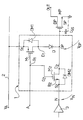
- the drawing shows a schematical view of a holding circuit according to this invention.
- the numeral 1 comprehensively and schematically designates a circuit for holding a field-effect power transistor MP of the MOS (Metal-Oxide Semiconductor) type in a conduction stated on the occurrence of a power outage.
- MOS Metal-Oxide Semiconductor
- That transistor MP is of the n-channel type and conventionally includes a source terminal SP connected to ground, and a drain terminal DP which forms an output terminal OUT for the circuit 1 and intended for connection to an external load, such as an electric motor not shown because of conventional design.
- the power transistor MP further includes a gate terminal GP having an inherent gate capacitance CGS.
- the circuit 1 is connected to an electric power supply line 2, in turn connected to a positive supply pole VA.
- the circuit 1 comprises a first transistor M1 of the p-channel MOS type having its source terminal S1 connected to the line 2, and its drain terminal D1 connected to the gate GP of the transistor MP via a diode D.
- the transistor M1 further includes an intrinsic diode DM1 connected between the drain D1 and the source S1, as well as a gate terminal C1 connected to an input terminal A of the circuit 1 and intended for receiving a signal commanding the make state of the transistor MP.
- a second transistor M2 of the n-channel MOS type be arranged to have its gate terminal G2 connected to the gate G1 of the transistor M1 and its drain terminal D2 connected to the gate GP of the power transistor MP.
- That second transistor M2 also has the source S2 and substrate B2 terminals connected to each other and and to an input terminal IN which is connected to the output of a driver circuit 3 external of the circuit 1 and operative to drive the transistor MP.
- the transistor M2 is in turn provided with an intrinsic diode DM2 connected between the source S2 and drain D2 terminals; in addition, the transistor M2 should be sized to have a negligible serial resistance compared to the serial resistance of the driver 3.
- the circuit 1 of this invention operates as follows.
- the transistor M2 is instead conducting if the supply voltage VA is higher than the voltage VIN at the input terminal IN plus the threshold voltage VTH2 of the transistor M2. Even if the threshold voltage VTH2 is greater than a diode voltage drop, the driver 3 would drive the gate GP of the transistor MP and all the output voltage VIN is delivered to that gate less the voltage drop across the intrinsic diode DM2.
- the transistor M2 is in an off state in that there is a positive or zero voltage VIN at the source and zero voltage at the gate G2.
- the transistor M2 is still in a non-conducting state, and the transistor M1 could provide a route for discharging the capacitor CGS of the power transistor through the diode DM1. Actually, since the voltage VA is lower than the voltage VGP at the gate of the transistor MP, the diode D would be reverse biased and inhibit discharge of the gate capacitor of the power transistor MP.
- diode D isolates a current leakout through transistor M1, having the intrinsic diode DM1, and transistor M2 is off and isolates the driver 3 from the gate capacitor of the power transistor. Accordingly, on the occurrence of the supply voltage VA drop, the gate of the power transistor is automatically isolated from all the components of the circuit 1, and holds that transistor in a permanently conducting state.
- the circuit of this invention solves, therefore, the technical problem and affords a number of advantages, an outstanding one being that the very inherent gate capacitance of the power transistor is utilized to hold it in conduction on the occurrence of a drop in the voltage supply.
- the circuit of this invention is made up of peculiarly low number of components, and makes provisions unnecessary to cancel leakage currents of the drivers in the absence of power supply.
- the circuit can be driven, in the absence of power supply, in an extremely simple way, since the input impedance of the make terminal A is almost infinite and it receives under that condition a signal having a low logic value.
Landscapes
- Electronic Switches (AREA)
- Protection Of Generators And Motors (AREA)
- Power Conversion In General (AREA)
Claims (1)
- Eine Schaltung (1) zum Halten eines MOS-Leistungstransistors (MP) in einem leitfähigen Zustand bei Auftreten eines Ausfalles der Versorgungsspannung (VA), mit einem ersten p-Kanal-MOS-Transistor (M1), der mit seiner Source (S1) an einen ersten Anschluß (2) der Versorgungsspannung (VA), mit seinem Drain (D1) an das Gate (GP) des Leistungstransistors (MP) und mit seinem Gate (G1) an einen ersten Eingangsanschluß (A) angeschlossen ist und der wirksam ist, um das Gate (GP) des Leistungstransistors (MP) mit dem ersten Anschluß (2) der Spannungsversorgung wirkungsmäßig zu verbinden, wenn er durch ein Signal, das an den ersten Eingangsanschluß (A) angelegt wird, in einen leitfähigen Zustand gebracht wird, wobei der Leistungstransistor (MP) mit seinem Gate (GP) an einen zweiten Eingangsanschluß (IN) zum Empfangen von Treibersignalen angeschlossen ist, mit seiner Source (SP) an einen zweiten Anschluß der Spannungsversorgung und mit seinem Drain (DP) an eine Last angeschlossen ist, wobei die Schaltung (1) dadurch gekennzeichnet ist, daß sie eine Diode (D), die in einer vorwärts vorgespannten Richtung zwischen dem Drain (D1) des ersten Transistors (M1) und dem Gate (GP) des Leistungstransistors geschaltet ist, und einen zweiten Transistor (M2) des MOS-Types umfaßt, dessen Gate (G2) mit dem Gate (G1) des ersten Transistors (M1), dessen Drain mit dem Gate (GP) des Leistungstransistors (MP) und dessen Source (S2) mit dem zweiten Eingangsanschluß (IN) verbunden ist und der durch das an den ersten Eingangsanschluß (A) angelegte Signal derart betätigbar ist, daß er nicht-leitfähig ist.
Applications Claiming Priority (2)
| Application Number | Priority Date | Filing Date | Title |
|---|---|---|---|
| IT8723162A IT1224644B (it) | 1987-12-22 | 1987-12-22 | Circuito per il mantenimento in conduzione di un transistore mos in mancanza di tensione di alimentazione elettrica. |
| IT2316287 | 1987-12-22 |
Publications (3)
| Publication Number | Publication Date |
|---|---|
| EP0321702A2 EP0321702A2 (de) | 1989-06-28 |
| EP0321702A3 EP0321702A3 (en) | 1990-08-22 |
| EP0321702B1 true EP0321702B1 (de) | 1993-10-13 |
Family
ID=11204432
Family Applications (1)
| Application Number | Title | Priority Date | Filing Date |
|---|---|---|---|
| EP88119207A Expired - Lifetime EP0321702B1 (de) | 1987-12-22 | 1988-11-18 | Schaltung, um einen MOS-Transistor bei Ausfall der Versorgungsspannung im leitenden Zustand zu halten |
Country Status (5)
| Country | Link |
|---|---|
| US (1) | US4914316A (de) |
| EP (1) | EP0321702B1 (de) |
| JP (1) | JP2770969B2 (de) |
| DE (1) | DE3884925T2 (de) |
| IT (1) | IT1224644B (de) |
Families Citing this family (11)
| Publication number | Priority date | Publication date | Assignee | Title |
|---|---|---|---|---|
| US5065047A (en) * | 1989-03-27 | 1991-11-12 | Nissan Motor Co., Ltd. | Digital circuit including fail-safe circuit |
| US5148047A (en) * | 1990-06-11 | 1992-09-15 | Motorola, Inc. | CMOS bus driver circuit with improved speed |
| US5138186A (en) * | 1990-07-13 | 1992-08-11 | Illinois Tool Works Inc. | Solid state switch with last state memory |
| US5130562A (en) * | 1990-08-31 | 1992-07-14 | Advanced Micro Devices, Inc. | Integrated power-sense circuit |
| US6031408A (en) * | 1991-09-20 | 2000-02-29 | Motorola, Inc. | Square-law clamping circuit |
| JP3545049B2 (ja) * | 1993-06-22 | 2004-07-21 | エスティーマイクロエレクトロニクス,インコーポレイテッド | 電源エネルギ障害時の逆起電力整流電圧 |
| JPH07129538A (ja) * | 1993-10-29 | 1995-05-19 | Mitsubishi Denki Semiconductor Software Kk | 半導体集積回路 |
| DE69328623T2 (de) * | 1993-11-30 | 2001-02-08 | Stmicroelectronics S.R.L., Agrate Brianza | Stabile Referenzspannungsgeneratorschaltung |
| FR2738422B1 (fr) * | 1995-08-31 | 1997-10-24 | Suisse Electronique Microtech | Circuit de polarisation destine a fixer le niveau moyen d'une tension alternative |
| US6509781B2 (en) * | 2001-03-20 | 2003-01-21 | Koninklijke Philips Electronics N.V. | Circuit and method for controlling a dynamic, bi-directional high voltage analog switch |
| EP1415398A2 (de) * | 2001-07-25 | 2004-05-06 | Koninklijke Philips Electronics N.V. | Ausgangstreiber mit ausgangsstrommesswiderstand |
Citations (2)
| Publication number | Priority date | Publication date | Assignee | Title |
|---|---|---|---|---|
| EP0236967A1 (de) * | 1986-03-11 | 1987-09-16 | Siemens Aktiengesellschaft | Schaltungsanordnung zum Ansteuern eines mit sourceseitiger Last verbundenen Mosfet |
| EP0246361A2 (de) * | 1986-04-24 | 1987-11-25 | Robert Bosch Gmbh | Aus einem Akkumulator gespeistes und mittels Tastschalter ein- und ausschaltbares elektronisches Gerät |
Family Cites Families (5)
| Publication number | Priority date | Publication date | Assignee | Title |
|---|---|---|---|---|
| US3700968A (en) * | 1971-01-20 | 1972-10-24 | Messerschmitt Boelkow Blohm | Electric fuse circuit |
| JPS52153630A (en) * | 1976-06-16 | 1977-12-20 | Matsushita Electric Ind Co Ltd | Semiconductor memory device |
| FR2445642A1 (fr) * | 1978-12-29 | 1980-07-25 | Radiotechnique Compelec | Agencement de securite en cas de chute d'une tension d'alimentation continue |
| US4317056A (en) * | 1980-03-24 | 1982-02-23 | Gte Products Corporation | Voltage monitoring and indicating circuit |
| US4663547A (en) * | 1981-04-24 | 1987-05-05 | General Electric Company | Composite circuit for power semiconductor switching |
-
1987
- 1987-12-22 IT IT8723162A patent/IT1224644B/it active
-
1988
- 1988-11-18 EP EP88119207A patent/EP0321702B1/de not_active Expired - Lifetime
- 1988-11-18 DE DE88119207T patent/DE3884925T2/de not_active Expired - Fee Related
- 1988-12-12 US US07/283,232 patent/US4914316A/en not_active Expired - Lifetime
- 1988-12-22 JP JP63322259A patent/JP2770969B2/ja not_active Expired - Fee Related
Patent Citations (2)
| Publication number | Priority date | Publication date | Assignee | Title |
|---|---|---|---|---|
| EP0236967A1 (de) * | 1986-03-11 | 1987-09-16 | Siemens Aktiengesellschaft | Schaltungsanordnung zum Ansteuern eines mit sourceseitiger Last verbundenen Mosfet |
| EP0246361A2 (de) * | 1986-04-24 | 1987-11-25 | Robert Bosch Gmbh | Aus einem Akkumulator gespeistes und mittels Tastschalter ein- und ausschaltbares elektronisches Gerät |
Also Published As
| Publication number | Publication date |
|---|---|
| IT1224644B (it) | 1990-10-18 |
| IT8723162A0 (it) | 1987-12-22 |
| EP0321702A3 (en) | 1990-08-22 |
| US4914316A (en) | 1990-04-03 |
| DE3884925T2 (de) | 1994-02-03 |
| JP2770969B2 (ja) | 1998-07-02 |
| DE3884925D1 (de) | 1993-11-18 |
| JPH024007A (ja) | 1990-01-09 |
| EP0321702A2 (de) | 1989-06-28 |
Similar Documents
| Publication | Publication Date | Title |
|---|---|---|
| US4736121A (en) | Charge pump circuit for driving N-channel MOS transistors | |
| US10840898B2 (en) | Semiconductor device and electronic control device | |
| EP2071724B1 (de) | Netzteilsteuerschaltung | |
| EP2071725B1 (de) | Stromversorgungssteuerschaltung | |
| US20040217653A1 (en) | Supply selection circuit with programmable hysteresis | |
| EP0321702B1 (de) | Schaltung, um einen MOS-Transistor bei Ausfall der Versorgungsspannung im leitenden Zustand zu halten | |
| EP2442446A2 (de) | Hochspannungsausgangstreiber | |
| EP1709741B1 (de) | Mos-schaltnetzwerk | |
| US5391948A (en) | Surge-resistant protection circuit for vehicle | |
| US5057720A (en) | Output buffering H-bridge circuit | |
| US20210351177A1 (en) | Semiconductor device | |
| US5280201A (en) | Semiconductor logic circuit apparatus | |
| US5034875A (en) | Voltage multiplier circuit | |
| EP1183780B1 (de) | Elektronische schaltung mit einem digitalen treiber zum treiben einer kapazitiven last | |
| US5959494A (en) | High-voltage switch control | |
| US4795917A (en) | Low power high voltage driver circuit | |
| US12113524B2 (en) | Active bootstrapping drivers | |
| US6175256B1 (en) | Control circuit | |
| US20230014972A1 (en) | Driving apparatus | |
| US7319359B2 (en) | High current charge pump for intelligent power switch drive | |
| EP0533354A1 (de) | Treiberschaltung | |
| CN114184924B (zh) | 集成电路和半导体装置 | |
| CN115021537B (zh) | 一种预驱动电路 | |
| JPH0770981B2 (ja) | パワーmosスイッチ | |
| JP2005304268A (ja) | 負荷駆動回路 |
Legal Events
| Date | Code | Title | Description |
|---|---|---|---|
| PUAI | Public reference made under article 153(3) epc to a published international application that has entered the european phase |
Free format text: ORIGINAL CODE: 0009012 |
|
| AK | Designated contracting states |
Kind code of ref document: A2 Designated state(s): DE FR GB NL SE |
|
| PUAL | Search report despatched |
Free format text: ORIGINAL CODE: 0009013 |
|
| AK | Designated contracting states |
Kind code of ref document: A3 Designated state(s): DE FR GB NL SE |
|
| 17P | Request for examination filed |
Effective date: 19900926 |
|
| 17Q | First examination report despatched |
Effective date: 19920225 |
|
| GRAA | (expected) grant |
Free format text: ORIGINAL CODE: 0009210 |
|
| AK | Designated contracting states |
Kind code of ref document: B1 Designated state(s): DE FR GB NL SE |
|
| REF | Corresponds to: |
Ref document number: 3884925 Country of ref document: DE Date of ref document: 19931118 |
|
| ET | Fr: translation filed | ||
| PLBE | No opposition filed within time limit |
Free format text: ORIGINAL CODE: 0009261 |
|
| STAA | Information on the status of an ep patent application or granted ep patent |
Free format text: STATUS: NO OPPOSITION FILED WITHIN TIME LIMIT |
|
| 26N | No opposition filed | ||
| EAL | Se: european patent in force in sweden |
Ref document number: 88119207.4 |
|
| REG | Reference to a national code |
Ref country code: FR Ref legal event code: D6 |
|
| PGFP | Annual fee paid to national office [announced via postgrant information from national office to epo] |
Ref country code: SE Payment date: 20011106 Year of fee payment: 14 |
|
| PGFP | Annual fee paid to national office [announced via postgrant information from national office to epo] |
Ref country code: NL Payment date: 20011129 Year of fee payment: 14 |
|
| REG | Reference to a national code |
Ref country code: GB Ref legal event code: IF02 |
|
| PGFP | Annual fee paid to national office [announced via postgrant information from national office to epo] |
Ref country code: FR Payment date: 20021108 Year of fee payment: 15 |
|
| PGFP | Annual fee paid to national office [announced via postgrant information from national office to epo] |
Ref country code: GB Payment date: 20021113 Year of fee payment: 15 |
|
| PG25 | Lapsed in a contracting state [announced via postgrant information from national office to epo] |
Ref country code: SE Free format text: LAPSE BECAUSE OF NON-PAYMENT OF DUE FEES Effective date: 20021119 |
|
| PGFP | Annual fee paid to national office [announced via postgrant information from national office to epo] |
Ref country code: DE Payment date: 20021121 Year of fee payment: 15 |
|
| PG25 | Lapsed in a contracting state [announced via postgrant information from national office to epo] |
Ref country code: NL Free format text: LAPSE BECAUSE OF NON-PAYMENT OF DUE FEES Effective date: 20030601 |
|
| EUG | Se: european patent has lapsed | ||
| NLV4 | Nl: lapsed or anulled due to non-payment of the annual fee |
Effective date: 20030601 |
|
| PG25 | Lapsed in a contracting state [announced via postgrant information from national office to epo] |
Ref country code: GB Free format text: LAPSE BECAUSE OF NON-PAYMENT OF DUE FEES Effective date: 20031118 |
|
| PG25 | Lapsed in a contracting state [announced via postgrant information from national office to epo] |
Ref country code: DE Free format text: LAPSE BECAUSE OF NON-PAYMENT OF DUE FEES Effective date: 20040602 |
|
| GBPC | Gb: european patent ceased through non-payment of renewal fee |
Effective date: 20031118 |
|
| PG25 | Lapsed in a contracting state [announced via postgrant information from national office to epo] |
Ref country code: FR Free format text: LAPSE BECAUSE OF NON-PAYMENT OF DUE FEES Effective date: 20040730 |
|
| REG | Reference to a national code |
Ref country code: FR Ref legal event code: ST |