EP0321240A2 - Method and apparatus for interrupt processing - Google Patents
Method and apparatus for interrupt processing Download PDFInfo
- Publication number
- EP0321240A2 EP0321240A2 EP88311870A EP88311870A EP0321240A2 EP 0321240 A2 EP0321240 A2 EP 0321240A2 EP 88311870 A EP88311870 A EP 88311870A EP 88311870 A EP88311870 A EP 88311870A EP 0321240 A2 EP0321240 A2 EP 0321240A2
- Authority
- EP
- European Patent Office
- Prior art keywords
- signal
- central processing
- cpu
- processing unit
- interrupt
- Prior art date
- Legal status (The legal status is an assumption and is not a legal conclusion. Google has not performed a legal analysis and makes no representation as to the accuracy of the status listed.)
- Granted
Links
Images


Classifications
-
- G—PHYSICS
- G06—COMPUTING OR CALCULATING; COUNTING
- G06F—ELECTRIC DIGITAL DATA PROCESSING
- G06F13/00—Interconnection of, or transfer of information or other signals between, memories, input/output devices or central processing units
- G06F13/14—Handling requests for interconnection or transfer
- G06F13/20—Handling requests for interconnection or transfer for access to input/output bus
- G06F13/24—Handling requests for interconnection or transfer for access to input/output bus using interrupt
Definitions
- the present invention relates to a processing method and a processing apparatus for a computer system, more particularly, to an interrupt processing method and an interrupt processing apparatus for a computer system having a central processing unit and a plurality of peripheral units (peripheral equipment), wherein an interrupt request signal is transferred from each peripheral unit to the central processing unit, and an interrupt acknowledge signal in response to the interrupt request signal is successively propagated from the central processing unit to each peripheral unit by a daisy chain connection.
- the present invention also relates to an interrupt controller.
- interrupt processing is carried out, for example, by using a daisy chain connection constructed by a plurality of peripheral units.
- An interrupt request signal is output from each peripheral unit to a central processing unit through a signal conductor, and when the central processing unit receives the interrupt request signal and an interrupt processing is enabled, the central processing unit outputs an interrupt acknowledge signal to the peripheral unit by using a daisy chain connection.
- the central processing unit first outputs the interrupt acknowledge signal to a first step peripheral unit, and if the first step peripheral unit does not output the interrupt request signal, the interrupt acknowledge signal is propagated to a second step peripheral unit, i.e., a next step peripheral unit. Therefore, as described above, the interrupt acknowledge signal is successively propagated to each peripheral unit.
- the specific peripheral unit When the interrupt acknowledge signal is propagated to the specific peripheral unit which has output the interrupt request signal, the specific peripheral unit outputs a vector address to the central processing unit through a data bus, so that an interrupt processing routine for the specific peripheral unit is started.
- the above peripheral units may be not only input-output devices or auxiliary storages, but also interrupt controllers.
- the input-output device or auxiliary storage is, for example, a cathode ray tube display, an optical mark reader, and a hard disk drive device, etc.
- the interrupt controller which is used as an interrupt handler or an interrupt generator, controls a plurality of input-output devices or auxiliary storages.
- the central processing unit outputs an error interrupt acknowledge signal, without receiving a correct interrupt request signal. Therefore, none of the peripheral units outputs a response signal to the central processing unit, and thus the central processing unit is held in a response waiting state and the processing is unnecessarily delayed.
- a processing method for a computer system having a central processing unit and a plurality of peripheral units, wherein a request signal is transferred from each peripheral unit to the central processing unit, and an acknowledge signal in response to the request signal is successively propagated from the central processing unit to each peripheral unit by a daisy chain connection, which comprises: a step for setting indicative information to an end indicative information storing means of at least one of the peripheral units; a step for outputting a specific signal notifying the central processing unit of a chain end state, from the peripheral unit at which the indicative information is set to the end indicative information storing means thereof, when the peripheral unit receives the acknowledge signal and does not output the request signal; and a step for returning the central processing unit from a response waiting state by receiving a specific signal.
- a processing apparatus having a central processing unit and a plurality of peripheral units, wherein a request signal is transferred from each of said plurality of peripheral units to said central processing unit, and an acknowledge signal in response to said request signal is successively propagated from said central processing unit to each of said plurality of peripheral units by a daisy chain connection, wherein each of said plurality of peripheral units comprises a request signal output means and input-output terminals, at least one peripheral unit of said plurality of peripheral units comprising an end indicative information storing means storing end indicative information indicative of the end of the daisy chain, and a chain end state notification means, and said central processing unit comprising means of returning from said chain end state; said chain end state notification means being operatively connected to said central processing unit and arranged to notify said central processing unit of a chain end state, when said peripheral unit receives said acknowledge signal and does not output said request signal and when said end indicative information is set in the end indicative information storing means thereof.
- an interrupt controller comprising: an interrupt request signal output means, operatively connected to a central processing unit, for outputting an interrupt request signal to said central processing unit; input-output terminals, operatively connected to said central processing unit or a neighbour interrupt controller, for constructing a daisy chain connection, an end indicative information storing means for storing end indicative information of said daisy chain; and a chain end state notification means, operatively connected to said central processing unit and said end indicative information storing means, for notifying a chain end state to said central processing unit, when an interrupt acknowledge signal output from said central processing unit is propagated to said interrupt controller, said end indicative information being set in said end indicative information means thereof and said interrupt request signal being not output, so that said central processing unit is returned from said response waiting state by receiving a chain end state notification from said chain end state notification means.
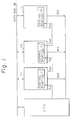
- FIG. 1 is a block diagram illustrating an example of a proposed interrupt processing apparatus.
- reference CPU denotes a central processing unit
- U1 - U n denote peripheral units
- DB denotes a data bus
- IRR denotes a interrupt request signal
- D in denotes an interrupt acknowledge signal from the central processing unit or an immediately prior step
- D out denotes an interrupt acknowledge signal to be output to a next step
- C1′ C n ′ denote control portions.
- an interrupt request signal IRR of each peripheral unit U1 - U n is output to a central processing unit CPU through a common signal conductor.
- the central processing unit CPU receives the interrupt request signal IRR and an interrupt processing is enabled, and the central processing unit CPU outputs an interrupt acknowledge signal D in .
- a control portion C1′ of the peripheral unit U1 receives the interrupt acknowledge signal D in and outputs an interrupt acknowledge signal D out to the next peripheral unit U2 as an interrupt acknowledge signal D in thereof, since the peripheral unit U1 has not output an interrupt request signal.
- the interrupt acknowledge signal is successively propagated to each peripheral unit.
- a control portion C n ′ of the peripheral unit U n When the interrupt acknowledge signal D in is propagated to the peripheral unit U n which has output an interrupt request signal IRR, a control portion C n ′ of the peripheral unit U n outputs a vector address to the central processing unit CPU through a data bus DB, and thus an interrupt processing routine for the peripheral unit U n is started.
- Fig. 1 when noise exists in a signal conductor in which the interrupt request signal IRR is propagated, the noise may be taken as the interrupt request signal IRR in the central processing unit CPU.
- the central processing unit CPU outputs an interrupt acknowledge signal D in , but none of the peripheral units U1 - U n outputs a response signal to the central processing unit CPU. Therefore, an interrupt acknowledge signal D in is propagated to the final step peripheral unit U n but the central processing unit CPU does not receive a vector address of an interrupt processing routine, and therefore, the central processing unit CPU is held in a response waiting state and a long and unnecessary delay occurs.
- a timer is provided, and when the response waiting state of the central processing unit CPU continues for longer than a specific time, the central processing unit CPU is returned to the normal state from the response waiting state. In this case, however, if the time elapsed is not sufficient, an obstacle is formed by a normal operating state, and therefore, the time elapsed is too long, and thus an unnecessary delay occurs.
- the present invention may reduce a time elapsed before a return from a response waiting state of a central processing unit without a long and unnecessary delay, when an error interrupt request signal is to be propagated to the central processing unit.
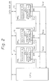
- FIG. 2 is a block diagram illustrating an embodiment of an interrupt processing apparatus according to the present invention.
- reference R1 - R n denote registers
- C1 - C n denote control portions
- SET denotes an end indicative information
- IRR1 - IRR n denote an interrupt request signal generated from each peripheral unit U1 - U n
- D end denotes an end notice signal.
- the peripheral units U1 - U n are input-output devices or auxiliary storages, i.e., each peripheral unit U1 - U n is, for example, a cathode ray tube display, an optical mark reader, and a hard disk drive device, etc. Note, the same portions of Figs.
- Each register R1 - R n is a one-bit register and stores an end indicative information corresponding to one kind of flag.
- the end indicative information is output from a central processing unit CPU to an optional one of the peripheral units through a data bus DB and is set to a register of the one of the peripheral units.
- an interrupt request signal IRR is not output from the peripheral unit U2 and an end indicative information is not set to a register R2 of the control portion C2 , so that an interrupt acknowledge signal D out is transferred to the next control portion of the next step peripheral unit through the control portion C2.
- an interrupt acknowledge signal D out is successively transferred to a control portion C n of the peripheral unit U n as an interrupt acknowledge signal D in thereof, in the same manner.
- an end indicative information is set to the register R n of the peripheral unit U n but an interrupt request IRR n is not received, i.e., an end indicative information SET is output from the register R n to the control portion C n but an interrupt request IRR is not output to the central processing unit CPU, so that a one-bit end notice signal D end is output from the control portion C n to the central processing unit CPU through a signal conductor.
- the central processing unit CPU receives the end notice signal D end and confirms a chain end state, and then the central processing unit CPU is returned from a response waiting state and carries out a predetermined error processing, etc.
- the end indicative information is set to the final step of the daisy chain connection .
- the end indicative information is set to an optional step peripheral unit within the daisy chain connection, an end portion of the daisy chain connection can be determined by the optional step peripheral unit. This is preferable since the interrupt requests output from low priority peripheral units connected to the daisy chain connection are disregarded, and a specific processing is carried out on a temporary basis.
- registers R1 - R n are provided for all peripheral units U1 - U n , but a register can be provided at only one of the peripheral units U1 - U n ; for example, only the register R n and the control portion C n as described above can be provided at the final peripheral unit.
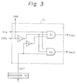
- FIG. 3 is a circuit diagram of an example of a control portion shown in Fig. 2.
- the control portion C1 comprises two inverter circuits I1 , I2 and two three-input AND gate circuits G1 , G2.
- An input terminal of the inverter circuit I1 is connected to an interrupt request output unit (not shown) included in each peripheral unit and receives an interrupt request signal IRR1.
- the interrupt request output unit is a signal output means or a signal output function in the peripheral unit, and a reference IRR substantially denotes the same signal as the interrupt request signal IRR1.
- An input terminal of the inverter circuit I2 is connected to the register R1 and receives an end indicative signal SET from the register R1.
- a first input of the AND gate circuits G1 is connected to the central processing unit CPU and receives an interrupt acknowledge signal D in .
- the AND gate circuit G1 is provided for a post control portion of the first step peripheral unit U1
- the first input of the AND gate circuit G1 is connected to a control portion of an immediately prior peripheral unit, for example, the AND gate circuit G1 is provided for the control portion C2 of the second step peripheral unit U2 and the first input of the AND gate circuits G1 is connected to an immediately prior control portion C1.
- a second input of the AND gate circuits G1 is connected to the first inverter circuit I1 and receives an inverted signal of the interrupt request signal IRR, a third input thereof is connected to the second inverter circuit I2 and receives an inverted signal of the end indicative signal SET, and an output thereof is connected to an immediately adjacent equipment, i.e., a second peripheral unit U2 , and outputs an interrupt acknowledge signal D out to the second peripheral unit U2.
- the AND gate circuits G1 is provided for a control portion C n of the final step peripheral unit U n , the output of the AND gate circuit G1 is not connected.
- a first input of the AND gate circuit G2 is connected to the first input of the AND gate circuit G1 and receives the interrupt acknowledge signal D in .
- the AND gate circuits G2 is provided for a post control portion of the first step peripheral unit U1
- the first input of the AND gate circuit G2 is connected to a control portion of an immediately prior peripheral unit, as for the AND gate circuit G1.
- a second input of the AND gate circuit G2 is connected to the second input of the AND gate circuit G1 and receives the inverted signal of the interrupt request signal IRR, a third input thereof is connected to the register R1 and receives the end indicative signal SET, and an output thereof is connected to the central processing unit CPU and transfers an end notice signal D end to the central processing unit CPU through a signal conductor.
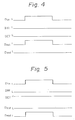
- a line of 1 corresponds to a state of Fig. 4 (a timing chart when not setting a register)
- a line of 2 corresponds to a state of Fig. 5 (a timing chart when setting a register).
- the line 2 of the truth table indicates that the interrupt acknowledge signal D in is "1" when the end indicative signal SET is "0", i.e., an end of the daisy chain is indicated, and the interrupt request signal IRR is also "0".
- the interrupt acknowledge signal D out is brought to "0”
- the interrupt acknowledge signal D in is not transferred to the next step, but the end notice signal D end is brought to "1” and the central processing unit CPU is notified of a chain end state.
- the central processing unit CPU rapidly returns from the response waiting state, and carries out a specific error processing, etc.
- the interrupt request signal IRR is "1", i.e., the interrupt request is output from the peripheral unit by itself, the interrupt acknowledge signal D in is not transferred to the next step, and the end notice signal D end is maintained at "0". Therefore, a vector address is output from the peripheral unit to the central processing unit CPU, so that an interrupt processing routine is carried out.
- FIG. 6 is a block diagram illustrating another embodiment of an interrupt processing apparatus according to the present invention.
- This embodiment corresponds to the embodiment of Fig. 2, and the same portions and same signals shown in Figs. 2 and 6 are indicated by the same references.
- the difference between these two embodiments is a propagation of the end notice signal D end .
- the end notice signal D end from each peripheral unit is transferred to the central processing unit CPU through an exclusive signal conductor, and the central processing unit is returned from the response waiting state to a normal state.
- an end notice signal D end is transferred through a data bus DB, for example, which end notice signal D end is a signal indicating a vector address of an error processing subroutine.
- the central processing unit CPU When the central processing unit CPU receives the vector address signal D end , the central processing unit CPU is returned from the response waiting state and the error processing subroutine corresponding to the vector address signal D end is carried out.
- the exclusive signal conductor for transferring the end notice signal D end from each peripheral unit to the central processing unit CPU can be omitted.
- FIG. 7 is a block diagram of an interrupt processing apparatus using interrupt controllers.
- each peripheral unit U1 - U n comprises an input-output device or an auxiliary storage, for example, a cathode ray tube display, an optical mark reader, and a hard disk drive device, etc., but in the interrupt processing apparatus of Fig. 7, each peripheral unit U1 - U n comprises an interrupt controller. Note, in Fig. 7, only three peripheral units U1 - U3 are indicated.
- the interrupt controller which is used as an interrupt handler or an interrupt generator, controls a plurality of, for example, seven, input-output devices or auxiliary storages.
- the peripheral unit U1 is used as an interrupt handler by applying a power supply potential to a function select terminal FSEL of an interrupt controller
- each peripheral unit U2 and U3 is used as an interrupt generator by applying an earth potential to a function select terminal FSEL of an interrupt controller.
- seven input-output devices (or auxiliary storages) IOD0 - IOD6 are connected to each interrupt handler or interrupt generator U1 - U3 through I/O ports respectively.
- the seven input-output devices IOD0 - IOD6 output a local interrupt request signal LIR0# - LIR6# to each peripheral unit U1 - U3 of an interrupt handler or an interrupt generator, respectively.
- Each peripheral unit U1 - U3 outputs local interrupt acknowledge signals LIK0 - LIK2 and local interrupt acknowledge strobe signal LIKSTB# to each decoder DE1 - DE3 , and each decoder DE1 - DE3 outputs an interrupt acknowledge signal to each input-output device IOD0 - IOD6 , respectively.
- the peripheral unit of the interrupt handler U1 is controlled by the central processing unit CPU through an address bus (A1 - 5), a data bus (D24 - 31), and a control bus.
- the peripheral unit U1 is connected to the central processing unit CPU by interrupt request signal conductors IRL0 - IRL2, and an interrupt request signal from the peripheral unit U1 is transferred to the central processing unit CPU and an interrupt acknowledge signal ACKIN# from the central processing unit is transferred to the peripheral unit U1 , through the system bus.
- the peripheral units of the interrupt generators U2 , U3 are controlled by the central processing unit CPU by an address bus (A1 - 5), a data bus (D24 - 31), and a control bus, through a system bus.
- peripheral units U2 , U3 output bus interrupt signals BIR0# - BIR6# to the peripheral unit U1 through the system bus, and an interrupt acknowledge signal ACKOUT# of the peripheral unit U1 is transferred to the peripheral unit U2 as an interrupt acknowledge signal ACKIN# and an interrupt acknowledge signal ACKOUT# of the peripheral unit U2 is transferred to the peripheral unit U3 , respectively.
- reference # indicates an inverted signal.
- Figure 8 is a block diagram illustrating an example of an interrupt controller applied to the interrupt processing apparatus shown in Fig. 2.
- reference IR denotes an interrupt control portion
- reference ir denotes an interrupt request from a plurality of peripheral units. Note the same portions as shown in Figs. 2 and 8 are indicated by same reference.
- An interrupt controller which is used as an interrupt handler or an interrupt generator of the peripheral units U1 - U n in Fig. 2, comprises an interrupt control portion IR which groups the interrupt requests output from a plurality of, for example, seven input-output devices or auxiliary storages, on a priority basis, and controls a ranking of the interrupt requests.
- the interrupt control portion IR is connected to the central processing unit CPU through a data bus DB, and outputs a vector address corresponding to the peripheral unit outputting the interrupt request, when the interrupt control portion IR receives the interrupt acknowledge signal D in .
- a setting processing for setting the end indicative information to the register R1 is also carried out through the data bus DB and the interrupt control portion IR.
- a daisy chain connection is constructed by using interrupt controllers IRC as described in Fig. 7, and thus an optional portion of the daisy chain connection by software can be omitted.
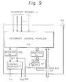
- Figure 9 is block diagram illustrating an example of an interrupt controller applied to the interrupt processing apparatus shown in Fig. 3.
- reference IR denotes an interrupt control portion
- reference ir denotes an interrupt request from a plurality of input-output devices or auxiliary storages. Note, the same portions as shown in Figs. 3 and 9 are indicated by same references.
- the end notice signal D end is transferred to the central processing unit by a one-bit signal conductor, but as shown in Fig. 9, a vector address for starting an error processing subroutine can be transferred, instead of the end notice signal D end , to the central processing unit CPU through the data bus DB.
- the difference of the configurations of the interrupt controllers of Figs. 8 and 9 is that a register RV which sets a vector address for error processing and a three state buffer BF are provided, and the three states buffer is controlled by the end notice signal D end .
- An operation of a control portion C1 is same as that of Figs. 2 and 8.
- the vector address for error processing is previously set through the data bus DB by the central processing unit CPU.
- the three states buffer BF When the end notice signal D end is "0", the three states buffer BF is disabled and an output of the three states buffer BF is brought to a high impedance state. When the end notice signal D end is "1”, the three states buffer BF is enabled and the vector address stored in the register RV is output to the central processing unit CPU through the data bus DB.
- a delay for the central processing unit CPU is reduced.
- a daisy chain connection may be cut at an optional portion and an interrupt request from an irrelevant peripheral unit can be ignored so that the efficiency of the processing is improved.
Landscapes
- Engineering & Computer Science (AREA)
- Theoretical Computer Science (AREA)
- Physics & Mathematics (AREA)
- General Engineering & Computer Science (AREA)
- General Physics & Mathematics (AREA)
- Bus Control (AREA)
Abstract
Description
- The present invention relates to a processing method and a processing apparatus for a computer system, more particularly, to an interrupt processing method and an interrupt processing apparatus for a computer system having a central processing unit and a plurality of peripheral units (peripheral equipment), wherein an interrupt request signal is transferred from each peripheral unit to the central processing unit, and an interrupt acknowledge signal in response to the interrupt request signal is successively propagated from the central processing unit to each peripheral unit by a daisy chain connection. The present invention also relates to an interrupt controller.
- At present, interrupt processing is carried out, for example, by using a daisy chain connection constructed by a plurality of peripheral units. An interrupt request signal is output from each peripheral unit to a central processing unit through a signal conductor, and when the central processing unit receives the interrupt request signal and an interrupt processing is enabled, the central processing unit outputs an interrupt acknowledge signal to the peripheral unit by using a daisy chain connection. Namely, the central processing unit first outputs the interrupt acknowledge signal to a first step peripheral unit, and if the first step peripheral unit does not output the interrupt request signal, the interrupt acknowledge signal is propagated to a second step peripheral unit, i.e., a next step peripheral unit. Therefore, as described above, the interrupt acknowledge signal is successively propagated to each peripheral unit. When the interrupt acknowledge signal is propagated to the specific peripheral unit which has output the interrupt request signal, the specific peripheral unit outputs a vector address to the central processing unit through a data bus, so that an interrupt processing routine for the specific peripheral unit is started. Note, the above peripheral units may be not only input-output devices or auxiliary storages, but also interrupt controllers. The input-output device or auxiliary storage is, for example, a cathode ray tube display, an optical mark reader, and a hard disk drive device, etc. The interrupt controller, which is used as an interrupt handler or an interrupt generator, controls a plurality of input-output devices or auxiliary storages.
- Note, if noise exists in the signal conductor in which the interrupt request signal is transferred, this noise may be taken as the interrupt request signal by the central processing unit. In this case, the central processing unit outputs an error interrupt acknowledge signal, without receiving a correct interrupt request signal. Therefore, none of the peripheral units outputs a response signal to the central processing unit, and thus the central processing unit is held in a response waiting state and the processing is unnecessarily delayed.
- In consideration of the above-mentioned problems when an error interrupt request signal is propagated to a central processing unit, it is desirable to reduce a delay in a return from a response waiting state of the central processing unit, to avoid an unnecessary waste of time.
- According to one aspect of the present invention, there is provided a processing method for a computer system having a central processing unit and a plurality of peripheral units, wherein a request signal is transferred from each peripheral unit to the central processing unit, and an acknowledge signal in response to the request signal is successively propagated from the central processing unit to each peripheral unit by a daisy chain connection, which comprises: a step for setting indicative information to an end indicative information storing means of at least one of the peripheral units; a step for outputting a specific signal notifying the central processing unit of a chain end state, from the peripheral unit at which the indicative information is set to the end indicative information storing means thereof, when the peripheral unit receives the acknowledge signal and does not output the request signal; and a step for returning the central processing unit from a response waiting state by receiving a specific signal.
- According to a second aspect of the present invention, there is provided a processing apparatus having a central processing unit and a plurality of peripheral units, wherein a request signal is transferred from each of said plurality of peripheral units to said central processing unit, and an acknowledge signal in response to said request signal is successively propagated from said central processing unit to each of said plurality of peripheral units by a daisy chain connection, wherein each of said plurality of peripheral units comprises a request signal output means and input-output terminals, at least one peripheral unit of said plurality of peripheral units comprising an end indicative information storing means storing end indicative information indicative of the end of the daisy chain, and a chain end state notification means, and said central processing unit comprising means of returning from said chain end state;
said chain end state notification means being operatively connected to said central processing unit and arranged to notify said central processing unit of a chain end state, when said peripheral unit receives said acknowledge signal and does not output said request signal and when said end indicative information is set in the end indicative information storing means thereof. - According to a third aspect of the present invention, there is provided an interrupt controller comprising:
an interrupt request signal output means, operatively connected to a central processing unit, for outputting an interrupt request signal to said central processing unit;
input-output terminals, operatively connected to said central processing unit or a neighbour interrupt controller, for constructing a daisy chain connection,
an end indicative information storing means for storing end indicative information of said daisy chain; and
a chain end state notification means, operatively connected to said central processing unit and said end indicative information storing means, for notifying a chain end state to said central processing unit, when an interrupt acknowledge signal output from said central processing unit is propagated to said interrupt controller, said end indicative information being set in said end indicative information means thereof and said interrupt request signal being not output, so that said central processing unit is returned from said response waiting state by receiving a chain end state notification from said chain end state notification means. - The present invention will be more clearly understood from the description of the preferred embodiments as set forth below with reference to the accompanying drawings, wherein:
- Fig.1 is a block diagram illustrating an example of a prior-proposed interrupt processing apparatus;
- Fig.2 is a block diagram illustrating an embodiment of an interrupt processing apparatus according to the present invention;
- Fig.3 is a circuit diagram of an example of a control portion shown in Fig.2;
- Fig.4 is a timing chart of a register shown in Fig.2 when not set;
- Fig.5 is a timing chart of a register shown in Fig.2 when set;
- Fig.6 is a block diagram illustrating another embodiment of an interrupt processing apparatus according to the present invention;
- Fig.7 is a block diagram of an interrupt processing apparatus using interrupt controllers;
- Fig.8 is a block diagram illustrating an example of an interrupt controller applied to the interrupt processing apparatus shown in Fig. 2; and,
- Fig. 9 is a block diagram illustrating an example of an interrupt controller applied to the interrupt processing apparatus shown in Fig. 3.
- For a better understanding of the preferred embodiments, the problems of a prior proposal will be first explained.
- Figure 1 is a block diagram illustrating an example of a proposed interrupt processing apparatus. In this drawing, reference CPU denotes a central processing unit, U₁ - Un denote peripheral units, DB denotes a data bus, IRR denotes a interrupt request signal, Din denotes an interrupt acknowledge signal from the central processing unit or an immediately prior step, Dout denotes an interrupt acknowledge signal to be output to a next step, and C₁′ Cn′ denote control portions.
- In Fig. 1, an interrupt request signal IRR of each peripheral unit U₁ - Un is output to a central processing unit CPU through a common signal conductor. For example, when the peripheral unit Un outputs an interrupt request signal IRR, the central processing unit CPU receives the interrupt request signal IRR and an interrupt processing is enabled, and the central processing unit CPU outputs an interrupt acknowledge signal Din. A control portion C₁′ of the peripheral unit U₁ receives the interrupt acknowledge signal Din and outputs an interrupt acknowledge signal Dout to the next peripheral unit U₂ as an interrupt acknowledge signal Din thereof, since the peripheral unit U₁ has not output an interrupt request signal. Thus, as described above, the interrupt acknowledge signal is successively propagated to each peripheral unit. When the interrupt acknowledge signal Din is propagated to the peripheral unit Un which has output an interrupt request signal IRR, a control portion Cn′ of the peripheral unit Un outputs a vector address to the central processing unit CPU through a data bus DB, and thus an interrupt processing routine for the peripheral unit Un is started.
- In Fig. 1, when noise exists in a signal conductor in which the interrupt request signal IRR is propagated, the noise may be taken as the interrupt request signal IRR in the central processing unit CPU. In this case, the central processing unit CPU outputs an interrupt acknowledge signal Din , but none of the peripheral units U₁ - Un outputs a response signal to the central processing unit CPU. Therefore, an interrupt acknowledge signal Din is propagated to the final step peripheral unit Un but the central processing unit CPU does not receive a vector address of an interrupt processing routine, and therefore, the central processing unit CPU is held in a response waiting state and a long and unnecessary delay occurs.
- To solve the above described problem, a timer is provided, and when the response waiting state of the central processing unit CPU continues for longer than a specific time, the central processing unit CPU is returned to the normal state from the response waiting state. In this case, however, if the time elapsed is not sufficient, an obstacle is formed by a normal operating state, and therefore, the time elapsed is too long, and thus an unnecessary delay occurs.
- In consideration of the above, the present invention may reduce a time elapsed before a return from a response waiting state of a central processing unit without a long and unnecessary delay, when an error interrupt request signal is to be propagated to the central processing unit.
- Below, an interrupt processing method and an interrupt processing apparatus of the present invention will be explained in detail with reference to the drawings.
- Figure 2 is a block diagram illustrating an embodiment of an interrupt processing apparatus according to the present invention. In Fig. 2, reference R₁ - Rn denote registers, C₁ - Cn denote control portions, SET denotes an end indicative information, IRR₁ - IRRn denote an interrupt request signal generated from each peripheral unit U₁ - Un , and Dend denotes an end notice signal. Note, the peripheral units U₁ - Un are input-output devices or auxiliary storages, i.e., each peripheral unit U₁ - Un is, for example, a cathode ray tube display, an optical mark reader, and a hard disk drive device, etc. Note, the same portions of Figs. 1 and 2 are indicated by the same references. An interrupt processing using a daisy chain connection in a normal state, is the same as that of the apparatus of Fig. 1, and thus only the case where an error interrupt request signal is generated by noise, etc., will be explained below.
- Each register R₁ - Rn is a one-bit register and stores an end indicative information corresponding to one kind of flag. The end indicative information is output from a central processing unit CPU to an optional one of the peripheral units through a data bus DB and is set to a register of the one of the peripheral units. For example, assuming that an end indicative information is set to a register Rn of a peripheral unit Un , and none of the peripheral units U₁ - Un generates an interrupt request signal IRR₁ - IRRn , in this state, when the central processing unit takes a noise signal as an interrupt request signal and starts an interrupt acceptance processing, i.e., the central processing unit CPU outputs an interrupt acknowledge signal Din to a control portion C₁ of a first step peripheral unit U₁ , an interrupt request signal IRR is not output from the peripheral unit U₁ and an end indicative information is not set to a register R₁ of the control portion C₁ , so that an interrupt acknowledge signal Dout is transferred to a control portion C₂ of a second step peripheral unit U₂ as an interrupt acknowledge signal Din thereof. Similarly, in the second step peripheral unit U₂ , an interrupt request signal IRR is not output from the peripheral unit U₂ and an end indicative information is not set to a register R₂ of the control portion C₂ , so that an interrupt acknowledge signal Dout is transferred to the next control portion of the next step peripheral unit through the control portion C₂.
- As described above, an interrupt acknowledge signal Dout is successively transferred to a control portion Cn of the peripheral unit Un as an interrupt acknowledge signal Din thereof, in the same manner. In the peripheral unit Un , an end indicative information is set to the register Rn of the peripheral unit Un but an interrupt request IRRn is not received, i.e., an end indicative information SET is output from the register Rn to the control portion Cn but an interrupt request IRR is not output to the central processing unit CPU, so that a one-bit end notice signal Dend is output from the control portion Cn to the central processing unit CPU through a signal conductor. The central processing unit CPU receives the end notice signal Dend and confirms a chain end state, and then the central processing unit CPU is returned from a response waiting state and carries out a predetermined error processing, etc.
- In the above example , the end indicative information is set to the final step of the daisy chain connection . If the end indicative information is set to an optional step peripheral unit within the daisy chain connection, an end portion of the daisy chain connection can be determined by the optional step peripheral unit. This is preferable since the interrupt requests output from low priority peripheral units connected to the daisy chain connection are disregarded, and a specific processing is carried out on a temporary basis. In the above embodiment, registers R₁ - Rn are provided for all peripheral units U₁ - Un , but a register can be provided at only one of the peripheral units U₁ - Un; for example, only the register Rn and the control portion Cn as described above can be provided at the final peripheral unit.
- Figure 3 is a circuit diagram of an example of a control portion shown in Fig. 2. As shown in Fig. 3, the control portion C₁ comprises two inverter circuits I₁ , I₂ and two three-input AND gate circuits G₁ , G₂. An input terminal of the inverter circuit I₁ is connected to an interrupt request output unit (not shown) included in each peripheral unit and receives an interrupt request signal IRR₁. Note, the interrupt request output unit is a signal output means or a signal output function in the peripheral unit, and a reference IRR substantially denotes the same signal as the interrupt request signal IRR₁. An input terminal of the inverter circuit I₂ is connected to the register R₁ and receives an end indicative signal SET from the register R₁.
- A first input of the AND gate circuits G₁ is connected to the central processing unit CPU and receives an interrupt acknowledge signal Din. When the AND gate circuit G₁ is provided for a post control portion of the first step peripheral unit U₁ , the first input of the AND gate circuit G₁ is connected to a control portion of an immediately prior peripheral unit, for example, the AND gate circuit G₁ is provided for the control portion C₂ of the second step peripheral unit U₂ and the first input of the AND gate circuits G₁ is connected to an immediately prior control portion C₁. A second input of the AND gate circuits G₁ is connected to the first inverter circuit I₁ and receives an inverted signal of the interrupt request signal IRR, a third input thereof is connected to the second inverter circuit I₂ and receives an inverted signal of the end indicative signal SET, and an output thereof is connected to an immediately adjacent equipment, i.e., a second peripheral unit U₂ , and outputs an interrupt acknowledge signal Dout to the second peripheral unit U₂. When the AND gate circuits G₁ is provided for a control portion Cn of the final step peripheral unit Un , the output of the AND gate circuit G₁ is not connected.
- A first input of the AND gate circuit G₂ is connected to the first input of the AND gate circuit G₁ and receives the interrupt acknowledge signal Din. When the AND gate circuits G₂ is provided for a post control portion of the first step peripheral unit U₁ , the first input of the AND gate circuit G₂ is connected to a control portion of an immediately prior peripheral unit, as for the AND gate circuit G₁. A second input of the AND gate circuit G₂ is connected to the second input of the AND gate circuit G₁ and receives the inverted signal of the interrupt request signal IRR, a third input thereof is connected to the register R₁ and receives the end indicative signal SET, and an output thereof is connected to the central processing unit CPU and transfers an end notice signal Dend to the central processing unit CPU through a signal conductor.
- The operation of this circuit will be explained with reference to the timing charts of Figs. 4, 5 and the following truth table.
TRUTH TABLE Din IRR SET Dout Dend 0 0 0 0 0 0 0 1 0 0 0 1 0 0 0 0 1 1 0 0 ① 1 0 0 1 0 ② 1 0 1 0 1 ③ 1 1 0 0 0 ④ 1 1 1 0 0 - Note, in Figs. 4 and 5, reference H corresponds to "1", and reference L corresponds to "0". In the above table, a line of ① corresponds to a state of Fig. 4 (a timing chart when not setting a register), a line of ② corresponds to a state of Fig. 5 (a timing chart when setting a register).
- First, when the interrupt acknowledge signal Din is at "0", both an interrupt acknowledge signal Dout which is an output of an AND-gate G₁ and an end notice signal Dend which is an output of an AND-gate G₂ are "0", regardless of the state of an interrupt request signal IRR and an end indicative signal SET. The
line 1 of the truth table indicates that the interrupt acknowledge signal Din is at "1" when the end indicative information signal SET is "0" and the interrupt request signal IRR is also "0". As shown in Fig. 4, the interrupt acknowledge signal Din is transferred to the next step as the interrupt acknowledge signal Dout , and the end notice signal Dend , which is an output signal of the AND-gate G₂ , is maintained at "0". Therefore, the central processing unit CPU is held in a response waiting state. - The
line ② of the truth table indicates that the interrupt acknowledge signal Din is "1" when the end indicative signal SET is "0", i.e., an end of the daisy chain is indicated, and the interrupt request signal IRR is also "0". As shown in Fig. 5, the interrupt acknowledge signal Dout is brought to "0", and the interrupt acknowledge signal Din is not transferred to the next step, but the end notice signal Dend is brought to "1" and the central processing unit CPU is notified of a chain end state. As the result, the central processing unit CPU rapidly returns from the response waiting state, and carries out a specific error processing, etc. - As shown in the lines ③ and ④ of the truth table, the interrupt request signal IRR is "1", i.e., the interrupt request is output from the peripheral unit by itself, the interrupt acknowledge signal Din is not transferred to the next step, and the end notice signal Dend is maintained at "0". Therefore, a vector address is output from the peripheral unit to the central processing unit CPU, so that an interrupt processing routine is carried out.
- Next, another embodiment of an interrupt processing apparatus according to the present invention will be explained.
- Figure 6 is a block diagram illustrating another embodiment of an interrupt processing apparatus according to the present invention. This embodiment corresponds to the embodiment of Fig. 2, and the same portions and same signals shown in Figs. 2 and 6 are indicated by the same references. The difference between these two embodiments is a propagation of the end notice signal Dend. In the first embodiment of Fig. 2, the end notice signal Dend from each peripheral unit is transferred to the central processing unit CPU through an exclusive signal conductor, and the central processing unit is returned from the response waiting state to a normal state. In the second embodiment of Fig. 6, however, an end notice signal Dend is transferred through a data bus DB, for example, which end notice signal Dend is a signal indicating a vector address of an error processing subroutine. When the central processing unit CPU receives the vector address signal Dend , the central processing unit CPU is returned from the response waiting state and the error processing subroutine corresponding to the vector address signal Dend is carried out. In this embodiment, the exclusive signal conductor for transferring the end notice signal Dend from each peripheral unit to the central processing unit CPU can be omitted.
- Figure 7 is a block diagram of an interrupt processing apparatus using interrupt controllers. In the above described embodiments, each peripheral unit U₁ - Un comprises an input-output device or an auxiliary storage, for example, a cathode ray tube display, an optical mark reader, and a hard disk drive device, etc., but in the interrupt processing apparatus of Fig. 7, each peripheral unit U₁ - Un comprises an interrupt controller. Note, in Fig. 7, only three peripheral units U₁ - U₃ are indicated. The interrupt controller, which is used as an interrupt handler or an interrupt generator, controls a plurality of, for example, seven, input-output devices or auxiliary storages.
- As shown in Fig. 7, the peripheral unit U₁ is used as an interrupt handler by applying a power supply potential to a function select terminal FSEL of an interrupt controller, and each peripheral unit U₂ and U₃ is used as an interrupt generator by applying an earth potential to a function select terminal FSEL of an interrupt controller. For example, seven input-output devices (or auxiliary storages) IOD₀ - IOD₆ are connected to each interrupt handler or interrupt generator U₁ - U₃ through I/O ports respectively. The seven input-output devices IOD₀ - IOD₆ output a local interrupt request signal LIR0# - LIR6# to each peripheral unit U₁ - U₃ of an interrupt handler or an interrupt generator, respectively. Each peripheral unit U₁ - U₃ outputs local interrupt acknowledge signals LIK0 - LIK2 and local interrupt acknowledge strobe signal LIKSTB# to each decoder DE₁ - DE₃ , and each decoder DE₁ - DE₃ outputs an interrupt acknowledge signal to each input-output device IOD₀ - IOD₆ , respectively.
- The peripheral unit of the interrupt handler U₁ is controlled by the central processing unit CPU through an address bus (A1 - 5), a data bus (D24 - 31), and a control bus. The peripheral unit U₁ is connected to the central processing unit CPU by interrupt request signal conductors IRL0 - IRL2, and an interrupt request signal from the peripheral unit U₁ is transferred to the central processing unit CPU and an interrupt acknowledge signal ACKIN# from the central processing unit is transferred to the peripheral unit U₁ , through the system bus. Similarly, the peripheral units of the interrupt generators U₂ , U₃ are controlled by the central processing unit CPU by an address bus (A1 - 5), a data bus (D24 - 31), and a control bus, through a system bus. The peripheral units U₂ , U₃ output bus interrupt signals BIR0# - BIR6# to the peripheral unit U₁ through the system bus, and an interrupt acknowledge signal ACKOUT# of the peripheral unit U₁ is transferred to the peripheral unit U₂ as an interrupt acknowledge signal ACKIN# and an interrupt acknowledge signal ACKOUT# of the peripheral unit U₂ is transferred to the peripheral unit U₃ , respectively. In the above description, reference # indicates an inverted signal.
- Figure 8 is a block diagram illustrating an example of an interrupt controller applied to the interrupt processing apparatus shown in Fig. 2. In Fig. 8, reference IR denotes an interrupt control portion and reference ir denotes an interrupt request from a plurality of peripheral units. Note the same portions as shown in Figs. 2 and 8 are indicated by same reference.
- An interrupt controller, which is used as an interrupt handler or an interrupt generator of the peripheral units U₁ - Un in Fig. 2, comprises an interrupt control portion IR which groups the interrupt requests output from a plurality of, for example, seven input-output devices or auxiliary storages, on a priority basis, and controls a ranking of the interrupt requests. The interrupt control portion IR is connected to the central processing unit CPU through a data bus DB, and outputs a vector address corresponding to the peripheral unit outputting the interrupt request, when the interrupt control portion IR receives the interrupt acknowledge signal Din. A setting processing for setting the end indicative information to the register R₁ is also carried out through the data bus DB and the interrupt control portion IR. A daisy chain connection is constructed by using interrupt controllers IRC as described in Fig. 7, and thus an optional portion of the daisy chain connection by software can be omitted.
- Figure 9 is block diagram illustrating an example of an interrupt controller applied to the interrupt processing apparatus shown in Fig. 3. In Fig. 9, reference IR denotes an interrupt control portion and reference ir denotes an interrupt request from a plurality of input-output devices or auxiliary storages. Note, the same portions as shown in Figs. 3 and 9 are indicated by same references.
- As described above, in Fig. 8, the end notice signal Dend is transferred to the central processing unit by a one-bit signal conductor, but as shown in Fig. 9, a vector address for starting an error processing subroutine can be transferred, instead of the end notice signal Dend , to the central processing unit CPU through the data bus DB. The difference of the configurations of the interrupt controllers of Figs. 8 and 9 is that a register RV which sets a vector address for error processing and a three state buffer BF are provided, and the three states buffer is controlled by the end notice signal Dend. An operation of a control portion C₁ is same as that of Figs. 2 and 8. The vector address for error processing is previously set through the data bus DB by the central processing unit CPU. When the end notice signal Dend is "0", the three states buffer BF is disabled and an output of the three states buffer BF is brought to a high impedance state. When the end notice signal Dend is "1", the three states buffer BF is enabled and the vector address stored in the register RV is output to the central processing unit CPU through the data bus DB.
- As described above, in embodiments of the present invention, when an error interrupt request is generated by noise, etc., a delay for the central processing unit CPU is reduced. Further, a daisy chain connection may be cut at an optional portion and an interrupt request from an irrelevant peripheral unit can be ignored so that the efficiency of the processing is improved.
- Many widely different embodiments of the present invention may be constructed without departing from the spirit and scope of the present invention, and it should be understood that the present invention is not limited to the specific embodiments described in this specification except as defined in the appended claims.
Claims (25)
a step of setting indicative information in an end indicative information storing means (R₁ - Rn) of at least one of said plurality of peripheral units (U₁ - Un);
a step for outputting a specific signal (Dend) notifying said central processing unit (CPU) of a chain end state from said peripheral unit (U₁ - Un) at which said indicative information is set in said end indicative information storing means (R₁ - Rn) thereof, when said peripheral unit (U₁ - Un) receives said acknowledge signal (Din) and does not output said request signal (IRR); and
a step for returning said central processing unit (CPU) from a response waiting state on receipt of said specific signal (Dend).
said chain end state notification means (C₁-Cn) being operatively connected to said central processing unit (CPU) and arranged to notify said central processing unit (CPU) of a chain end state, when said peripheral unit (e.g. Un) receives said acknowledge signal (Din) and does not output said request signal (IRR) and when said end indicative information is set in the end indicative information storing means (R₁-Rn) thereof.
said request signal output means (IRR₁-IRRn) is operatively connected to said central processing unit (CPU) and outputs a request signal (IRR) from each of said plurality of peripheral units (U₁-Un) to said central processing unit (CPU);
said input-output terminals (Din-Dout) are operatively connected to said central processing unit (CPU) or an adjacent peripheral unit (U₁-Un) to construct said daisy chain connection among said central processing unit (CPU) and said plurality of peripheral units (U₁-Un);
said end indicative information storing means (R₁-Rn) are operatively connected to said chain end state notification means (C₁-Cn); and
said returning means is operatively connected to said chain end state notification means (C₁-Cn), and is operable to return said central processing unit (CPU) from said response waiting state on receipt of a specific signal (Dend) from said chain end state notification means (C₁-Cn).
an input terminal of said first inverter circuit (I₁) being operatively connected to said request signal output means (IRR₁-IRRn) for receiving said request signal (IRR);
an input terminal of said second inverter (I₂) circuit being operatively connected to said end indicative information storing means (R₁ - Rn) for receiving an end indicative signal (SET) from said end indicative information storing means (R₁ - Rn);
a first input of said first AND gate circuit (G₁) being operatively connected to an immediately prior peripheral unit (U₁ - Un) or said central processing unit (CPU) for receiving said acknowledge signal (Din), a second input thereof being operatively connected to said first inverter circuit (I₁) for receiving an inverted signal of said request signal (IRR), a third input thereof being operatively connected to said second inverter circuit (I₂) for receiving an inverted signal of said end indicative signal (SET), and an output thereof being operatively connected to an immediately peripheral unit (U₂ - Un) for transferring said acknowledge signal (Dout);
a first input of said second AND gate circuit (G2) being operatively connected to said first input of said first AND gate circuit (G₁) for receiving said acknowledge signal (Din), a second input thereof being operatively connected to said second input of said first AND gate circuit (G₁) for receiving an inverted signal of said request signal (IRR), a third input thereof being operatively connected to said end indicative information storing means (R₁ - Rn) for receiving said end indicative signal (SET), and an output thereof being operatively connected to said central processing unit (CPU) for transferring said specific signal (Dend) in order to notify said central processing unit (CPU) of a chain end state.
an interrupt request signal output means, (IRR₁ -IRRn), operatively connected to a central processing unit (CPU), for outputting an interrupt request signal (IRR) to said central processing unit (CPU);
input-output terminals (Din, Dout), operatively connected to said central processing unit (CPU) or a neighbor interrupt controller (U₁ - Un), for constructing a daisy chain connection;
and end indicative information storing means (R₁ - Rn) for storing is end indicative information of said daisy chain; and
a chain end state notification means (C₁ - Cn), operatively connected to said central processing unit (CPU) and said end indicative information storing means (R₁ - Rn), for notifying a chain end state to said central processing unit (CPU), when an interrupt acknowledge signal (Din) output from said central processing unit (CPU) is propagated to said interrupt controller, said end indicative information being set in said end indicative information means (R₁ - Rn) thereof and said interrupt request signal (IRR) being not output, so that said central processing unit (CPU) is returned from said response waiting state by receiving a chain end state notification from said chain end state notification means (C₁ - Cn).
an input terminal of said first inverter circuit (I₁) being operatively connected to said interrupt request signal output means (IRR - IRRn) for receiving said interrupt request signal (IRR);
an input terminal of said second inverter (I₂) circuit being operatively connected to said end indicative information storing means (R₁ - Rn) for receiving an end indicative signal (SET) from said end indicative information storing means (R₁ - Rn;
a first input of said first AND gate circuit (G₁) being operatively connected to an immediately prior interrupt controller (U₁ - Un) or said central processing unit (CPU) for receiving said interrupt acknowledge signal (Din), a second input thereof being operatively connected to said first inverter circuit (I₁) for receiving an inverted signal of said interrupt request signal (IRR), a third input thereof being operatively connected to said second inverter circuit (I₂) for receiving an inverted signal of said end indicative signal (SET), and an output thereof being operatively connected to an immediately interrupt controller (U₂ - Un) for transferring said interrupt acknowledge signal (Dout);
a first input of said second AND gate circuit (G₂) being operatively connected to said first input of said first AND gate circuit (G₁) for receiving said interrupt acknowledge signal (Din), a second input thereof being operatively connected to said second input of said first AND gate circuit (G₁) for receiving an inverted signal of said interrupt request signal (IRR), a third input thereof being operatively connected to said end indicative information storing means (R₁ - Rn) for receiving said end indicative signal (SET), and an output thereof being operatively connected to said central processing unit (CPU) for transferring said specific signal (Dend) in order to notify said central processing unit (CPU) of a chain end state.
Applications Claiming Priority (2)
| Application Number | Priority Date | Filing Date | Title |
|---|---|---|---|
| JP321905/87 | 1987-12-18 | ||
| JP62321905A JPH01162967A (en) | 1987-12-18 | 1987-12-18 | Method and device for interruption processing |
Publications (3)
| Publication Number | Publication Date |
|---|---|
| EP0321240A2 true EP0321240A2 (en) | 1989-06-21 |
| EP0321240A3 EP0321240A3 (en) | 1990-05-16 |
| EP0321240B1 EP0321240B1 (en) | 1994-07-27 |
Family
ID=18137712
Family Applications (1)
| Application Number | Title | Priority Date | Filing Date |
|---|---|---|---|
| EP88311870A Expired - Lifetime EP0321240B1 (en) | 1987-12-18 | 1988-12-15 | Method and apparatus for interrupt processing |
Country Status (4)
| Country | Link |
|---|---|
| US (1) | US5119496A (en) |
| EP (1) | EP0321240B1 (en) |
| JP (1) | JPH01162967A (en) |
| KR (1) | KR910007727B1 (en) |
Cited By (1)
| Publication number | Priority date | Publication date | Assignee | Title |
|---|---|---|---|---|
| EP0818918A3 (en) * | 1996-07-09 | 1999-11-24 | Murata Kikai Kabushiki Kaisha | Information processing system |
Families Citing this family (17)
| Publication number | Priority date | Publication date | Assignee | Title |
|---|---|---|---|---|
| US5237692A (en) * | 1990-11-09 | 1993-08-17 | Ast Research Inc. | Internal interrupt controller for a peripheral controller |
| JP3242508B2 (en) * | 1993-11-05 | 2001-12-25 | 松下電器産業株式会社 | Microcomputer |
| JP2928066B2 (en) * | 1993-11-05 | 1999-07-28 | 群馬日本電気株式会社 | Bus line length recognition device |
| US5671421A (en) * | 1994-12-07 | 1997-09-23 | Intel Corporation | Serial interrupt bus protocol |
| DE19504488C1 (en) * | 1995-02-10 | 1996-06-20 | Siemens Ag | Peripheral device initialisation method |
| US5812796A (en) * | 1995-08-18 | 1998-09-22 | General Magic, Inc. | Support structures for an intelligent low power serial bus |
| US6076124A (en) * | 1995-10-10 | 2000-06-13 | The Foxboro Company | Distributed control system including a compact easily-extensible and serviceable field controller |
| KR100393765B1 (en) * | 1996-03-26 | 2004-03-10 | 엘지전자 주식회사 | Device for controlling interrupt |
| US5848279A (en) * | 1996-12-27 | 1998-12-08 | Intel Corporation | Mechanism for delivering interrupt messages |
| US5964815A (en) * | 1997-10-21 | 1999-10-12 | Trw Inc. | Occupant restraint system having serially connected devices, a method for providing the restraint system and a method for using the restraint system |
| US6374320B1 (en) | 1998-08-10 | 2002-04-16 | Micron Technology, Inc | Method for operating core logic unit with internal register for peripheral status |
| US6219720B1 (en) * | 1998-08-10 | 2001-04-17 | Micron Technology, Inc. | Core logic unit with internal register for peripheral status |
| US6189049B1 (en) | 1998-08-10 | 2001-02-13 | Micron Technology | Method for operating processor with internal register for peripheral status |
| US6233627B1 (en) | 1998-08-10 | 2001-05-15 | Micron Technology, Inc. | Processor with internal register for peripheral status |
| DE19906867C1 (en) * | 1999-02-18 | 2000-07-06 | Weidmueller Interface | Serial data communications method involves each slave filtering data frames provided for it from bus forward line and passing them directly to bus return line after processing |
| US7814046B2 (en) * | 2006-09-29 | 2010-10-12 | Lam Research Corporation | Dynamic component-tracking system and methods therefor |
| US8775516B2 (en) * | 2010-03-26 | 2014-07-08 | Seiko Epson Corporation | Projector system and connection establishment method |
Family Cites Families (8)
| Publication number | Priority date | Publication date | Assignee | Title |
|---|---|---|---|---|
| US3766530A (en) * | 1972-07-21 | 1973-10-16 | Rca Corp | Communications between central unit and peripheral units |
| US4209838A (en) * | 1976-12-20 | 1980-06-24 | Sperry Rand Corporation | Asynchronous bidirectional interface with priority bus monitoring among contending controllers and echo from a terminator |
| US4225942A (en) * | 1978-12-26 | 1980-09-30 | Honeywell Information Systems Inc. | Daisy chaining of device interrupts in a cathode ray tube device |
| JPS5857770B2 (en) * | 1979-06-22 | 1983-12-21 | パナファコム株式会社 | Information transfer control method |
| US4380052A (en) * | 1980-09-15 | 1983-04-12 | Burroughs Corporation | Single transmission bus data network employing a daisy-chained bus data assignment control line which can bypass non-operating stations |
| US4641266A (en) * | 1983-11-28 | 1987-02-03 | At&T Bell Laboratories | Access-arbitration scheme |
| US4617566A (en) * | 1983-12-15 | 1986-10-14 | Teleplex Corporation | Addressable-port, daisy chain telemetry system with self-test capability |
| GB8612396D0 (en) * | 1986-05-21 | 1986-06-25 | Hewlett Packard Ltd | Chain-configured interface bus system |
-
1987
- 1987-12-18 JP JP62321905A patent/JPH01162967A/en active Granted
-
1988
- 1988-12-12 US US07/282,778 patent/US5119496A/en not_active Expired - Lifetime
- 1988-12-15 EP EP88311870A patent/EP0321240B1/en not_active Expired - Lifetime
- 1988-12-16 KR KR1019880016806A patent/KR910007727B1/en not_active Expired
Cited By (2)
| Publication number | Priority date | Publication date | Assignee | Title |
|---|---|---|---|---|
| EP0818918A3 (en) * | 1996-07-09 | 1999-11-24 | Murata Kikai Kabushiki Kaisha | Information processing system |
| US6195178B1 (en) | 1996-07-09 | 2001-02-27 | Murata Kikai Kabushiki Kaisha | Information processing system |
Also Published As
| Publication number | Publication date |
|---|---|
| JPH0574111B2 (en) | 1993-10-15 |
| EP0321240B1 (en) | 1994-07-27 |
| JPH01162967A (en) | 1989-06-27 |
| KR910007727B1 (en) | 1991-09-30 |
| EP0321240A3 (en) | 1990-05-16 |
| US5119496A (en) | 1992-06-02 |
| KR890010730A (en) | 1989-08-10 |
Similar Documents
| Publication | Publication Date | Title |
|---|---|---|
| EP0321240B1 (en) | Method and apparatus for interrupt processing | |
| US5081701A (en) | System for controlling data transfer using transfer handshake protocol using transfer complete and transfer inhibit signals | |
| US4471425A (en) | A data transfer control system for multiple units on a common bus using a serially transmitted transfer permission signal | |
| US4521848A (en) | Intersystem fault detection and bus cycle completion logic system | |
| CN1188278A (en) | Timing mode selection apparatus for use in DMA transmission system | |
| EP0180299B1 (en) | Error detection system for a data processing apparatus | |
| JPS6242306B2 (en) | ||
| KR100309862B1 (en) | Method and apparatus for servicing interrupts | |
| JPS61138354A (en) | Dual bus type high speed data processing circuit | |
| EP0288191B1 (en) | Method and apparatus for data transfer handshake pipelining | |
| JP2558728B2 (en) | Abnormal interrupt processing device | |
| KR0139964B1 (en) | Early checking of packet bus status information in packet switch | |
| JP2842639B2 (en) | Data transfer method | |
| JPH05128279A (en) | One-chip microcomputer | |
| JPH04148262A (en) | Broadcast transfer device | |
| JPH0475154A (en) | Address setting system for cascade-connected terminal equipment | |
| JPS59117618A (en) | Data bus controller | |
| JPS6248261B2 (en) | ||
| JPH05344138A (en) | Data transmission controller | |
| JPH0113575B2 (en) | ||
| JPH0616623B2 (en) | Information transmission method | |
| JPH0628301A (en) | Direct memory access circuit | |
| JPH06175966A (en) | Data transfer system | |
| JPS61175843A (en) | Interruption detecting system | |
| JPH01219942A (en) | Buffer control system |
Legal Events
| Date | Code | Title | Description |
|---|---|---|---|
| PUAI | Public reference made under article 153(3) epc to a published international application that has entered the european phase |
Free format text: ORIGINAL CODE: 0009012 |
|
| AK | Designated contracting states |
Kind code of ref document: A2 Designated state(s): DE FR GB |
|
| PUAL | Search report despatched |
Free format text: ORIGINAL CODE: 0009013 |
|
| AK | Designated contracting states |
Kind code of ref document: A3 Designated state(s): DE FR GB |
|
| 17P | Request for examination filed |
Effective date: 19900608 |
|
| 17Q | First examination report despatched |
Effective date: 19921113 |
|
| RAP1 | Party data changed (applicant data changed or rights of an application transferred) |
Owner name: FUJITSU LIMITED Owner name: FUJITSU DEVICES INC |
|
| RBV | Designated contracting states (corrected) |
Designated state(s): FR |
|
| REG | Reference to a national code |
Ref country code: DE Ref legal event code: 8566 |
|
| GRAA | (expected) grant |
Free format text: ORIGINAL CODE: 0009210 |
|
| AK | Designated contracting states |
Kind code of ref document: B1 Designated state(s): FR |
|
| ET | Fr: translation filed | ||
| PLBE | No opposition filed within time limit |
Free format text: ORIGINAL CODE: 0009261 |
|
| STAA | Information on the status of an ep patent application or granted ep patent |
Free format text: STATUS: NO OPPOSITION FILED WITHIN TIME LIMIT |
|
| 26N | No opposition filed | ||
| PGFP | Annual fee paid to national office [announced via postgrant information from national office to epo] |
Ref country code: FR Payment date: 20031210 Year of fee payment: 16 |
|
| PG25 | Lapsed in a contracting state [announced via postgrant information from national office to epo] |
Ref country code: FR Free format text: LAPSE BECAUSE OF NON-PAYMENT OF DUE FEES Effective date: 20050831 |
|
| REG | Reference to a national code |
Ref country code: FR Ref legal event code: ST |