EP0315320A2 - Circuit de signal à haute fréquence a film épais comprenant un condensateur du type "feedthrough" - Google Patents
Circuit de signal à haute fréquence a film épais comprenant un condensateur du type "feedthrough" Download PDFInfo
- Publication number
- EP0315320A2 EP0315320A2 EP88309154A EP88309154A EP0315320A2 EP 0315320 A2 EP0315320 A2 EP 0315320A2 EP 88309154 A EP88309154 A EP 88309154A EP 88309154 A EP88309154 A EP 88309154A EP 0315320 A2 EP0315320 A2 EP 0315320A2
- Authority
- EP
- European Patent Office
- Prior art keywords
- thick
- feedthrough capacitor
- substrate
- film
- conductive layer
- Prior art date
- Legal status (The legal status is an assumption and is not a legal conclusion. Google has not performed a legal analysis and makes no representation as to the accuracy of the status listed.)
- Ceased
Links
Images


Classifications
-
- H—ELECTRICITY
- H05—ELECTRIC TECHNIQUES NOT OTHERWISE PROVIDED FOR
- H05K—PRINTED CIRCUITS; CASINGS OR CONSTRUCTIONAL DETAILS OF ELECTRIC APPARATUS; MANUFACTURE OF ASSEMBLAGES OF ELECTRICAL COMPONENTS
- H05K9/00—Screening of apparatus or components against electric or magnetic fields
-
- H—ELECTRICITY
- H05—ELECTRIC TECHNIQUES NOT OTHERWISE PROVIDED FOR
- H05K—PRINTED CIRCUITS; CASINGS OR CONSTRUCTIONAL DETAILS OF ELECTRIC APPARATUS; MANUFACTURE OF ASSEMBLAGES OF ELECTRICAL COMPONENTS
- H05K1/00—Printed circuits
- H05K1/16—Printed circuits incorporating printed electric components, e.g. printed resistor, capacitor, inductor
- H05K1/162—Printed circuits incorporating printed electric components, e.g. printed resistor, capacitor, inductor incorporating printed capacitors
-
- H—ELECTRICITY
- H01—ELECTRIC ELEMENTS
- H01L—SEMICONDUCTOR DEVICES NOT COVERED BY CLASS H10
- H01L23/00—Details of semiconductor or other solid state devices
- H01L23/58—Structural electrical arrangements for semiconductor devices not otherwise provided for, e.g. in combination with batteries
- H01L23/64—Impedance arrangements
- H01L23/66—High-frequency adaptations
-
- H—ELECTRICITY
- H01—ELECTRIC ELEMENTS
- H01L—SEMICONDUCTOR DEVICES NOT COVERED BY CLASS H10
- H01L25/00—Assemblies consisting of a plurality of individual semiconductor or other solid state devices ; Multistep manufacturing processes thereof
- H01L25/16—Assemblies consisting of a plurality of individual semiconductor or other solid state devices ; Multistep manufacturing processes thereof the devices being of types provided for in two or more different main groups of groups H01L27/00 - H01L33/00, or in a single subclass of H10K, H10N, e.g. forming hybrid circuits
-
- H—ELECTRICITY
- H01—ELECTRIC ELEMENTS
- H01L—SEMICONDUCTOR DEVICES NOT COVERED BY CLASS H10
- H01L2924/00—Indexing scheme for arrangements or methods for connecting or disconnecting semiconductor or solid-state bodies as covered by H01L24/00
- H01L2924/0001—Technical content checked by a classifier
- H01L2924/0002—Not covered by any one of groups H01L24/00, H01L24/00 and H01L2224/00
-
- H—ELECTRICITY
- H05—ELECTRIC TECHNIQUES NOT OTHERWISE PROVIDED FOR
- H05K—PRINTED CIRCUITS; CASINGS OR CONSTRUCTIONAL DETAILS OF ELECTRIC APPARATUS; MANUFACTURE OF ASSEMBLAGES OF ELECTRICAL COMPONENTS
- H05K1/00—Printed circuits
- H05K1/02—Details
- H05K1/03—Use of materials for the substrate
- H05K1/0306—Inorganic insulating substrates, e.g. ceramic, glass
-
- H—ELECTRICITY
- H05—ELECTRIC TECHNIQUES NOT OTHERWISE PROVIDED FOR
- H05K—PRINTED CIRCUITS; CASINGS OR CONSTRUCTIONAL DETAILS OF ELECTRIC APPARATUS; MANUFACTURE OF ASSEMBLAGES OF ELECTRICAL COMPONENTS
- H05K1/00—Printed circuits
- H05K1/02—Details
- H05K1/09—Use of materials for the conductive, e.g. metallic pattern
- H05K1/092—Dispersed materials, e.g. conductive pastes or inks
-
- H—ELECTRICITY
- H05—ELECTRIC TECHNIQUES NOT OTHERWISE PROVIDED FOR
- H05K—PRINTED CIRCUITS; CASINGS OR CONSTRUCTIONAL DETAILS OF ELECTRIC APPARATUS; MANUFACTURE OF ASSEMBLAGES OF ELECTRICAL COMPONENTS
- H05K1/00—Printed circuits
- H05K1/16—Printed circuits incorporating printed electric components, e.g. printed resistor, capacitor, inductor
-
- H—ELECTRICITY
- H05—ELECTRIC TECHNIQUES NOT OTHERWISE PROVIDED FOR
- H05K—PRINTED CIRCUITS; CASINGS OR CONSTRUCTIONAL DETAILS OF ELECTRIC APPARATUS; MANUFACTURE OF ASSEMBLAGES OF ELECTRICAL COMPONENTS
- H05K2201/00—Indexing scheme relating to printed circuits covered by H05K1/00
- H05K2201/09—Shape and layout
- H05K2201/09209—Shape and layout details of conductors
- H05K2201/09654—Shape and layout details of conductors covering at least two types of conductors provided for in H05K2201/09218 - H05K2201/095
- H05K2201/09763—Printed component having superposed conductors, but integrated in one circuit layer
-
- H—ELECTRICITY
- H05—ELECTRIC TECHNIQUES NOT OTHERWISE PROVIDED FOR
- H05K—PRINTED CIRCUITS; CASINGS OR CONSTRUCTIONAL DETAILS OF ELECTRIC APPARATUS; MANUFACTURE OF ASSEMBLAGES OF ELECTRICAL COMPONENTS
- H05K2201/00—Indexing scheme relating to printed circuits covered by H05K1/00
- H05K2201/09—Shape and layout
- H05K2201/09209—Shape and layout details of conductors
- H05K2201/09654—Shape and layout details of conductors covering at least two types of conductors provided for in H05K2201/09218 - H05K2201/095
- H05K2201/09809—Coaxial layout
-
- H—ELECTRICITY
- H05—ELECTRIC TECHNIQUES NOT OTHERWISE PROVIDED FOR
- H05K—PRINTED CIRCUITS; CASINGS OR CONSTRUCTIONAL DETAILS OF ELECTRIC APPARATUS; MANUFACTURE OF ASSEMBLAGES OF ELECTRICAL COMPONENTS
- H05K3/00—Apparatus or processes for manufacturing printed circuits
- H05K3/30—Assembling printed circuits with electric components, e.g. with resistor
- H05K3/32—Assembling printed circuits with electric components, e.g. with resistor electrically connecting electric components or wires to printed circuits
- H05K3/34—Assembling printed circuits with electric components, e.g. with resistor electrically connecting electric components or wires to printed circuits by soldering
- H05K3/3405—Edge mounted components, e.g. terminals
Definitions
- the present invention relates generally to a thick-film high frequency signal circuit apparatus, and more particularly, to a thick-film high frequency signal circuit apparatus with an improved feedthrough capacitor suitable for a thick-film circuit.
- a thick-film high frequency signal circuit has been widely used for a tuner and a demodulator in radio receivers and/or television receivers.
- the thick-film high frequency signal circuit is housed in a shielding case in order to prevent an electromagnetic disturbance output from the circuit or input to the circuit.
- signal input terminals and/or signal output terminals for the thick-film high frequency signal circuit are provided on the shielding case via feedthrough capacitors.
- the feedthrough capacitor operates to reduce noises entering into the circuit via terminals.
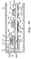
- FIGURE 1 shows a plan view and a sectional elevation of a dielectric body 21 for the feedthrough capacitor 20.
- FIGURE 2 shows a manufacturing process of the feedthrough capacitor 20.
- the dielectric body 21 made of ceramic is defined a through hole 22 at the center of the ceramic dielectric 21.
- a pair of electrodes 23 and 24 are attached on both sides of the ceramic dielectric 21 in orthogonal to the hole 22, as shown in FIGURE 2 (a).
- the electrodes 23 and 24 are defined holes with a diameter larger than the diameter of the through hole 22, respectively.
- a tin-coat conductive rod 25 is fit through the hole 21, as shown in FIGURE 2 (b).
- One end 25a of the conductive rod 25 is soldered to the electrode 23 with solder 26.
- Other end 25b of the conductive rod 25 is extended through the electrode 24 without any conduction to the electrode 24.
- the feedthrough capacitor 20 is formed.
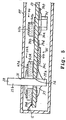
- FIGURE 3 is a sectional elevation showing a conventional thick-film high frequency signal circuit apparatus 29.
- the electrode 24 of the feedthrough capacitor 20 is soldered or bonded to the shielding case 27 by conductive bond 30, so that the conductive rod 25 penetrates both opposite walls of the shielding case 27 through holes 31 and 32 defined in the walls of the shielding case 27.
- the conventional thick-film high frequency signal circuit apparatus 29, as shown in FIGURE 3 comprises the feedthrough capacitor 20, the shielding case 27 and the thick-film circuit 28 housed inside the shielding case 27.
- the thick-film circuit 28 is constituted on a substrate 33.
- Some conductive layers 34a, 34b, 34c,... and some thick-film electrical components, e.g., a thick-film resistor 35 are formed on the substrate 33 by a conventional thick-film technique.
- the substrate 33 defines a through hole 36 at a position facing the feedthrough capacitor 20.
- the conductive rod 25 passes therethrough.
- the middle part of the conductive rod 25 is soldered to one of the conductive layers, i.e., the conductive layer 34a around the hole 36 on the substrate 33 by solder 37.
- the conductive rod 25 of the feedthrough capacitor 20 is coupled to a signal line in the thick-film circuit 28 through the conductive layer 34a. Furthermore, the head of the other end 25b of the conductive rod 25 protrudes from the opposite wall of the shielding case 27. The protruding end of the conductive rod 25 constitutes a pin terminal 38 for receiving input signals to the thick-film high frequency signal circuit apparatus 29 or outputting signals therefrom.
- the conventional thick-film high frequency signal circuit apparatus as shown in FIGURE 3 , has some drawbacks as follows.
- the feedthrough capacitor 20 is mounted outside the shielding case 27.
- the thick-film high frequency signal circuit apparatus 29 becomes large in size.
- Feedthrough capacitor 20 gives a poor appearance as it projects out of the shielding case 27.
- the feedthrough capacitor 20 also has an insufficient moisture-resistance due to the feedthrough capacitor 20 being mounted outside the shielding case 27.
- a manufacturing process of the thick-film high frequency signal circuit apparatus 29 is very complicated. That is, the feedthrough capacitor 20 must be soldered to both the shielding case 27 and the conductive layer 24c of the thick-film circuit 28 after the thick-film circuit 28 is housed in the shielding case 27.
- FIGURE 4 is an equivalent circuit diagram of the thick-film high frequency signal circuit apparatus 29, in which a plurality of the feedthrough capacitor 20 are provided for receiving signals therein or outputting signals therefrom.
- the feedthrough capacitor 20 is coupled to the opposite side of the pin terminal 38 in respect to the signal line, i.e., the conductive layer 34c.
- the signal line i.e., the conductive layer 34c.
- Another object of the present invention to provide a thick-film high frequency signal circuit apparatus in which the feedthrough capacitor has a good moisture-resistance.
- a further object of the present invention to provide a thick-film high frequency signal circuit apparatus which is easy to manufacture.
- a still further object of the present invention to provide a thick-film high frequency signal circuit apparatus which has a sufficient noise reducing characteristics.
- a thick-film high frequency signal circuit apparatus which includes a thick-film circuit in which a high frequency signal circuit is constituted on a substrate in a thick-film configuration, a shielding case for housing the thick-film circuit therein, a feedthrough capacitor constituted on one surface of the substrate in the thick-film configuration and a terminal for transmitting signals between the thick-film circuit and a circuit outside the shielding case, the terminal having a first end coupled to the thick-film circuit through the feedthrough capacitor and a second end protruding outside the shielding case through a hole defined therein.
- FIGURES 5 through 18 The present invention will be described in detail with reference to the FIGURES 5 through 18 .
- reference numerals or letters used in FIGURES 1 , 2 , 3 and 4 will be used to designate like or equivalent elements for simplicity of explanation.
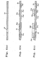
- FIGURES 5 , 6 , 7 and 8 a first embodiment of the thick-film high frequency signal circuit apparatus with an improved feedthrough capacitor according to the present invention will be described in detail.
- FIGURE 5 is a sectional elevation of the embodiment of the thick-film high frequency signal circuit apparatus 29a with a feedthrough capacitor.
- the thick-film high frequency signal circuit apparatus 29a comprises a thick-film circuit 28a and a shielding case 27 for housing the thick-film circuit 28a.
- the thick-film circuit 28a is constituted on a substrate 33 made of such as the alumina, etc.
- the thick-film circuit 28a comprises a feedthrough capacitor section 20a, a thick-film resistor 35, a regular thick-film capacitor section 40 and a chip transistor 41.
- the substrate 33 is made of ceramic, e.g., alumina.
- the substrate 33 defines a hole 36.
- the hole 36 is cut through by a laser beam.
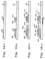
- Some conductive layers 34a, 34b, 34c, 34d, 34e, 34f are coated on the substrate 33 according to a conventional screen printing, as shown in FIGURE 6 (b).
- the conductive layers 34a and 34c are shaped in a rectangular ring shape around the hole 36 at both surfaces of the substrate 33.
- the other conductive layers 34b, 34d, 34e and 34f are shaped to a rectangular shape.
- the conductive layers 34a, 34b, 34c, 34d, 34e, 34f are made of a silver or a palladium base conductive paste.
- dielectric layers 42a and 42b are coated on the conductive layers 34a and 34b according to the screen printing, as shown in FIGURE 6 (c).
- the dielectric layers 42a on the conductive layer 34a is formed in a rectangular ring shape in correspondence with the shape of the conductive layer 34a.
- the dielectric layer 42b on the conductive layer 34b is formed in a rectangular shape in correspondence with the shape of the conductive layer 34b.
- the dielectric layers 42a and 42b are made of ceramic paste having a high permittivity.
- conductive layers 43a and 43b are coated on the dielectric layers 42a and 42b according to the screen printing, as shown in FIGURE 6 (d).
- the conductive layers 43a and 43b are shaped in the rectangular ring shape around the hole 36 and the rectangular shape, in similar to the conductive layers 34a and 34b, respectively.
- a part of the conductive layers 43b elongates onto the substrate 33 along the dielectric layer 42b.
- the conductive layers 43a and 43b are also made of the silver or the palladium base conductive paste.
- the structure of FIGURE 6 (d) is heated at 900°C for one hour so that the feedthrough capacitor section 20a and the regular thick-film capacitor 40 are formed on the substrate 33.
- the conductive layer 34a constitutes a bottom electrode which will be electrically coupled to the shielding case 27.
- the conductive layer 34a will be referred as the bottom electrode 34a of the feedthrough capacitor section 20a.
- the conductive layer 43a constitutes a top electrode which will be electrically coupled to a pin terminal 38 for receiving input signals to the thick-film high frequency signal circuit apparatus 29a or outputting signals therefrom for the shielding case 27.
- the conductive layer 43a will be referred as the top electrode 43a of the feedthrough capacitor section 20a.
- the conductive layers 34b and 43b constitute bottom and top electrodes of the thick-film capacitor section 40.
- the conductive layers 34b and 43b will be referred as the bottom and top electrodes 34b and 43b of the thick-film capacitor section 40, in similar to the feedthrough capacitor section 20a.
- a resistive layer 44 is coated on the substrate 33, as shown in FIGURE 6 (e). Both ends of the resistive layer 44 are overlapped on ends of the conductive layers 34c and 34d.
- the resistive layer 44 is made of ruthenium oxide base resistive paste. Then, the structure of FIGURE 6 (e) is heated at 850°C for one hour so that the thick-film resistor 35 is formed on the substrate 33.
- the conductive layers 34e and 34f are used for electrical contact with the chip transistor 41, as shown in FIGURE 5 .
- the thick-film circuit 28a includes three feedthrough capacitor sections 20a.
- Each of the feedthrough capacitor sections 20a is formed to the rectangular ring shape, as described above. However, the feedthrough capacitor sections 20a can be formed in the round ring shape.
- Each of the feedthrough capacitor sections 20a comprises the bottom electrode 34a, the dielectric layer 42a and the top electrode 43a.
- a part of the bottom electrode 34a is elongated from the rectangular ring portion so that the elongated portion 34a-e can be used for electrical coupling to some other circuit.
- Each of the feedthrough capacitor sections 20a is formed to a size in that the dielectric layer made of the above-mentioned ceramic paste has an area of 3.52 mm2. As a result, these feedthrough capacitor sections 20a have had a capacitance as large as 4000 pF to 4500 pF.
- the capacitance of the feedthrough capacitor section 20a is realized by such a small area less than half of that of the conventional feedthrough capacitor 20 of FIGURES 2 and 3 .
- the thick-film high frequency signal circuit apparatus 29a is provided with a tin-coat conductive rod 25, as shown in FIGURE 5 .
- the conductive rod 25 fits through the hole 42 of the substrate 33 before housing the structure of FIGURE 6 (e) into the shielding case 29.
- One end 25a of the conductive rod 25 is soldered to both the conductive layers 34a and 34c by solder 37.
- Another end 25b of the the conductive rod 25 protrudes the outside of the shielding case 27 through a hole 31 defined in the wall of the shielding case 27.
- the end 25a of the conductive rod 25 constitutes a pin terminal 38 for receiving input signals into the thick-film high frequency signal circuit apparatus 29a or outputting signals therefrom.
- the elongated portion 34a-e of the bottom electrode 34a is coupled to the shielding case 27 through a conductive wire 45.
- the thick-film high frequency signal circuit apparatus 29a includes three feedthrough capacitor sections 20a, in similar to the the thick-film circuit 28a of FIGURE 7 . These three feedthrough capacitor sections 20a are provided for receiving signals into the thick-film high frequency signal circuit apparatus 29a or outputting signals therefrom through the pin terminals 38.
- the feedthrough capacitor sections 20a are positioned between the pin terminals 38 and signal lines 46 which are constituted by the conductive layers 34c or coupled to thereto (see FIGURE 5 ).
- the feedthrough capacitor sections 20a are desirable in comparison to the conventional feedthrough capacitor 20, as shown in FIGURE 4 , when viewed from the noise reducing object against noises, such as the electromagnetic disturbance incoming or outgoing through the pin terminals 38.
- the thick-film high frequency signal circuit apparatus 29a has the feedthrough capacitor sections 20a in the shielding case 27.
- the thick-film high frequency signal circuit apparatus 29a becomes compact in size and gives a good appearance since the feedthrough capacitor sections 20a is contained in the shielding case 27.
- the feedthrough capacitor sections 20a are formed simultaneously in the manufacturing process of the regular thick-film capacitor 40.
- the thick-film high frequency signal circuit apparatus 29a can be easily realized without spending any extra costs and processes for the feedthrough capacitor sections 20a.
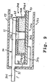
- FIGURES 9 , 10 and 11 a second embodiment of the thick-film high frequency signal circuit apparatus with an improved feedthrough capacitor according to the present invention will be described in detail.
- reference numerals or letters used in FIGURES 5 , 6 , 7 and 8 (first embodiment) will be used to designate like or equivalent elements for simplicity of explanation.
- FIGURE 9 is a sectional elevation of the embodiment of the thick-film high frequency signal circuit apparatus 29a with a feedthrough capacitor.
- the thick-film high frequency signal circuit apparatus 29a comprises a thick-film circuit 28a and a shielding case 27 for housing the thick-film circuit 28a.
- a part corresponding to a feedthrough capacitor section 20a is shown in respect to the thick-film circuit 28a.
- the thick-film circuit 28a can be provided with other thick-film components such as the feedthrough capacitor section 20a, the thick-film resistor 35, the regular thick-film capacitor section 40 and the chip transistor 41 in the first embodiment.
- the thick-film circuit 28a is constituted on a substrate 33 made of such as the alumina, etc., in similar to the first embodiment.
- a conductive layer 34a is coated on the substrate 33 according to the conventional screen printing.
- the conductive layer 34a is shaped in a rectangular shape.
- the conductive layer 34a is made of the silver or the palladium base conductive paste, in similar to the first embodiment.
- a dielectric layer 42a is coated on the conductive layer 34a according to the screen printing.
- the dielectric layer 42a is formed in the rectangular ring shape so that the dielectric layer 42a defines a rectangular hole 47 in correspondence with the conductive layer 34a.
- the hole 37 exposes the conductive layer 34a.
- the dielectric layer 42a is made of ceramic paste, in similar to the first embodiment.
- a conductive layer 43a is coated on the dielectric layer 42a according to the screen printing.
- the conductive layer 43a is also made of the silver or the palladium base conductive paste.
- the conductive layer 43a is also shaped in the rectangular ring shape in correspondence with the dielectric layer 42a. A part of the conductive layer 43a elongates to the substrate 33 along the dielectric layer 42a. The elongated potion 43a-e of the conductive layer 43a can be used for electrical coupling to some other circuit.
- the above-mentioned structure constituted on the substrate 33 is heated at 900°C for one hour so that the feedthrough capacitor section 20a is formed on the substrate 33 simultaneously with the manufacturing process of some other regular thick-film capacitor section such as the regular thick-film capacitor section 40 of the first embodiment.
- the conductive layer 34a constitutes a bottom electrode which will be electrically coupled to the shielding case 27.
- the conductive layer 34a will be referred as the bottom electrode 34a of the feedthrough capacitor section 20a, in similar to the first embodiment.
- the conductive layer 43a constitutes a top electrode which will be electrically coupled to a pin terminal 38 for receiving input signals to the thick-film high frequency signal circuit apparatus 29a or outputting signals therefrom for the shielding case 27.
- the conductive layer 43a will be also referred as the top electrode 43a of the feedthrough capacitor section 20a.
- an insulative cover 48 is coated on the feedthrough capacitor section 20a.
- the insulative cover 48 is formed in the rectangular cylinder shape so that the insulative cover 48 covers the feedthrough capacitor section 20a.
- the insulative cover 48 defines a borehole 49 in correspondence with the hole 47 of the dielectric layer 42a.
- the feedthrough capacitor sections 20a is formed to the rectangular ring shape, as described above. However, the feedthrough capacitor sections 20a can be formed in the round ring shape.
- the feedthrough capacitor sections 20a comprises the bottom electrode 34a, the dielectric layer 42a, the top electrode 43a and the insulative cover 48.
- the bottom electrode 34a and the top electrode 43a are provided with the elongated portions 34a-e and 43a-e for use of electrical couplings to some other circuits.
- the thick-film high frequency signal circuit apparatus 29a is provided with a tin-coat conductor 50, as shown in FIGURE 9 .
- the conductor 50 is mounted to the thick-film circuit 28a before housing the thick-film circuit 28a in the shielding case 27.
- One end of the conductor 50 forks into two branches 50a and 50b.
- the branches 50a and 50b fit to the feedthrough capacitor sections 20a so that the conductor 50 is mounted to the thick-film circuit 28a.
- One branch 50a of the conductor 50 is coupled to the bottom electrode 34a through conductive paste 51 filled in the hole 47 of the dielectric layer 42a and the borehole 49 of the insulative cover 48.
- the other branch 50b of the conductor 50 is attached to a rear surface of the substrate 33.
- Another end 50c of the conductor 50 protrudes the outside of the shielding case 27 through a hole 31 defined in the sidewall of the shielding case 27.
- the end 50c of the conductor 50 constitutes a pin terminal 38 for receiving input signals into the thick-film high frequency signal circuit apparatus 29a or outputting signals therefrom.
- the elongated portion 34a-e of the bottom electrode 34a is coupled to the shielding case 27 through a conductive wire 45.
- FIGURE 11 an equivalent circuit diagram of the thick-film high frequency signal circuit apparatus 29a will be described.
- a plurality of the feedthrough capacitor sections 20a are provided for receiving signals into the thick-film high frequency signal circuit apparatus 29a or outputting signals therefrom.
- each of the feedthrough capacitor sections 20a are positioned between the pin terminals 38 and signal lines 46 which are constituted by the conductive layers 34c or coupled thereto (see FIGURE 9 ).
- the feedthrough capacitor sections 20a are desirable in comparison to the conventional feedthrough capacitor 20, as shown in FIGURE 4 , when viewed from the noise reducing object against noises, such as the electromagnetic disturbance incoming or outgoing through the pin terminals 38.
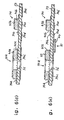
- FIGURES 12 and 13 a third embodiment of the thick-film high frequency signal circuit apparatus with an improved feedthrough capacitor according to the present invention will be described in detail.
- FIGURE 12 is a sectional elevation of the embodiment of the thick-film high frequency signal circuit apparatus 29a with a feedthrough capacitor section.
- the thick-film high frequency signal circuit apparatus 29a comprises a thick-film circuit 28a and a shielding case 27 for housing the thick-film circuit 28a.
- the thick-film circuit 28a is constituted on a substrate 33 made of such as the alumina, etc.
- the thick-film circuit 28a comprises a feedthrough capacitor section 20a, a thick-film resistor 35, a regular thick-film capacitor section 40, a chip transistor 41 and a jumper wiring section 52.
- the substrate 33 is made of ceramic, e.g., alumina.
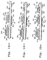
- Two conductive layers 34a and 34b are coated on the substrate 33 according to a conventional screen printing, as shown in FIGURE 13 (a).
- the conductive layers 34a and 34b are made of the silver or the palladium base conductive paste, in similar to the first embodiment.
- Dielectric layers 42a and 42b are coated on the conductive layers 34a and 34b according to the screen printing, as shown in FIGURE 13 (b).
- the dielectric layers 42a and 42b almost cover the conductive layers 34a and 34b, respectively. But, a part of each of the conductive layers 34a and 34b elongates outside the dielectric layers 42a and 42b along the substrate 33.
- the dielectric layers 42a and 42b are made of ceramic paste having a high permittivity.
- Conductive layers 43a and 43b are coated on the dielectric layers 42a and 42b according to the screen printing, as shown in FIGURE 13 (c). A part of the conductive layer 43b elongates onto the substrate 33 along the side of the dielectric layer 42b.
- the conductive layers 43a and 43b are also made of the silver or the palladium base conductive paste.
- the structure of FIGURE 13 (c) is heated at 900°C for one hour so that the feedthrough capacitor section 20a and the regular thick-film capacitor 40 are formed on the substrate 33.
- the conductive layer 34a constitutes a bottom electrode which will be electrically coupled to the shielding case 27.
- the conductive layer 34a will be referred as the bottom electrode 34a of the feedthrough capacitor section 20a.
- the conductive layer 43a constitutes a top electrode which will be electrically coupled to a pin terminal 38 for receiving input signals to the thick-film high frequency signal circuit apparatus 29a or outputting signals therefrom for the shielding case 27.
- the conductive layer 43a will be referred as the top electrode 43a of the feedthrough capacitor section 20a.
- the conductive layers 34b and 43b constitute bottom and top electrodes of the thick-film capacitor section 40.
- the conductive layers 34b and 43b will be referred as the bottom and top electrodes 34b and 43b of the thick-film capacitor section 40, in similar to the feedthrough capacitor section 20a.
- Insulative covers 48a and 48b are coated to cover the feedthrough capacitor section 20a and the regular thick-film capacitor 40, as shown in FIGURE 13 (d).
- the insulative cover 48a defines a borehole 49 so that the top electrode 43a exposes through the borehole 49.
- FIGURE 13 (d) a resistive layer 44 is coated on the substrate 33, as shown in FIGURE 13 (d).
- the resistive layer 44 is made of ruthenium oxide base resistive paste. Then, the structure of FIGURE 13 (d) is heated at 850°C for one hour so that the thick-film resistor 35 is formed on the substrate 33.
- a conductive layer 53 is coated on the insulative cover 48a of the feedthrough capacitor section 20a, as shown in FIGURE 13 (e). A part of the conductive layer 53 fills in the borehole 49 of the insulative cover 48a so that the conductive layer 53 is coupled to the top electrode 43a of the feedthrough capacitor section 20a. Simultaneously to the forming of the conductive layer 53, some other conductive layers 34c to 34h are coated on the substrate 33. A part of each of the conductive layers 34d and 34e are overlapped to ends of the thick-film resistor 35. The conductive layers 34f and 34g will be used for for electrical contact with the chip transistor 41, as shown in FIGURE 12 .
- An insulative covers 48c is coated to cover the conductive layer 34h, as shown in FIGURE 13 (f).
- a conductive layer 54 is coated on the insulative covers 48c, as shown in FIGURE 13 (g).
- the conductive layer 54 is isolated from the conductive layer 34h by the insulative cover 48c.
- the jumper wiring section 52 is formed on the substrate 33.
- the thick-film high frequency signal circuit apparatus 29a is provided with a tin-coat conductor 50, as shown in FIGURE 12 .
- the conductor 50 is mounted to the thick-film circuit 28a before housing the thick-film circuit 28a in the shielding case 27.
- One end of the conductor 50 forks into two branches 50a and 50b.
- the branches 50a and 50b fit to the feedthrough capacitor sections 20a so that the conductor 50 is mounted to the thick-film circuit 28a.
- One branch 50a of the conductor 50 is soldered to the conductive layer 53 so that the conductor 50 is coupled to the top electrode 43a through the conductive layer 53.
- the other branch 50b of the conductor 50 is soldered to the conductive layer 34c.
- Another end 50c of the conductor 50 protrudes the outside of the shielding case 27 through a hole 31 defined in the sidewall of the shielding case 27.
- the end 50c of the conductor 50 constitutes a pin terminal 38 for receiving input signals into the thick-film high frequency signal circuit apparatus 29a or outputting signals therefrom.
- the elongated portions 34a-e of the bottom electrode 34a is electrically coupled to the shielding case 27 through a conductive wire 45.
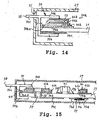
- FIGURE 14 is a sectional elevation of the modification of the third embodiment of the thick-film high frequency signal circuit apparatus 29a with a feedthrough capacitor.
- the thick-film high frequency signal circuit apparatus 29a comprises a thick-film circuit 28a and a shielding case 27 for housing the thick-film circuit 28a.
- a part corresponding to a feedthrough capacitor section 20a is shown in respect to the thick-film circuit 28a.
- the thick-film circuit 28a can be provided with other thick-film components such as the feedthrough capacitor section 20a, the thick-film resistor 35, the regular thick-film capacitor section 40 and the chip transistor 41 in the first embodiment.
- the thick-film circuit 28a is constituted on a substrate 33 made of such as the alumina, etc., in similar to the first embodiment.
- a conductive layer 34a is coated on the substrate 33 according to the conventional screen printing.
- the conductive layer 34a is made of the silver or the palladium base conductive paste, in similar to the first embodiment.
- a dielectric layer 42a is coated on the conductive layer 34a according to the screen printing.
- the dielectric layer 42a almost covers the conductive layer 34a. But, a part of the conductive layer 34a elongates outside the dielectric layer 42a along the substrate 33.
- the dielectric layer 42a is made of ceramic paste, in similar to the first embodiment.
- a conductive layer 43a is coated on the dielectric layer 42a according to the screen printing.
- the conductive layer 43a is also made of the silver or the palladium base conductive paste.
- a part of the conductive layer 43a elongates to the substrate 33 along the side of the dielectric layer 42a.
- the elongated portion 43a-e of the conductive layer 43a can be used for electrical coupling to some other circuit.
- the above-mentioned structure constituted on the substrate 33 is heated at 900°C for one hour so that the feedthrough capacitor section 20a is formed on the substrate 33 simultaneously with the manufacturing process or some other regular thick-film capacitor section such as the regular thick-film capacitor section 40 of the third embodiment.
- the conductive layer 34a constitutes a bottom electrode which will be electrically coupled to the shielding case 27.
- the conductive layer 34a will be referred as the bottom electrode 34a of the feedthrough capacitor section 20a, in similar to the first embodiment.
- the conductive layer 43a constitutes a top electrode which will be electrically coupled to a pin terminal 38 for receiving input signals to the thick-film high frequency signal circuit apparatus 29a or outputting signals therefrom for the shielding case 27.
- the conductive layer 43a will be also referred as the top electrode 43a of the feedthrough capacitor section 20a.
- an insulative cover 48a is coated to almost cover the feedthrough capacitor section 20a.
- a part of the bottom electrode 34a elongates outside to insulative cover 48a.
- the elongated portion 34a-e of the bottom electrode 34a can be used for electrical coupling to some other circuit.
- the elongated portion 43a-e of the top electrode 43a also elongates outside the insulative cover 48a.
- a conductive layer 53 is coated on the insulative cover 48a. A part of the conductive layer 53 elongates onto the elongated portion 43a-e of the top electrode 43a along the side of the insulative cover 48a. Thus, the conductive layer 53 is coupled to the top electrode 43a.
- a conductive layer 34c is coated on the surface of the substrate 33 in correspondence with the feedthrough capacitor section 20a.
- the thick-film high frequency signal circuit apparatus 29a is provided with a tin-coat conductor 50, as shown in FIGURE 14 .
- the conductor 50 is mounted to the thick-film circuit 28a before housing the thick-film circuit 28a in the shielding case 27.
- One end of the conductor 50 forks into two branches 50a and 50b.
- the branches 50a and 50b fit to the feedthrough capacitor sections 20a so that the conductor 50 is mounted to the thick-film circuit 28a.
- One branch 50a of the conductor 50 is soldered to the conductive layer 53 so that the conductor 50 is coupled to the top electrode 43a through the conductive layer 53.
- the other branch 50b of the conductor 50 is soldered to the conductive layer 34c.
- Another end 50c of the conductor 50 protrudes the outside of the shielding case 27 through a hole 31 defined in the sidewall of the shielding case 27.
- the end 50c of the conductor 50 constitutes a pin terminal 38 for receiving input signals into the thick-film high frequency signal circuit apparatus 29a or outputting signals therefrom.
- the elongated portion 34a-e of the bottom electrode 34a is electrically coupled to the shielding case 27 through a conductive wire 45.
- FIGURE 15 a fourth embodiment of the thick-film high frequency signal circuit apparatus according to the present invention will be described in detail.
- reference numerals or letters used in FIGURES 5 , 9 and 12 first, second and third embodiments will be used to designate like or equivalent elements for simplicity of explanation.
- FIGURE 15 is a sectional elevation of the fourth embodiment of the thick-film high frequency signal circuit apparatus 29a with a feedthrough capacitor section.
- the thick-film high frequency signal circuit apparatus 29a comprises a thick-film circuit 28a and a shielding case 27 for housing the thick-film circuit 28a.
- the thick-film circuit 28a is constituted on a substrate 33 made of such as the alumina, etc.
- the thick-film circuit 28a comprises a feedthrough capacitor section 20a, a thick-film resistor 35, a regular thick-film capacitor section 40 and a chip transistor 41.
- the substrate 33 is made of ceramic, e.g., alumina.
- the substrate 33 defines a hole 36.
- the hole 36 is cut through by the laser beam, in similar to the first embodiment.
- Some conductive layers 34a to 34g are coated on the substrate 33 according to the conventional screen printing. These conductive layers 34a to 34g are made of the silver or the palladium base conductive paste, in similar to the first embodiment.
- the conductive layers 34a and 34c are shaped in a rectangular ring shape around the hole 36 at both surfaces of the substrate 33.
- the other conductive layers 34b, 34d, 34e, 34f and 34g are shaped to a rectangular shape.
- a dielectric layer 42a is coated on the conductive layer 34a according to the screen printing.
- the dielectric layer 42a on the conductive layer 34a is formed in a rectangular ring shape in correspondence with the shape of the conductive layer 34a.
- the dielectric layer 42a is made of ceramic paste, in similar to the first embodiment.
- a conductive layer 43a is coated on the dielectric layer 42a according to the screen printing.
- the conductive layer 43a is also made of the silver or the palladium base conductive paste.
- the conductive layer 43a is shaped in the rectangular ring shape around the hole 36 and the rectangular shape, in similar to the conductive layers 34a and 34b, respectively.
- the conductive layer 43a elongates onto the inner wall of the dielectric layer 42b.
- the inner wall of the dielectric layer 42a is covered with the conductive layer 43a.
- the conductive layer 34c coated on the other surface of the substrate 33 elongates into the inner wall of the hole 36.
- the inner wall of the hole 36 is covered with the conductive layer 34c.
- the conductive layer 34a constitutes a bottom electrode which will be electrically coupled to the shielding case 27.
- the conductive layer 34a will be referred as the bottom electrode 34a of the feedthrough capacitor section 20a, in similar to the first embodiment.
- the conductive layer 43a constitutes a top electrode which will be electrically coupled to a pin terminal 38 for receiving input signals to the thick-film high frequency signal circuit apparatus 29a or outputting signals therefrom for the shielding case 27.
- the conductive layer 43a will be also referred as the top electrode 43a of the feedthrough capacitor section 20a.
- the thick-film high frequency signal circuit apparatus 29a is provided with a tin-coat conductor 50, as shown in FIGURE 15 .
- the conductor 50 is mounted to the thick-film circuit 28a before housing the thick-film circuit 28a in the shielding case 27.
- One end of the conductor 50 forks into two branches 50a and 50b.
- the branches 50a and 50b fit to the feedthrough capacitor sections 20a so that the conductor 50 is mounted to the thick-film circuit 28a.
- One branch 50a of the conductor 50 is soldered to the top electrode 43a so that the conductor 50 is coupled to the conductive layer 34c through the feedthrough 55.
- the other branch 50b of the conductor 50 is attached to the other surface of the substrate 33.
- Another end 50c of the conductor 50 protrudes the outside of the shielding case 27 through a hole 31 defined in the sidewall of the shielding case 27.
- the end 50c of the conductor 50 constitutes a pin terminal 38 for receiving input signals into the thick-film high frequency signal circuit apparatus 29a or outputting signals therefrom.
- the elongated portion 34a-e of the bottom electrode 34a is electrically coupled to the shielding case 27 through a conductive wire 45.
- FIGURES 16 , 17 and 18 a fifth embodiment of the thick-film high frequency signal circuit apparatus according to the present invention will be described in detail.
- reference numerals or letters used in FIGURES 5 , 9 , 12 and 15 first, second, third and fourth embodiments will be used to designate like or equivalent elements for simplicity of explanation.
- FIGURE 16 is a sectional elevation of the fifth embodiment of the thick-film high frequency signal circuit apparatus 29a with a feedthrough capacitor section.
- the thick-film high frequency signal circuit apparatus 29a comprises a thick-film circuit 28a and a shielding case 27 for housing the thick-film circuit 28a.
- the thick-film circuit 28a is constituted on a substrate 33 made of such as the alumina, etc.
- the thick-film circuit 28a comprises a feedthrough capacitor section 20a, a thick-film resistor 35, a regular thick-film capacitor section 40 and a chip transistor 41.
- the substrate 33 is made of ceramic, e.g., alumina.
- the substrate 33 defines a hole 36.
- the hole 36 is cut through by the laser beam, in similar to the first and fourth embodiments.
- Some conductive layers 34a to 34g are coated on the substrate 33 according to the conventional screen printing. These conductive layers 34a to 34g are made of the silver or the palladium base conductive paste, in similar to the first embodiment.
- the conductive layers 34a and 34c are shaped in a round ring shape around the hole 36 at both surfaces of the substrate 33.
- the other conductive layers 34b, 34d, 34e, 34f and 34g are shaped to a rectangular shape.
- a dielectric layer 42a is coated on the conductive layer 34a according to the screen printing.
- the dielectric layer 42a on the conductive layer 34a is formed in a round ring shape in correspondence with the shape of the conductive layer 34a.
- the dielectric layer 42a is made of ceramic paste, in similar to the first embodiment.
- a conductive layer 43a is coated on the dielectric layer 42a according to the screen printing.
- the conductive layer 43a is also made of the silver or the palladium base conductive paste.
- the conductive layer 43a is shaped in the round ring shape around the hole 36, in similar to the conductive layer 34a and the dielectric layer 42a.
- a part of the conductive layer 43a elongates onto the substrate 33 along the side of the dielectric layer 42a.
- the elongated portion 43a-e of the conductive layer 43a can be used for electrical coupling to some other circuit.
- the above-mentioned structure constituted on the substrate 33 is heated at 900°C for one hour so that the feedthrough capacitor section 20a is formed on the substrate 33 simultaneously with the manufacturing process of some other regular thick-film capacitor section such as the regular thick-film capacitor section 40.
- the conductive layer 34a constitutes a bottom electrode which will be electrically coupled to the shielding case 27.
- the conductive layer 34a will be referred as the bottom electrode 34a of the feedthrough capacitor section 20a, in similar to the first embodiment.
- the conductive layer 43a constitutes a top electrode which will be electrically coupled to a pin terminal 38 for receiving input signals to the thick-film high frequency signal circuit apparatus 29a or outputting signals therefrom for the shielding case 27.
- the conductive layer 43a will be also referred as the top electrode 43a of the feedthrough capacitor section 20a.
- An insulative cover 48a is coated on the feedthrough capacitor section 20a.
- the insulative cover 48a is formed in the round cylinder shape with a center hole 56 so that the insulative cover 48a covers the feedthrough capacitor section 20a.
- a conductive layer 53 is coated on the insulative cover 48a.
- the conductive layer 53 elongates onto the inner wall of the dielectric layer 42b.
- the inner wall of the center hole 56 of the dielectric layer 42a is covered with the conductive layer 53.
- the conductive layer 34c coated on the other surface of the substrate 33 elongates into the inner wall of the hole 36.
- the inner wall of the hole 36 is covered with the conductive layer 34c.
- the conductive layer 53 further elongates onto the substrate 33 along the side of the insulative cover 48a. A halfway of the elongated portion 53e of the conductive layer 53 is coupled to the elongated portion 34a-e of the conductive layer 34a. Thus, the conductive layer 34a is coupled to the conductive layer 34c on the other surface of the substrate 33 through the conductive layer 53 and the feedthrough 55.
- the thick-film high frequency signal circuit apparatus 29a is provided with a tin-coat conductor 50, as shown in FIGURE 16 .
- the conductor 50 is mounted to the thick-film circuit 28a before housing the thick-film circuit 28a in the shielding case 27.
- One end of the conductor 50 forks into two branches 50a and 50b.
- the branches 50a and 50b fit to the feedthrough capacitor sections 20a so that the conductor 50 is mounted to the thick-film circuit 28a.
- One branch 50a of the conductor 50 is soldered to the elongated portion 53e of the conductive layer 53.
- the other branch 50b of the conductor 50 is attached to the other surface of the substrate 33.
- Another end 50c of the conductor 50 protrudes the outside of the shielding case 27 through a hole 31 defined in the sidewall of the shielding case 27.
- the end 50c of the conductor 50 constitutes a pin terminal 38 for receiving input signals into the thick-film high frequency signal circuit apparatus 29a or outputting signals therefrom.
- the elongated portion 34a-e of the bottom electrode 34a is coupled to the shielding case 27 through a conductive wire 45.
- the feedthrough capacitor sections 20a is formed to the round ring shape, as described above. However, the feedthrough capacitor sections 20a can be formed in the rectangular ring shape.
- the feedthrough capacitor sections 20a comprises the bottom electrode 34a, the dielectric layer 42a, the top electrode 43a and the insulative cover 48a.
- the bottom electrode 34a, the top electrode 43a and the conductive layer 53 are provided with the elongated portions 34a-e, 43a-e and 53e.
- the elongated portion 34a-e of the bottom electrode 34a is electirically coupled to the shielding case 27 through a conductive layer 45a coated on the substrate 33.
- the elongated portions 43a-e and 53e of the top electrode and the conductive layer 53 are coupled together, as described above. Then, the end 50a of the conductor 50 is soldered to the elongated portion 53e of the conductive layer 53, as described above.
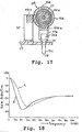
- FIGURE 18 is a graph showing the high frequency noise reducing characteristics for both the conventional apparatus, as shown in FIGURE 3 , and the fifth embodiment of the apparatus according to the present invention, as shown in FIGURE 16 .
- Graph A is the characteristics of the conventional apparatus.
- Graph B is the characteristics of the fifth embodiment of the apparatus according to the present invention.
- Graph B has the improved noise reduction characteristics in the lower frequency region in compared to the characteristics of Graph A.
- Graph B also has the noise reduction characteristics comparative to the characteristics of Graph A in the higher frequency region.
- the present invention can provide an extremely preferable thick-film high frequency signal circuit apparatus with an improved feedthrough capacitor.
Landscapes
- Engineering & Computer Science (AREA)
- Microelectronics & Electronic Packaging (AREA)
- Physics & Mathematics (AREA)
- Condensed Matter Physics & Semiconductors (AREA)
- General Physics & Mathematics (AREA)
- Computer Hardware Design (AREA)
- Power Engineering (AREA)
- Fixed Capacitors And Capacitor Manufacturing Machines (AREA)
- Shielding Devices Or Components To Electric Or Magnetic Fields (AREA)
- Parts Printed On Printed Circuit Boards (AREA)
Applications Claiming Priority (4)
| Application Number | Priority Date | Filing Date | Title |
|---|---|---|---|
| JP62275202A JPH01117014A (ja) | 1987-10-29 | 1987-10-29 | 貫通コンデンサ |
| JP275202/87 | 1987-10-29 | ||
| JP11607/88 | 1988-01-20 | ||
| JP63011607A JP2585337B2 (ja) | 1988-01-20 | 1988-01-20 | 高周波回路基板装置 |
Publications (2)
| Publication Number | Publication Date |
|---|---|
| EP0315320A2 true EP0315320A2 (fr) | 1989-05-10 |
| EP0315320A3 EP0315320A3 (fr) | 1990-02-07 |
Family
ID=26347061
Family Applications (1)
| Application Number | Title | Priority Date | Filing Date |
|---|---|---|---|
| EP88309154A Ceased EP0315320A3 (fr) | 1987-10-29 | 1988-10-03 | Circuit de signal à haute fréquence a film épais comprenant un condensateur du type "feedthrough" |
Country Status (3)
| Country | Link |
|---|---|
| US (1) | US4858064A (fr) |
| EP (1) | EP0315320A3 (fr) |
| KR (1) | KR910004957B1 (fr) |
Cited By (1)
| Publication number | Priority date | Publication date | Assignee | Title |
|---|---|---|---|---|
| EP1246326A1 (fr) * | 2001-03-30 | 2002-10-02 | Agilent Technologies, Inc. (a Delaware corporation) | Boítier électronique |
Families Citing this family (22)
| Publication number | Priority date | Publication date | Assignee | Title |
|---|---|---|---|---|
| KR0173691B1 (ko) * | 1993-07-07 | 1999-02-01 | 카나이 쯔또무 | 관통콘덴서 및 필터를 구비한 마그네트론 |
| TW443717U (en) | 1996-06-28 | 2001-06-23 | Sharp Kk | Tuner structure and cable modem tuner using the same |
| US8195295B2 (en) | 2008-03-20 | 2012-06-05 | Greatbatch Ltd. | Shielded three-terminal flat-through EMI/energy dissipating filter |
| US8761895B2 (en) * | 2008-03-20 | 2014-06-24 | Greatbatch Ltd. | RF activated AIMD telemetry transceiver |
| US11147977B2 (en) | 2008-03-20 | 2021-10-19 | Greatbatch Ltd. | MLCC filter on an aimd circuit board conductively connected to a ground pin attached to a hermetic feedthrough ferrule |
| US10080889B2 (en) | 2009-03-19 | 2018-09-25 | Greatbatch Ltd. | Low inductance and low resistance hermetically sealed filtered feedthrough for an AIMD |
| US9463329B2 (en) | 2008-03-20 | 2016-10-11 | Greatbatch Ltd. | Shielded three-terminal flat-through EMI/energy dissipating filter with co-fired hermetically sealed feedthrough |
| US8095224B2 (en) * | 2009-03-19 | 2012-01-10 | Greatbatch Ltd. | EMI shielded conduit assembly for an active implantable medical device |
| US8624478B2 (en) * | 2009-10-09 | 2014-01-07 | Mapper Lithography Ip B.V. | High voltage shielding arrangement of a charged particle lithography system |
| US9427596B2 (en) | 2013-01-16 | 2016-08-30 | Greatbatch Ltd. | Low impedance oxide resistant grounded capacitor for an AIMD |
| US10350421B2 (en) | 2013-06-30 | 2019-07-16 | Greatbatch Ltd. | Metallurgically bonded gold pocket pad for grounding an EMI filter to a hermetic terminal for an active implantable medical device |
| US10272252B2 (en) | 2016-11-08 | 2019-04-30 | Greatbatch Ltd. | Hermetic terminal for an AIMD having a composite brazed conductive lead |
| US11198014B2 (en) | 2011-03-01 | 2021-12-14 | Greatbatch Ltd. | Hermetically sealed filtered feedthrough assembly having a capacitor with an oxide resistant electrical connection to an active implantable medical device housing |
| US10596369B2 (en) | 2011-03-01 | 2020-03-24 | Greatbatch Ltd. | Low equivalent series resistance RF filter for an active implantable medical device |
| US9931514B2 (en) | 2013-06-30 | 2018-04-03 | Greatbatch Ltd. | Low impedance oxide resistant grounded capacitor for an AIMD |
| US20130046354A1 (en) | 2011-08-19 | 2013-02-21 | Greatbatch Ltd. | Implantable cardioverter defibrillator designed for use in a magnetic resonance imaging environment |
| US9504843B2 (en) | 2011-08-19 | 2016-11-29 | Greatbach Ltd. | Implantable cardioverter defibrillator designed for use in a magnetic resonance imaging environment |
| WO2014041649A1 (fr) * | 2012-09-13 | 2014-03-20 | 電気化学工業株式会社 | Composition de caoutchouc, et vulcanisat et article moulé correspondant |
| USRE46699E1 (en) | 2013-01-16 | 2018-02-06 | Greatbatch Ltd. | Low impedance oxide resistant grounded capacitor for an AIMD |
| US10249415B2 (en) | 2017-01-06 | 2019-04-02 | Greatbatch Ltd. | Process for manufacturing a leadless feedthrough for an active implantable medical device |
| US10905888B2 (en) | 2018-03-22 | 2021-02-02 | Greatbatch Ltd. | Electrical connection for an AIMD EMI filter utilizing an anisotropic conductive layer |
| US10912945B2 (en) | 2018-03-22 | 2021-02-09 | Greatbatch Ltd. | Hermetic terminal for an active implantable medical device having a feedthrough capacitor partially overhanging a ferrule for high effective capacitance area |
Citations (3)
| Publication number | Priority date | Publication date | Assignee | Title |
|---|---|---|---|---|
| US4325103A (en) * | 1978-12-28 | 1982-04-13 | Murata Manufacturing Co., Ltd. | Provisional fixing structure of electronic tuner |
| US4611882A (en) * | 1982-09-08 | 1986-09-16 | Alps Electric Co., Ltd. | High-frequency circuit device with an annular capacitor on the back of an insulated substrate |
| US4747019A (en) * | 1984-12-14 | 1988-05-24 | Murata Manufacturing Co., Ltd. | Feedthrough capacitor arrangement |
Family Cites Families (4)
| Publication number | Priority date | Publication date | Assignee | Title |
|---|---|---|---|---|
| JPS5954659U (ja) * | 1982-10-01 | 1984-04-10 | 松下冷機株式会社 | 扉体 |
| US4616655A (en) * | 1984-01-20 | 1986-10-14 | Cordis Corporation | Implantable pulse generator having a single printed circuit board and a chip carrier |
| JPH0424649Y2 (fr) * | 1985-02-18 | 1992-06-11 | ||
| JPS62180882U (fr) * | 1986-05-08 | 1987-11-17 |
-
1988
- 1988-09-30 KR KR1019880012885A patent/KR910004957B1/ko not_active IP Right Cessation
- 1988-10-03 EP EP88309154A patent/EP0315320A3/fr not_active Ceased
- 1988-10-03 US US07/251,747 patent/US4858064A/en not_active Expired - Fee Related
Patent Citations (3)
| Publication number | Priority date | Publication date | Assignee | Title |
|---|---|---|---|---|
| US4325103A (en) * | 1978-12-28 | 1982-04-13 | Murata Manufacturing Co., Ltd. | Provisional fixing structure of electronic tuner |
| US4611882A (en) * | 1982-09-08 | 1986-09-16 | Alps Electric Co., Ltd. | High-frequency circuit device with an annular capacitor on the back of an insulated substrate |
| US4747019A (en) * | 1984-12-14 | 1988-05-24 | Murata Manufacturing Co., Ltd. | Feedthrough capacitor arrangement |
Non-Patent Citations (1)
| Title |
|---|
| R.C.A. TECHNICAL NOTES, no. 1317, 27th October 1982, sheets 1-3, A Publication of RCA, Princeton, New Jersey, US; J.P. HEENAN et al.: "Method for attaching edge terminals" * |
Cited By (1)
| Publication number | Priority date | Publication date | Assignee | Title |
|---|---|---|---|---|
| EP1246326A1 (fr) * | 2001-03-30 | 2002-10-02 | Agilent Technologies, Inc. (a Delaware corporation) | Boítier électronique |
Also Published As
| Publication number | Publication date |
|---|---|
| US4858064A (en) | 1989-08-15 |
| EP0315320A3 (fr) | 1990-02-07 |
| KR910004957B1 (ko) | 1991-07-18 |
| KR890007628A (ko) | 1989-06-20 |
Similar Documents
| Publication | Publication Date | Title |
|---|---|---|
| US4858064A (en) | Thick-film high frequency signal circuit apparatus with feedthrough capacitor | |
| US7033934B2 (en) | Method of production of semiconductor package | |
| JPS6030074B2 (ja) | 電気コネクタ | |
| JPS58124259A (ja) | リードフレームアセンブリ | |
| US5010309A (en) | Ceramic block filter with co-fired coupling pins | |
| JPS59141216A (ja) | 減結合コンデンサ−及びその製造法 | |
| US6469595B2 (en) | Isolating energy conditioning shield assembly | |
| JPS59184479A (ja) | フイルタコネクタ | |
| US5519366A (en) | Strip line filter | |
| JP3366021B2 (ja) | アンテナ共用器 | |
| US5083237A (en) | Electronic parts and electronic device incorporating the same | |
| US5379012A (en) | Dielectric filter device | |
| US20020151220A1 (en) | Planar filter and multi-pole angle-connecting device with a planar filter | |
| JP2585337B2 (ja) | 高周波回路基板装置 | |
| JP3508329B2 (ja) | チップ型ノイズフイルタ | |
| JPS6025873Y2 (ja) | 多連インダクタンス素子 | |
| JPS5911446Y2 (ja) | 複合貫通形lc部品 | |
| KR100206376B1 (ko) | 광대역 관통형 콘덴서 | |
| JPH06119821A (ja) | フレキシブル配線シート | |
| JPH10290075A (ja) | 多層回路基板 | |
| JPH11298281A (ja) | 表面実装型圧電デバイス及び圧電ユニット | |
| JP2982561B2 (ja) | チップ貫通コンデンサ | |
| JPH0543537Y2 (fr) | ||
| JPH0521111A (ja) | コネクタ構造 | |
| JPH01117014A (ja) | 貫通コンデンサ |
Legal Events
| Date | Code | Title | Description |
|---|---|---|---|
| PUAI | Public reference made under article 153(3) epc to a published international application that has entered the european phase |
Free format text: ORIGINAL CODE: 0009012 |
|
| 17P | Request for examination filed |
Effective date: 19881017 |
|
| AK | Designated contracting states |
Kind code of ref document: A2 Designated state(s): DE GB NL |
|
| PUAL | Search report despatched |
Free format text: ORIGINAL CODE: 0009013 |
|
| AK | Designated contracting states |
Kind code of ref document: A3 Designated state(s): DE GB NL |
|
| 17Q | First examination report despatched |
Effective date: 19920117 |
|
| STAA | Information on the status of an ep patent application or granted ep patent |
Free format text: STATUS: THE APPLICATION HAS BEEN REFUSED |
|
| 18R | Application refused |
Effective date: 19920817 |