EP0304895A2 - Structure d'une chambre de pulvérisation cathodique pour pulvérisation cathodique en utilisant des hautes fréquences - Google Patents
Structure d'une chambre de pulvérisation cathodique pour pulvérisation cathodique en utilisant des hautes fréquences Download PDFInfo
- Publication number
- EP0304895A2 EP0304895A2 EP88113798A EP88113798A EP0304895A2 EP 0304895 A2 EP0304895 A2 EP 0304895A2 EP 88113798 A EP88113798 A EP 88113798A EP 88113798 A EP88113798 A EP 88113798A EP 0304895 A2 EP0304895 A2 EP 0304895A2
- Authority
- EP
- European Patent Office
- Prior art keywords
- target
- protection plate
- sputtering
- opening section
- substrate
- Prior art date
- Legal status (The legal status is an assumption and is not a legal conclusion. Google has not performed a legal analysis and makes no representation as to the accuracy of the status listed.)
- Granted
Links
- 238000004544 sputter deposition Methods 0.000 title claims abstract description 77
- 238000000034 method Methods 0.000 title claims abstract description 25
- 239000000758 substrate Substances 0.000 claims abstract description 62
- 230000004224 protection Effects 0.000 claims abstract description 48
- 239000004065 semiconductor Substances 0.000 claims abstract description 26
- 239000002245 particle Substances 0.000 claims description 25
- 238000009413 insulation Methods 0.000 claims description 12
- 239000000463 material Substances 0.000 claims description 2
- 230000000903 blocking effect Effects 0.000 claims 1
- 238000007599 discharging Methods 0.000 claims 1
- 239000002184 metal Substances 0.000 abstract description 12
- 230000000694 effects Effects 0.000 abstract description 6
- 230000015572 biosynthetic process Effects 0.000 description 19
- 238000005755 formation reaction Methods 0.000 description 19
- 230000002093 peripheral effect Effects 0.000 description 5
- 239000012298 atmosphere Substances 0.000 description 3
- 150000002500 ions Chemical class 0.000 description 3
- 239000010410 layer Substances 0.000 description 3
- 238000005192 partition Methods 0.000 description 3
- 239000013077 target material Substances 0.000 description 3
- 229910018125 Al-Si Inorganic materials 0.000 description 2
- 229910018520 Al—Si Inorganic materials 0.000 description 2
- 238000000151 deposition Methods 0.000 description 2
- 230000008021 deposition Effects 0.000 description 2
- 239000011229 interlayer Substances 0.000 description 2
- VYPSYNLAJGMNEJ-UHFFFAOYSA-N silicon dioxide Inorganic materials O=[Si]=O VYPSYNLAJGMNEJ-UHFFFAOYSA-N 0.000 description 2
- 238000000992 sputter etching Methods 0.000 description 2
- 238000004140 cleaning Methods 0.000 description 1
- 230000002542 deteriorative effect Effects 0.000 description 1
- 238000009826 distribution Methods 0.000 description 1
- 239000000428 dust Substances 0.000 description 1
- 230000001678 irradiating effect Effects 0.000 description 1
- 238000012423 maintenance Methods 0.000 description 1
- 238000004519 manufacturing process Methods 0.000 description 1
- 238000012986 modification Methods 0.000 description 1
- 230000004048 modification Effects 0.000 description 1
- 239000010453 quartz Substances 0.000 description 1
- 238000000926 separation method Methods 0.000 description 1
Images


Classifications
-
- H—ELECTRICITY
- H01—ELECTRIC ELEMENTS
- H01L—SEMICONDUCTOR DEVICES NOT COVERED BY CLASS H10
- H01L21/00—Processes or apparatus adapted for the manufacture or treatment of semiconductor or solid state devices or of parts thereof
- H01L21/02—Manufacture or treatment of semiconductor devices or of parts thereof
- H01L21/04—Manufacture or treatment of semiconductor devices or of parts thereof the devices having potential barriers, e.g. a PN junction, depletion layer or carrier concentration layer
- H01L21/18—Manufacture or treatment of semiconductor devices or of parts thereof the devices having potential barriers, e.g. a PN junction, depletion layer or carrier concentration layer the devices having semiconductor bodies comprising elements of Group IV of the Periodic Table or AIIIBV compounds with or without impurities, e.g. doping materials
- H01L21/30—Treatment of semiconductor bodies using processes or apparatus not provided for in groups H01L21/20 - H01L21/26
- H01L21/31—Treatment of semiconductor bodies using processes or apparatus not provided for in groups H01L21/20 - H01L21/26 to form insulating layers thereon, e.g. for masking or by using photolithographic techniques; After treatment of these layers; Selection of materials for these layers
-
- C—CHEMISTRY; METALLURGY
- C23—COATING METALLIC MATERIAL; COATING MATERIAL WITH METALLIC MATERIAL; CHEMICAL SURFACE TREATMENT; DIFFUSION TREATMENT OF METALLIC MATERIAL; COATING BY VACUUM EVAPORATION, BY SPUTTERING, BY ION IMPLANTATION OR BY CHEMICAL VAPOUR DEPOSITION, IN GENERAL; INHIBITING CORROSION OF METALLIC MATERIAL OR INCRUSTATION IN GENERAL
- C23C—COATING METALLIC MATERIAL; COATING MATERIAL WITH METALLIC MATERIAL; SURFACE TREATMENT OF METALLIC MATERIAL BY DIFFUSION INTO THE SURFACE, BY CHEMICAL CONVERSION OR SUBSTITUTION; COATING BY VACUUM EVAPORATION, BY SPUTTERING, BY ION IMPLANTATION OR BY CHEMICAL VAPOUR DEPOSITION, IN GENERAL
- C23C14/00—Coating by vacuum evaporation, by sputtering or by ion implantation of the coating forming material
- C23C14/22—Coating by vacuum evaporation, by sputtering or by ion implantation of the coating forming material characterised by the process of coating
- C23C14/34—Sputtering
- C23C14/3435—Applying energy to the substrate during sputtering
- C23C14/345—Applying energy to the substrate during sputtering using substrate bias
-
- C—CHEMISTRY; METALLURGY
- C23—COATING METALLIC MATERIAL; COATING MATERIAL WITH METALLIC MATERIAL; CHEMICAL SURFACE TREATMENT; DIFFUSION TREATMENT OF METALLIC MATERIAL; COATING BY VACUUM EVAPORATION, BY SPUTTERING, BY ION IMPLANTATION OR BY CHEMICAL VAPOUR DEPOSITION, IN GENERAL; INHIBITING CORROSION OF METALLIC MATERIAL OR INCRUSTATION IN GENERAL
- C23C—COATING METALLIC MATERIAL; COATING MATERIAL WITH METALLIC MATERIAL; SURFACE TREATMENT OF METALLIC MATERIAL BY DIFFUSION INTO THE SURFACE, BY CHEMICAL CONVERSION OR SUBSTITUTION; COATING BY VACUUM EVAPORATION, BY SPUTTERING, BY ION IMPLANTATION OR BY CHEMICAL VAPOUR DEPOSITION, IN GENERAL
- C23C14/00—Coating by vacuum evaporation, by sputtering or by ion implantation of the coating forming material
- C23C14/22—Coating by vacuum evaporation, by sputtering or by ion implantation of the coating forming material characterised by the process of coating
- C23C14/56—Apparatus specially adapted for continuous coating; Arrangements for maintaining the vacuum, e.g. vacuum locks
- C23C14/564—Means for minimising impurities in the coating chamber such as dust, moisture, residual gases
-
- H—ELECTRICITY
- H01—ELECTRIC ELEMENTS
- H01J—ELECTRIC DISCHARGE TUBES OR DISCHARGE LAMPS
- H01J37/00—Discharge tubes with provision for introducing objects or material to be exposed to the discharge, e.g. for the purpose of examination or processing thereof
- H01J37/32—Gas-filled discharge tubes
- H01J37/34—Gas-filled discharge tubes operating with cathodic sputtering
- H01J37/3402—Gas-filled discharge tubes operating with cathodic sputtering using supplementary magnetic fields
Definitions
- This invention relates to a semiconductor device manufacturing apparatus for forming an insulation film on a semiconductor substrate, and more particularly to a sputtering chamber structure in which a high-frequency bias sputtering process is effected to form the insulation film.
- an interlayer insulation film is formed by using a single wafer type high-frequency bias sputtering device, for example.
- the high-frequency sputtering device is used to effect the sputtering process for a semiconductor wafer substrate including one lot of partially fabricated semiconductor devices so as to form a relatively thick single insulation film as interlayer insulation films of the semiconductor devices.
- the sputtering process is effected by irradiating particles such as Ar+ ions to a target material and attaching particles emitted from the target material to a semiconductor wafer substrate placed on the opposite side thereof.
- Ar+ ions are also irradiated to the semiconductor substrate so that the substrate can have a smooth surface.
- a permanent magnet or electromagnet is provided on the rear side of the target plate and the distance between the semiconductor wafer substrate and the target plate is reduced to several tens mm so that the film formation speed can be enhanced.
- Fig. 1 is a cross sectional view showing the sputtering chamber structure of the conventional single wafer type high-frequency bias sputtering device dedicated to the formation of the insulation film.
- the sputtering device has target electrode 13 to which target 14 is attached.
- Semiconductor wafer substrate 18 is first fed to a position corresponding to target 14 in sputtering chamber SR, placed on substrate electrode 17 and then erected as shown by an arrow in Fig. 1.
- substrate electrode 17 is disposed to face target 14 the surfaces of the substrate electrode and the target are set parallel with each other.
- a first high-frequency power is applied between target electrode 13 and chamber wall 11
- a second high-frequency power is applied between substrate electrode 17 and chamber wall 11.
- metal protection plate 16 is formed along the outer peripheral portion of target 14 in order to stop those sputtering particles which are not applied to semiconductor wafer substrate 18.
- metal protection plate 16 cannot prevent all of such particles, and it is impossible to prevent sputtering particles from being attached to chamber wall 11 of sputtering chamber SR.
- Fig. 2 shows an example in which metal protection plate 21 of the sputtering device shown in Fig. 1 is empirically modified.
- target 14 is surrounded by metal protection plate 21 having an opening in a portion facing target 14.
- the opening is substantially closed by means of substrate electrode 17 when semiconductor wafer substrate 18 is disposed to face target 14.
- metal protection plate 21 when metal protection plate 21 is used to prevent the sputtering particles from being attached to chamber wall 11 of sputtering chamber SR, plasma (for example, Ar ion) will be concentrated in gap 22 which is made between electrode 17 and metal protection plate 21. As a result, the sputter-etching speed in a partial area of semiconductor wafer substrate 18 at which plasma density is high is increased. For this reason, an insulation film formed on semiconductor wafer substrate 18 tends to have nonuniform thickness.
- plasma for example, Ar ion
- an insulation film is formed on substrate 18 by effecting the sputtering process in the following condition: That is, Ar partial pressure is set at 0.30 pa, Ar flow rate is set at 30 SCCM, the target power is set at 3.0 kW, the substrate power is set at 0.5 kW, and a permanent magnet for generating a magnetic field having a field component in parallel with and near the surface of cathode plate 13 is used.
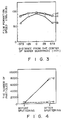
- the film formation speed is set to 80 nm/min, and the uniformity of the speed of sputtering for the substrate is detected to vary within a range of ⁇ 40% as shown by curve b in Fig. 3.
- the film formation speed and the uniformity of sputtering speed are set to 95 nm/min and ⁇ 5% as shown by curve a in Fig. 3.
- good uniformity can be obtained.
- 25 semiconductor substrates 18 are subjected to the film formation process for 10 minutes for each substrate in the same condition as described before without using protection plate 21. Then, another substrate 18 is horizontally carried in a reduced-pressure Ar atmosphere without effecting the film formation process. A particle check is effected thereafter. As shown by points d in Fig. 4, it is understood that approx. 8000 particles of 0.3 ⁇ m or more in diameter are attached to last substrate 18 as dust. The number is relatively large when considering that it was 60 before the film formation was effected. This is mainly because the sputtering film formed on chamber wall 11 is peeled off by temperature variation.
- An object of this invention is to provide a sputtering chamber structure which can prevent sputtering particles from being dispersed to various places other than a substrate without affecting uniformity in the thickness of a film formed by the high frequency bias sputtering process.
- a sputtering chamber structure comprising: first and second electrodes to which the target and semiconductor substrate are attached, respectively; a protection plate formed to surround the target and having a first opening section facing the front surface of the target and a second opening section which is formed separately from the first opening section to decentralize a target power in the inner space defined by the protection plate when the high-frequency bias sputtering process is effected in a state that the first opening section is closed by the second electrode; and a chamber for receiving the first and second electrode and the protection plate and set in a reduced-pressure condition in the high-frequency bias sputtering process.
- plasma can pass out via the second opening. Since the second opening is formed separately from the first opening, plasma will not be concentrated at or near the edge portion of the semiconductor wafer substrate. Further, particles can be prevented from falling from the top wall of the chamber down to the semiconductor wafer substrate by forming the second opening in a suitable position, for example, in a position below the protection plate.
- sputtering chamber structure of a high-frequency bias sputtering device according to one embodiment of this invention with reference to Fig. 5.
- portions which are the same as those of the conventional sputtering device are denoted by the same reference numerals.
- the sputtering device includes chamber wall 11, target flange 12 and backing plate or target electrode 13, and space defined by these elements is used as sputtering chamber SR.
- Target 14 is mounted on backing plate 13 and kept substantially vertical.
- Target earth shield 15 is mounted along the periphery of target 14.
- the sputtering device further includes groove 20 formed in the bottom portion of chamber SR, O-ring 19 provided between chamber 11 and flange 12 and domed metal protection plate 32 removably attached to target earth shield 15.
- a vacuum pump (not shown) is communicated with groove 20.
- O-ring 19 is used to keep the pressure in sputtering chamber 11 to a preset vacuum pressure.
- Target 14 is surrounded substantially entirely by metal protection plate 32.
- Protection plate 32 has opening 31 formed to face target 14 and opening 33 formed below target 14 and separately from opening 31. Opening 31 is formed to have a diameter slightly larger than semiconductor wafer substrate 18, and opening 33 is formed to have a diameter smaller than that of opening 31. Opening 31 is closed by substrate electrode 17 on which semiconductor wafer substrate 18 is put. Opening 33 is so formed that plasma can pass out from the space defined between substrate 18 and target 14 via opening 33, thus decentralizing the target power.
- stepped portion 34 is formed on electrode 17 to lap over the edge portion of protection plate 32.
- target power decentralizing opening 331 is formed in a crooked configuration so as to prevent sputtering particles from being scattered to the outer spacing via opening 331. That is, a curved gap is formed in the mounting portion of protection plate 321. Plasma may be discharged via the gap to the exterior, but sputtering particles which tend to move straightly will be prevented from being discharged via the gap to the exterior.
- protection plate 322 is mounted on chamber wall 11 and thus formed in the form of partition wall.
- protection plate 323 is mounted on chamber wall 11 and thus formed in the form of partition wall. Further, a plurality of target power decentralizing openings 333 are formed in different positions.
- a high-frequency bias sputtering device was used with domed protection plate 32 fixed on target earth shield 15 to empirically form a film.
- target 14 and substrate 18 were disposed to face each other and set at an inclination angle of 3° with respect to the vertical plane at the time of film formation, the distance between target 14 and substrate 18 was set at 60 mm, the target material was high purity quartz, the target diameter was set at 250 mm, and the diameter of substrate electrode 17 was set at 160 mm.
- the inner diameter of protection plate 32 was set at 250 mm, the height was set at 60 mm, the diameter of the opening on the wafer substrate side was set at 170 mm, and stepped portion 34 was formed on the periphery of substrate electrode 17 to cover the gap formed between protection plate 32 and substrate electrode 17 (Fig. 5).
- the diameter of opening 33 was 10 mm ⁇ 100 mm, and opening 33 was formed below protection plate 32.
- groove 20 with the width of 60 mm was formed in the bottom portion of the sputtering chamber, and groove 20 was connected to a vacuum pump (not shown).
- the film formation process was effected for 25 pieces of wafer substrates 18 of 5 inches in a condition that Ar gas was introduced into the sputtering chamber after the pressure thereof was reduced to 1.0 ⁇ 10 ⁇ 4 pa, and then Ar partial pressure was set at 0.30 pa, Ar flow rate was set at 30 SCCM, the target power was set at 3.0 kW, the substrate power was set at 0.5 kW (with the use of a permanent magnet), and the sputtering time was set at 10 minutes.
- the target power decentralizing opening of protection plate 32 may be formed in an overlapped form as shown by opening 331 in Fig. 6. In this case, plasma may pass out via opening 331, but substantially the same effect can be obtained.
- the protection plate is formed in the form of a partition plate as shown by protection plates 322 and 323 in Figs. 7 and 8, the same effect can be obtained.
- a plurality of target power decentralizing openings 333 are provided as shown in Fig. 8, but if they are provided approx. 40 mm apart from wafer 18, the distribution of the film formation speed in the substrate will not be lowered by increase in the speed of sputter-etching for local portion of the insulation film on the substrate.
- the second opening is formed in the protection plate and the peripheral portion of the protection plate defining the first opening is partly overlapped on the outer peripheral portion of the substrate electrode so that plasma can be prevented from being leaked out via the gap between the substrate electrode and the protection plate. Therefore, the sputtering speed can be made uniform, permitting an insulation film to be formed with an uniform thickness on the entire portion of the substrate. Further, since sputtering particles can be reliably blocked by means of the protection plate, they will not be attached to the inner wall of the sputtering chamber. Thus, occurrence of particles due to peel-off or separation of a film formed on the inner wall of the sputtering chamber can be prevented.
- the insulation film can be formed on any part inside the space defined by the protection plate, and the sputtering film thus formed can be prevented from being peeled off by adequately selecting the material of the protection plate surface and the electrode surface.
- the electrode surface and the protection plate can be formed of quartz (SiO2) for this purpose.
- the protection plate can be replaced, the maintenance therefor can be easily effected in comparison with the operation of cleaning the inner wall of the sputtering chamber.
Landscapes
- Chemical & Material Sciences (AREA)
- Engineering & Computer Science (AREA)
- Metallurgy (AREA)
- Organic Chemistry (AREA)
- Chemical Kinetics & Catalysis (AREA)
- Materials Engineering (AREA)
- Mechanical Engineering (AREA)
- Physics & Mathematics (AREA)
- Analytical Chemistry (AREA)
- Plasma & Fusion (AREA)
- Condensed Matter Physics & Semiconductors (AREA)
- General Physics & Mathematics (AREA)
- Manufacturing & Machinery (AREA)
- Computer Hardware Design (AREA)
- Microelectronics & Electronic Packaging (AREA)
- Power Engineering (AREA)
- Physical Vapour Deposition (AREA)
- Physical Deposition Of Substances That Are Components Of Semiconductor Devices (AREA)
Applications Claiming Priority (2)
| Application Number | Priority Date | Filing Date | Title |
|---|---|---|---|
| JP62211607A JPS6454733A (en) | 1987-08-26 | 1987-08-26 | Production device for semiconductor |
| JP211607/87 | 1987-08-26 |
Publications (3)
| Publication Number | Publication Date |
|---|---|
| EP0304895A2 true EP0304895A2 (fr) | 1989-03-01 |
| EP0304895A3 EP0304895A3 (en) | 1990-09-26 |
| EP0304895B1 EP0304895B1 (fr) | 1993-10-20 |
Family
ID=16608563
Family Applications (1)
| Application Number | Title | Priority Date | Filing Date |
|---|---|---|---|
| EP88113798A Expired - Lifetime EP0304895B1 (fr) | 1987-08-26 | 1988-08-24 | Structure d'une chambre de pulvérisation cathodique pour pulvérisation cathodique en utilisant des hautes fréquences |
Country Status (5)
| Country | Link |
|---|---|
| US (1) | US4897172A (fr) |
| EP (1) | EP0304895B1 (fr) |
| JP (1) | JPS6454733A (fr) |
| KR (1) | KR910009317B1 (fr) |
| DE (1) | DE3885043T2 (fr) |
Cited By (3)
| Publication number | Priority date | Publication date | Assignee | Title |
|---|---|---|---|---|
| EP0607786A2 (fr) * | 1993-01-19 | 1994-07-27 | Leybold Aktiengesellschaft | Appareillage pour le revêtement de substrats |
| EP0446657B1 (fr) * | 1990-03-02 | 1995-07-26 | Applied Materials, Inc. | Méthode de préparation d'un écran pour limiter les particules dans une chambre de dépôt physique en phase vapeur |
| WO2005087972A1 (fr) | 2004-03-12 | 2005-09-22 | Shinmaywa Industries, Ltd. | Appareil filmogene |
Families Citing this family (10)
| Publication number | Priority date | Publication date | Assignee | Title |
|---|---|---|---|---|
| JPH07110991B2 (ja) * | 1989-10-02 | 1995-11-29 | 株式会社日立製作所 | プラズマ処理装置およびプラズマ処理方法 |
| JP3076367B2 (ja) * | 1990-11-29 | 2000-08-14 | キヤノン株式会社 | プラズマ処理装置 |
| WO1992016671A1 (fr) * | 1991-03-20 | 1992-10-01 | Canon Kabushiki Kaisha | Procede et dispositif de formation d'une couche mince par pulverisation |
| US5736021A (en) * | 1996-07-10 | 1998-04-07 | Applied Materials, Inc. | Electrically floating shield in a plasma reactor |
| DE19755837A1 (de) * | 1997-12-16 | 1999-06-17 | Leybold Ag | Sputteranlage |
| JP4656697B2 (ja) | 2000-06-16 | 2011-03-23 | キヤノンアネルバ株式会社 | 高周波スパッタリング装置 |
| JP3972558B2 (ja) * | 2000-06-23 | 2007-09-05 | 松下電器産業株式会社 | スパッタリング装置 |
| KR100620194B1 (ko) * | 2002-12-30 | 2006-09-01 | 동부일렉트로닉스 주식회사 | 스퍼터링 장치의 공정 챔버 |
| JP2012509140A (ja) * | 2008-11-20 | 2012-04-19 | カーディアック ペースメイカーズ, インコーポレイテッド | 構造化された表面を有する細胞反発性電極 |
| KR101904516B1 (ko) * | 2011-02-09 | 2018-10-04 | 어플라이드 머티어리얼스, 인코포레이티드 | Rf pvd 챔버를 위한 균일성 튜닝 가능한 정전척 접지 키트 |
Citations (1)
| Publication number | Priority date | Publication date | Assignee | Title |
|---|---|---|---|---|
| US3730873A (en) * | 1970-03-18 | 1973-05-01 | Philips Corp | Cathode sputtering etching device with movable guard ring |
Family Cites Families (11)
| Publication number | Priority date | Publication date | Assignee | Title |
|---|---|---|---|---|
| GB1163496A (en) * | 1967-06-23 | 1969-09-04 | Edwards High Vacuum Interation | Improvements in or relating to Radio Frequency Sputtering |
| FR2324755A1 (fr) * | 1975-09-19 | 1977-04-15 | Anvar | Dispositif de pulverisation cathodique de grande vitesse de depot |
| JPS5621836A (en) * | 1979-07-31 | 1981-02-28 | Makoto Ishikawa | Manufacture of polyvinyl chloride made hollow ball |
| US4525262A (en) * | 1982-01-26 | 1985-06-25 | Materials Research Corporation | Magnetron reactive bias sputtering method and apparatus |
| JPS58151547A (ja) * | 1982-03-05 | 1983-09-08 | Shinkosumosu Denki Kk | 電力帰還型ガス検知装置 |
| JPS58164228A (ja) * | 1982-03-25 | 1983-09-29 | Toshiba Corp | 誘電体の薄膜形成方法 |
| JPS5917236A (ja) * | 1982-07-21 | 1984-01-28 | Hitachi Ltd | 膜形成装置 |
| JPS6026659A (ja) * | 1983-07-25 | 1985-02-09 | Anelva Corp | スパツタリング装置 |
| JPS60197873A (ja) * | 1984-03-19 | 1985-10-07 | Ulvac Corp | スパツタリング装置における絶縁物タ−ゲツト用ア−スシ−ルド装置 |
| JPS62284074A (ja) * | 1985-12-27 | 1987-12-09 | Arubatsuku Seimaku Kk | 連続スパツタリング装置 |
| JPS62167876A (ja) * | 1986-01-20 | 1987-07-24 | Meidensha Electric Mfg Co Ltd | スパツタリング装置 |
-
1987
- 1987-08-26 JP JP62211607A patent/JPS6454733A/ja active Pending
-
1988
- 1988-08-24 US US07/236,384 patent/US4897172A/en not_active Expired - Lifetime
- 1988-08-24 EP EP88113798A patent/EP0304895B1/fr not_active Expired - Lifetime
- 1988-08-24 KR KR1019880010740A patent/KR910009317B1/ko not_active IP Right Cessation
- 1988-08-24 DE DE88113798T patent/DE3885043T2/de not_active Expired - Lifetime
Patent Citations (1)
| Publication number | Priority date | Publication date | Assignee | Title |
|---|---|---|---|---|
| US3730873A (en) * | 1970-03-18 | 1973-05-01 | Philips Corp | Cathode sputtering etching device with movable guard ring |
Non-Patent Citations (1)
| Title |
|---|
| PATENT ABSTRACTS OF JAPAN, unexamined applications, E section, vol. 8, no. 194, September 6, 1984 THE PATENT OFFICE JAPANESE GOVERNMENT page 11 E 264 * |
Cited By (6)
| Publication number | Priority date | Publication date | Assignee | Title |
|---|---|---|---|---|
| EP0446657B1 (fr) * | 1990-03-02 | 1995-07-26 | Applied Materials, Inc. | Méthode de préparation d'un écran pour limiter les particules dans une chambre de dépôt physique en phase vapeur |
| EP0607786A2 (fr) * | 1993-01-19 | 1994-07-27 | Leybold Aktiengesellschaft | Appareillage pour le revêtement de substrats |
| EP0607786A3 (fr) * | 1993-01-19 | 1995-03-22 | Leybold Ag | Appareillage pour le revêtement de substrats. |
| WO2005087972A1 (fr) | 2004-03-12 | 2005-09-22 | Shinmaywa Industries, Ltd. | Appareil filmogene |
| EP1752558A1 (fr) * | 2004-03-12 | 2007-02-14 | Shinmaywa Industries, Ltd. | Appareil filmogene |
| EP1752558A4 (fr) * | 2004-03-12 | 2008-07-30 | Shinmaywa Ind Ltd | Appareil filmogene |
Also Published As
| Publication number | Publication date |
|---|---|
| DE3885043D1 (de) | 1993-11-25 |
| KR910009317B1 (ko) | 1991-11-09 |
| US4897172A (en) | 1990-01-30 |
| KR890004417A (ko) | 1989-04-21 |
| DE3885043T2 (de) | 1994-02-10 |
| JPS6454733A (en) | 1989-03-02 |
| EP0304895B1 (fr) | 1993-10-20 |
| EP0304895A3 (en) | 1990-09-26 |
Similar Documents
| Publication | Publication Date | Title |
|---|---|---|
| US5985102A (en) | Kit for electrically isolating collimator of PVD chamber, chamber so modified, and method of using | |
| EP0304895B1 (fr) | Structure d'une chambre de pulvérisation cathodique pour pulvérisation cathodique en utilisant des hautes fréquences | |
| US4871433A (en) | Method and apparatus for improving the uniformity ion bombardment in a magnetron sputtering system | |
| KR100659828B1 (ko) | 이온화 물리적 증착 방법 및 장치 | |
| US5213650A (en) | Apparatus for removing deposits from backside and end edge of semiconductor wafer while preventing removal of materials from front surface of wafer | |
| JP3775689B2 (ja) | 材料をイオン化スパッタリングする方法と装置 | |
| US5075256A (en) | Process for removing deposits from backside and end edge of semiconductor wafer while preventing removal of materials from front surface of wafer | |
| US5948215A (en) | Method and apparatus for ionized sputtering | |
| US5384008A (en) | Process and apparatus for full wafer deposition | |
| US6416634B1 (en) | Method and apparatus for reducing target arcing during sputter deposition | |
| KR100328134B1 (ko) | 스퍼터링율의균등성을증가시키기위한스퍼터증착장치및방법 | |
| US20090294063A1 (en) | Plasma processing apparatus | |
| US7338578B2 (en) | Step edge insert ring for etch chamber | |
| JP2000144399A (ja) | スパッタリング装置 | |
| KR100284248B1 (ko) | 스퍼터링장치 | |
| KR100255532B1 (ko) | 고 종횡비의 컨택트 홀내에 전도성막을 형성하기 위한 스퍼터링 장치 | |
| JPS627852A (ja) | 薄膜形成方法 | |
| US6521106B1 (en) | Collimated deposition apparatus | |
| TWI801632B (zh) | 用於電漿處理腔室的處理套件、用於rfpvd腔室的處理套件、及pvd腔室 | |
| JPH07221019A (ja) | 平行化付着装置 | |
| US20170178875A1 (en) | Insulator target | |
| KR19990028451A (ko) | 고종횡비의등각라이너박막및플러그들의개선된증착을위한장치및방법 | |
| JP2003073801A (ja) | スパッタ装置およびその方法 | |
| KR20010039233A (ko) | 반도체 스퍼터링 설비의 웨이퍼 에칭 장치 | |
| JPH10204634A (ja) | マグネトロンカソードおよびこれを備えたメタル配線スパッタ装置 |
Legal Events
| Date | Code | Title | Description |
|---|---|---|---|
| PUAI | Public reference made under article 153(3) epc to a published international application that has entered the european phase |
Free format text: ORIGINAL CODE: 0009012 |
|
| 17P | Request for examination filed |
Effective date: 19880921 |
|
| AK | Designated contracting states |
Kind code of ref document: A2 Designated state(s): DE FR GB |
|
| PUAL | Search report despatched |
Free format text: ORIGINAL CODE: 0009013 |
|
| AK | Designated contracting states |
Kind code of ref document: A3 Designated state(s): DE FR GB |
|
| 17Q | First examination report despatched |
Effective date: 19920722 |
|
| GRAA | (expected) grant |
Free format text: ORIGINAL CODE: 0009210 |
|
| AK | Designated contracting states |
Kind code of ref document: B1 Designated state(s): DE FR GB |
|
| REF | Corresponds to: |
Ref document number: 3885043 Country of ref document: DE Date of ref document: 19931125 |
|
| ET | Fr: translation filed | ||
| PLBE | No opposition filed within time limit |
Free format text: ORIGINAL CODE: 0009261 |
|
| STAA | Information on the status of an ep patent application or granted ep patent |
Free format text: STATUS: NO OPPOSITION FILED WITHIN TIME LIMIT |
|
| 26N | No opposition filed | ||
| REG | Reference to a national code |
Ref country code: GB Ref legal event code: 746 Effective date: 19981026 |
|
| REG | Reference to a national code |
Ref country code: FR Ref legal event code: D6 |
|
| REG | Reference to a national code |
Ref country code: GB Ref legal event code: IF02 |
|
| PGFP | Annual fee paid to national office [announced via postgrant information from national office to epo] |
Ref country code: DE Payment date: 20070816 Year of fee payment: 20 |
|
| PGFP | Annual fee paid to national office [announced via postgrant information from national office to epo] |
Ref country code: GB Payment date: 20070822 Year of fee payment: 20 |
|
| PGFP | Annual fee paid to national office [announced via postgrant information from national office to epo] |
Ref country code: FR Payment date: 20070808 Year of fee payment: 20 |
|
| REG | Reference to a national code |
Ref country code: GB Ref legal event code: PE20 Expiry date: 20080823 |
|
| PG25 | Lapsed in a contracting state [announced via postgrant information from national office to epo] |
Ref country code: GB Free format text: LAPSE BECAUSE OF EXPIRATION OF PROTECTION Effective date: 20080823 |