EP0302002B1 - Procédé de conversion d'un signal d'entrée analogique en un signal de sortie numérique - Google Patents
Procédé de conversion d'un signal d'entrée analogique en un signal de sortie numérique Download PDFInfo
- Publication number
- EP0302002B1 EP0302002B1 EP88730153A EP88730153A EP0302002B1 EP 0302002 B1 EP0302002 B1 EP 0302002B1 EP 88730153 A EP88730153 A EP 88730153A EP 88730153 A EP88730153 A EP 88730153A EP 0302002 B1 EP0302002 B1 EP 0302002B1
- Authority
- EP
- European Patent Office
- Prior art keywords
- converter
- microcomputer
- signal
- capacitor
- internal
- Prior art date
- Legal status (The legal status is an assumption and is not a legal conclusion. Google has not performed a legal analysis and makes no representation as to the accuracy of the status listed.)
- Expired - Lifetime
Links
- 238000000034 method Methods 0.000 title claims description 26
- 239000003990 capacitor Substances 0.000 claims description 39
- 238000006243 chemical reaction Methods 0.000 description 8
- 230000003321 amplification Effects 0.000 description 7
- 238000003199 nucleic acid amplification method Methods 0.000 description 7
- 239000008186 active pharmaceutical agent Substances 0.000 description 5
- 238000005259 measurement Methods 0.000 description 4
- 108010014172 Factor V Proteins 0.000 description 2
- 238000004364 calculation method Methods 0.000 description 2
- 238000013213 extrapolation Methods 0.000 description 2
- 230000015572 biosynthetic process Effects 0.000 description 1
- 230000001419 dependent effect Effects 0.000 description 1
- 230000000694 effects Effects 0.000 description 1
- 230000002349 favourable effect Effects 0.000 description 1
- 230000007774 longterm Effects 0.000 description 1
- 230000002123 temporal effect Effects 0.000 description 1
Images
Classifications
-
- H—ELECTRICITY
- H03—ELECTRONIC CIRCUITRY
- H03M—CODING; DECODING; CODE CONVERSION IN GENERAL
- H03M1/00—Analogue/digital conversion; Digital/analogue conversion
- H03M1/12—Analogue/digital converters
- H03M1/14—Conversion in steps with each step involving the same or a different conversion means and delivering more than one bit
- H03M1/16—Conversion in steps with each step involving the same or a different conversion means and delivering more than one bit with scale factor modification, i.e. by changing the amplification between the steps
-
- H—ELECTRICITY
- H03—ELECTRONIC CIRCUITRY
- H03M—CODING; DECODING; CODE CONVERSION IN GENERAL
- H03M1/00—Analogue/digital conversion; Digital/analogue conversion
- H03M1/66—Digital/analogue converters
- H03M1/82—Digital/analogue converters with intermediate conversion to time interval
Definitions
- the invention relates to a method for converting an analog input signal into a digital output signal, in which a digital signal of an internal A / D converter to which the input signal is applied is fed back via a microcomputer and via a D / A converter arranged downstream thereof converted by the microcomputer on the digital signal of the internal A / D converter output signal into an analog signal which is fed back to the internal A / D converter via a differential amplifier fed by the analog input signal.
- the output signal of the Microcomputers determined by extrapolation algorithms by, for example, for a value of the analog input signal sampled at a time t x - based on the corresponding digital signal of the internal A / D converter - from the double value of the digital output signal at time t x - 1 the value of digital output signal at time t x - 2 is subtracted.
- a "digital prediction" is thus made for the sample value of the input signal to be implemented at the time t x from the digital output values at the past times t x-1 and tx-2, which, however, is then correspondingly formed by forming a difference to the analog input signal must be corrected at time t x .
- the digital prediction must be relatively accurate. As a prerequisite for the application of such a method using extrapolation algorithms, the most uniform and, above all, sinusoidal course of the analog input signal must be present.
- the method according to the invention makes use of a simple capacitor, in which the charging takes place as a function of the single or multiple times of the high-precision control cycle time of the microcomputer. If the capacitor is charged by the switching signal, which controls a switch connected to a constant voltage source, for example, during an extremely precisely determined charging time from the constant voltage source via a resistor, its charging voltage, which represents the analog output signal of the D / A converter, has then reaches a predetermined value with the same accuracy.
- an accuracy can thus be achieved which is within the range of the desired overall accuracy of the implementation method (14 to 16 bit).
- a major advantage is that any temporal courses of the input signal can be processed with the method according to the invention, because the switching signal is formed via the output signal of the microcomputer directly as a function of the current digital signal from the internal A / D converter. It is thus formed for the current sample value of the input variable to be converted; "Predictions" are dropped.
- the dependence of the formation of the switching signal on the digital signal of the internal A / D converter is given by a comparison carried out by the microcomputer of the current input voltage corresponding to the analog input signal with the capacitor charging voltage to be generated in such a way that the amplified difference between the current input voltage and the capacitor charging voltage always lies exactly in the implementation area of the internal A / D converter. If, for example, it processes only positive difference signals as input signals, the microcomputer carries out the comparison in such a way that the capacitor voltage is the somewhat higher voltage. This ensures in this case that the method according to the invention normally always delivers a digital output signal, since the difference to be formed when the capacitor charging voltage is applied to the positive input of the differential amplifier is always greater than zero.
- the charged capacitor is discharged by the microcomputer in a predetermined measuring cycle. In this way it can be ensured in a simple manner via the microcomputer that the capacitor is after one Implementation run of loaded cargo is also discharged again so that it is ready for the next implementation run.
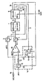
- the method according to the invention for converting an analog input signal into a digital output signal is explained in more detail below with reference to the figure.
- the figure shows the basic structure of a preferred circuit arrangement for carrying out the method according to the invention.
- an internal A / D converter 1 is shown, the input 2 of which is connected to a first switch 3 and a second switch 4.
- a microcomputer 6 is connected to an output 5 of the internal A / D converter 1.
- This microcomputer 6 has a first control line 7, via which it can control a further switch 8.
- This further switch 8 is connected to ground potential with its output 9 and connected in parallel with a capacitor 11 with its input 10.
- a resistor 12 is arranged in series with this capacitor 11, to which an additional switch 13 is in turn connected.
- This additional switch 13 is connected with its one output to a constant voltage source UK.
- the capacitor 11, the further switch 8 and the additional switch 13 and the resistor 12 together form a D / A converter 14.
- the capacitor 11 is connected to a positive input of a differential amplifier 15, the negative input of which is supplied with an analog input signal AES, which is applied to an input 16, and the output of which is connected to the second switch 4.
- the microcomputer 6 also has a second control line 17, via which the first switch 3 can be controlled, a third control line 18, via which the second switch 4 can be controlled, and a fourth control line 19 with which the Microcomputer 6 can control the additional switch 13.
- the microcomputer 6 has an indicating output 20, at which a determined digital output signal DAS can be displayed.
- the sequence of a conversion run which determines the measuring cycle of the implementation process, according to the inventive method is described below.
- the input signal AES which may be sampled by a sample and hold element, not shown, and which is given to input 16 and corresponds to an input voltage UE, is - in addition to its permanent line to the negative input of differential amplifier 15 - from microcomputer 6 to input 2 of internal A / D converter 1 given by the microcomputer 6 causes the first switch 3 to close via its second control line 17.
- the internal A / D converter 1 is, for example, an 8 bit converter and digitizes the input signal AES with the appropriate resolution.
- a digital signal DS generated in this way from the internal A / D converter 1 (shown in the figure in the upper part of the internal A / D converter 1) is then fed back through the following circuit arrangement.
- Feedback is a process-specific property. It has the effect that the "rough" conversion initially carried out in the internal A / D converter 1 is refined, i. H. the number of bits displayed is increased by detecting the as yet undetected fine area lying below the "coarse" bit initially displayed, which is not yet detected, by forming a difference to a corresponding analog input signal and spreading it accordingly by amplification. The subsequent digitization in the internal A / D converter 1 then essentially results in the "fine conversion", the bit number of which is simply “appended” to the "rough” bit number. Any overlap of the coarse and fine conversion that may occur is determined by an amplification factor V of the differential amplifier 15.
- the digital signal DS of the internal A / D converter 1 is first passed to the microcomputer 6.
- the task of the microcomputer 6 is u. a.
- To generate an output signal AS which is based on the digital signal DS of the internal A / D converter 1.
- a table is stored in the microcomputer 6, for example, in which digitized values of a capacitor charging voltage UC of the capacitor 11 are stored with the associated charging times.
- the loading times are chosen so that they are one or more times the constant control cycle time of the microcomputer 6; accordingly, the individual charge voltage stages UC of the capacitor 11 are discretized.
- the microprocessor 6 - in the exemplary embodiment described - now searches for the digitized value of the capacitor charging voltage UC in its table which is somewhat larger than the digital signal DS, and takes the associated charging time from the table .
- the process of comparing the tables to determine the charging time can of course also be carried out by calculation using the formula for the capacitor charging voltage.
- it is an advantage of the table that the non-linearity when charging the capacitor 11 can be taken into account quickly, with small changes in the time constant (product of the resistor 12 and the capacitance of the capacitor 11) not causing large non-linearity errors.
- the discrete value of the charging time forms the output signal AS of the microcomputer 6, with which the latter then controls the additional switch 13 via the fourth control line 19.
- the additional switch 13 receives the output signal AS as a switching signal SS and closes for the duration of the selected charging time.
- the capacitor 11 is charged via the resistor 12 from the constant voltage source UK. Since the charging time of the capacitor 11 is one or more times the constant control cycle time of the microcomputer 6 and the latter can thus control the charging time of the capacitor 11 with high precision, it is ensured that the con capacitor-adjusting capacitor charging voltage UC is achieved with the same precision.
- the D / A converter 14 containing the capacitor 11 can be an 8-bit converter, which therefore has the same resolution as the internal A / D converter 1.
- the individual discrete charging voltage values UC of the capacitor 11 can for example with a 16 bit accuracy, i. H. to 16 exact digits can be set if they are stored as 16 bit numbers in the table of the microcomputer 6 or if they are calculated with 16 bit digits.
- the additional switch 13 is caused to open by the microcomputer 6, and the capacitor 11 has a capacitor charging voltage UC, which is determined with 16 bits and which was selected by the microcomputer 6 in such a way that it is somewhat larger than that corresponding voltage value UE of the sampled analog input signal AES.
- the capacitor charging voltage UC is then passed to the positive input of the differential amplifier 15, and since this has its negative input applied to the sample value of the analog input signal AES, it forms a positive voltage difference between the two.
- This amplification factor corresponds to a resolution of 2 7 bits, with which the differential amplifier 15 spreads or spreads out the voltage difference formed accordingly.
- the microcomputer 6 then controls the second switch 4 via the third control line 18, so that it closes briefly and the amplified voltage difference A U, after it has stabilized after a corresponding waiting time, is again fed to the internal A / D converter 1.
- the internal A / D converter 1 has, for example, the resolution of 8 bits, so that the amplified voltage difference A U of the differential amplifier 15 fanned out to 7 bits is resolved again with 8 bits, so that the conversion method has an overall accuracy of 15 bits.
- the 8 bit accuracy of the internal A / D converter 1 is overlapped with the 8 bit accuracy of the D / A converter 14 in accordance with the amplification factor V with 7 bits in exactly one bit, so that the overall accuracy of 15 bits arises.
- the microcomputer 6 After determining the digital output signal DAS, the microcomputer 6 then drives the further switch 8 via the first control line 7, so that it closes and the capacitor 11 is discharged. The further switch 8 then opens again, and the entire circuit arrangement is in the standby position for the next implementation process, in accordance with the measuring cycle.
- a microcomputer 6 can also be used, which provides the analog input signal AES and the amplified voltage difference A U to an integrated A / D converter 1 via a multiplexer input feeds.
- the microcomputer 6 can have a counter with comparison registers.
- the method according to the invention can be used to carry out reference measurements with a maximum voltage and with zero potential. It is sufficient to alternately carry out one of the two reference measurements after each measurement.
- the switching between the individual input signals can also be controlled by the microcomputer 6 in the measuring cycle.
- a loop for recharging the capacitor 11 can also be built into the program for the microcomputer 6 for passing through a measurement cycle in the event that 15 values for the amplified voltage difference A U occur at the output of the differential amplifier that are not determined by the internal A / D-converter 1 can be implemented.
Landscapes
- Engineering & Computer Science (AREA)
- Theoretical Computer Science (AREA)
- Analogue/Digital Conversion (AREA)
- Measurement Of Resistance Or Impedance (AREA)
Claims (2)
Applications Claiming Priority (2)
| Application Number | Priority Date | Filing Date | Title |
|---|---|---|---|
| DE3725875 | 1987-07-30 | ||
| DE19873725875 DE3725875A1 (de) | 1987-07-30 | 1987-07-30 | Verfahren zum umsetzen eines analogen eingangssignals in ein digitales ausgangssignal |
Publications (2)
| Publication Number | Publication Date |
|---|---|
| EP0302002A1 EP0302002A1 (fr) | 1989-02-01 |
| EP0302002B1 true EP0302002B1 (fr) | 1990-12-27 |
Family
ID=6333047
Family Applications (1)
| Application Number | Title | Priority Date | Filing Date |
|---|---|---|---|
| EP88730153A Expired - Lifetime EP0302002B1 (fr) | 1987-07-30 | 1988-07-05 | Procédé de conversion d'un signal d'entrée analogique en un signal de sortie numérique |
Country Status (2)
| Country | Link |
|---|---|
| EP (1) | EP0302002B1 (fr) |
| DE (2) | DE3725875A1 (fr) |
Families Citing this family (3)
| Publication number | Priority date | Publication date | Assignee | Title |
|---|---|---|---|---|
| DE4125717C1 (en) * | 1991-08-02 | 1993-02-11 | Robert Dipl.-Ing. 8028 Taufkirchen De Westendorp | Correcting or calibrating characteristic curve of sequentially working A=D converter - addressing correction value stored in ROM for each digital internal state of converter |
| DE4312697A1 (de) * | 1993-04-20 | 1994-10-27 | Leybold Ag | Vorrichtung zum Digitalisieren einer Analogspannung |
| CN108020339A (zh) * | 2017-12-25 | 2018-05-11 | 广州市熙泰自控设备有限公司 | 一种免输入标定的热电阻测量电路 |
-
1987
- 1987-07-30 DE DE19873725875 patent/DE3725875A1/de not_active Withdrawn
-
1988
- 1988-07-05 DE DE8888730153T patent/DE3861440D1/de not_active Expired - Lifetime
- 1988-07-05 EP EP88730153A patent/EP0302002B1/fr not_active Expired - Lifetime
Also Published As
| Publication number | Publication date |
|---|---|
| EP0302002A1 (fr) | 1989-02-01 |
| DE3861440D1 (de) | 1991-02-07 |
| DE3725875A1 (de) | 1989-02-09 |
Similar Documents
| Publication | Publication Date | Title |
|---|---|---|
| DE1259462B (de) | Einrichtung zur digitalen Anzeige einer analogen Eingangsspannung | |
| DE4307021A1 (fr) | ||
| CH665027A5 (de) | Verfahren zur messung und digitalisierung eines widerstandes und schaltung zur durchfuehrung des verfahrens. | |
| DE2923026C2 (de) | Verfahren zur Analog/Digital-Umsetzung und Anordnung zur Durchführung des Verfahrens | |
| DE1288632B (de) | Analog/Digital-Umsetzer mit einem Integrierverstaerker | |
| DE1905176B2 (de) | Verfahren zur analog-digital-umsetzung mit verbesserter differentiallinearitaet der umsetzung und anordnung zur durchfuehrung dieses verfahrens | |
| DE2614697A1 (de) | Verfahren und vorrichtung zur digitalen messung elektrischer spannungen sowie sehr geringer elektrischer widerstaende | |
| EP0302002B1 (fr) | Procédé de conversion d'un signal d'entrée analogique en un signal de sortie numérique | |
| DE3710904A1 (de) | Verfahren und anordnung zur auswertung einer analogen elektrischen messgroesse | |
| DE69219216T2 (de) | Analog-Digitalumsetzer mit erhöhter Auflösung | |
| EP0376024A2 (fr) | Procédé et dispositif de correction des tolérances de manufacture des éléments d'un circuit de traitement de signaux | |
| EP0444233B1 (fr) | Procédé et dispositif de conversion analogique/numérique d'un signal d'entrée analogique variant dans le temps | |
| DE8900990U1 (de) | Schaltungsvorrichtung mit dividierendem Analogdigitalwandler | |
| EP0444234B1 (fr) | Procédé et dispositif de conversion analogique/numérique | |
| DE19631972C2 (de) | Verfahren zum Überwachen der Funktionsfähigkeit eines zur Digitalisierung von Analogsignalen ausgelegten Analog/-Digital Wandlers | |
| DE2621087C3 (de) | Verfahren und Schaltungsanordnung zum Umwandeln einer analogen Größe in eine digitale Größe | |
| DE2547746C3 (de) | Vorrichtung zur Bildung des arithmetischen Mittelwertes einer Meßgröße | |
| DE2932371C2 (de) | Analog-Digital-Konverter mit einem Komparator zur Verarbeitung bipolarer Eingangsspannungen | |
| DE2826314A1 (de) | Analog-digital-wandler | |
| EP0456168A2 (fr) | Dispositif de conversion analogue-digitale d'un grandeur de mesure, engendré par des transducteurs disposés dans un circuit à pont, en particulier par des jauges de contrainte dans une cellule de pesage | |
| DE2308788A1 (de) | Strommessgeraet | |
| DE2935831C2 (fr) | ||
| DE2363522A1 (de) | Korrekturschaltung fuer eine schaltungsanordnung zum bearbeiten von analogsignalen | |
| DE69005469T2 (de) | Verfahren und Apparatur zur Messung von kleinen Kapazitäten. | |
| DE2331457A1 (de) | Analog-digital-umsetzer |
Legal Events
| Date | Code | Title | Description |
|---|---|---|---|
| PUAI | Public reference made under article 153(3) epc to a published international application that has entered the european phase |
Free format text: ORIGINAL CODE: 0009012 |
|
| AK | Designated contracting states |
Kind code of ref document: A1 Designated state(s): DE FR GB IT NL SE |
|
| 17P | Request for examination filed |
Effective date: 19890221 |
|
| 17Q | First examination report despatched |
Effective date: 19900227 |
|
| GRAA | (expected) grant |
Free format text: ORIGINAL CODE: 0009210 |
|
| AK | Designated contracting states |
Kind code of ref document: B1 Designated state(s): DE FR GB IT NL SE |
|
| GBT | Gb: translation of ep patent filed (gb section 77(6)(a)/1977) | ||
| REF | Corresponds to: |
Ref document number: 3861440 Country of ref document: DE Date of ref document: 19910207 |
|
| ET | Fr: translation filed | ||
| ITF | It: translation for a ep patent filed | ||
| PLBE | No opposition filed within time limit |
Free format text: ORIGINAL CODE: 0009261 |
|
| STAA | Information on the status of an ep patent application or granted ep patent |
Free format text: STATUS: NO OPPOSITION FILED WITHIN TIME LIMIT |
|
| 26N | No opposition filed | ||
| PGFP | Annual fee paid to national office [announced via postgrant information from national office to epo] |
Ref country code: GB Payment date: 19920619 Year of fee payment: 5 |
|
| PGFP | Annual fee paid to national office [announced via postgrant information from national office to epo] |
Ref country code: FR Payment date: 19920724 Year of fee payment: 5 |
|
| PGFP | Annual fee paid to national office [announced via postgrant information from national office to epo] |
Ref country code: SE Payment date: 19920728 Year of fee payment: 5 |
|
| ITTA | It: last paid annual fee | ||
| PGFP | Annual fee paid to national office [announced via postgrant information from national office to epo] |
Ref country code: NL Payment date: 19920731 Year of fee payment: 5 |
|
| PG25 | Lapsed in a contracting state [announced via postgrant information from national office to epo] |
Ref country code: GB Effective date: 19930705 |
|
| PG25 | Lapsed in a contracting state [announced via postgrant information from national office to epo] |
Ref country code: SE Effective date: 19930706 |
|
| PG25 | Lapsed in a contracting state [announced via postgrant information from national office to epo] |
Ref country code: NL Effective date: 19940201 |
|
| GBPC | Gb: european patent ceased through non-payment of renewal fee |
Effective date: 19930705 |
|
| NLV4 | Nl: lapsed or anulled due to non-payment of the annual fee | ||
| PG25 | Lapsed in a contracting state [announced via postgrant information from national office to epo] |
Ref country code: FR Effective date: 19940331 |
|
| REG | Reference to a national code |
Ref country code: FR Ref legal event code: ST |
|
| EUG | Se: european patent has lapsed |
Ref document number: 88730153.9 Effective date: 19940210 |
|
| PG25 | Lapsed in a contracting state [announced via postgrant information from national office to epo] |
Ref country code: IT Free format text: LAPSE BECAUSE OF NON-PAYMENT OF DUE FEES;WARNING: LAPSES OF ITALIAN PATENTS WITH EFFECTIVE DATE BEFORE 2007 MAY HAVE OCCURRED AT ANY TIME BEFORE 2007. THE CORRECT EFFECTIVE DATE MAY BE DIFFERENT FROM THE ONE RECORDED. Effective date: 20050705 |
|
| PGFP | Annual fee paid to national office [announced via postgrant information from national office to epo] |
Ref country code: DE Payment date: 20070919 Year of fee payment: 20 |