EP0300563B1 - Verfahren zur Herstellung von Halbleiterbauelementen wobei eine Oberfläche einer Halbleiterstruktur selektiv behandelt wird - Google Patents
Verfahren zur Herstellung von Halbleiterbauelementen wobei eine Oberfläche einer Halbleiterstruktur selektiv behandelt wird Download PDFInfo
- Publication number
- EP0300563B1 EP0300563B1 EP88201505A EP88201505A EP0300563B1 EP 0300563 B1 EP0300563 B1 EP 0300563B1 EP 88201505 A EP88201505 A EP 88201505A EP 88201505 A EP88201505 A EP 88201505A EP 0300563 B1 EP0300563 B1 EP 0300563B1
- Authority
- EP
- European Patent Office
- Prior art keywords
- layer
- solvent
- treated
- projections
- polymer composition
- Prior art date
- Legal status (The legal status is an assumption and is not a legal conclusion. Google has not performed a legal analysis and makes no representation as to the accuracy of the status listed.)
- Expired - Lifetime
Links
Images


Classifications
-
- H—ELECTRICITY
- H10—SEMICONDUCTOR DEVICES; ELECTRIC SOLID-STATE DEVICES NOT OTHERWISE PROVIDED FOR
- H10P—GENERIC PROCESSES OR APPARATUS FOR THE MANUFACTURE OR TREATMENT OF DEVICES COVERED BY CLASS H10
- H10P50/00—Etching of wafers, substrates or parts of devices
- H10P50/69—Etching of wafers, substrates or parts of devices using masks for semiconductor materials
- H10P50/691—Etching of wafers, substrates or parts of devices using masks for semiconductor materials for Group V materials or Group III-V materials
- H10P50/692—Etching of wafers, substrates or parts of devices using masks for semiconductor materials for Group V materials or Group III-V materials characterised by their composition, e.g. multilayer masks or materials
-
- H—ELECTRICITY
- H10—SEMICONDUCTOR DEVICES; ELECTRIC SOLID-STATE DEVICES NOT OTHERWISE PROVIDED FOR
- H10P—GENERIC PROCESSES OR APPARATUS FOR THE MANUFACTURE OR TREATMENT OF DEVICES COVERED BY CLASS H10
- H10P14/00—Formation of materials, e.g. in the shape of layers or pillars
- H10P14/60—Formation of materials, e.g. in the shape of layers or pillars of insulating materials
- H10P14/68—Organic materials, e.g. photoresists
- H10P14/683—Organic materials, e.g. photoresists carbon-based polymeric organic materials, e.g. polyimides, poly cyclobutene or PVC
-
- H—ELECTRICITY
- H10—SEMICONDUCTOR DEVICES; ELECTRIC SOLID-STATE DEVICES NOT OTHERWISE PROVIDED FOR
- H10P—GENERIC PROCESSES OR APPARATUS FOR THE MANUFACTURE OR TREATMENT OF DEVICES COVERED BY CLASS H10
- H10P50/00—Etching of wafers, substrates or parts of devices
- H10P50/20—Dry etching; Plasma etching; Reactive-ion etching
- H10P50/28—Dry etching; Plasma etching; Reactive-ion etching of insulating materials
- H10P50/282—Dry etching; Plasma etching; Reactive-ion etching of insulating materials of inorganic materials
- H10P50/283—Dry etching; Plasma etching; Reactive-ion etching of insulating materials of inorganic materials by chemical means
-
- H—ELECTRICITY
- H10—SEMICONDUCTOR DEVICES; ELECTRIC SOLID-STATE DEVICES NOT OTHERWISE PROVIDED FOR
- H10P—GENERIC PROCESSES OR APPARATUS FOR THE MANUFACTURE OR TREATMENT OF DEVICES COVERED BY CLASS H10
- H10P50/00—Etching of wafers, substrates or parts of devices
- H10P50/60—Wet etching
- H10P50/64—Wet etching of semiconductor materials
- H10P50/642—Chemical etching
-
- H—ELECTRICITY
- H10—SEMICONDUCTOR DEVICES; ELECTRIC SOLID-STATE DEVICES NOT OTHERWISE PROVIDED FOR
- H10P—GENERIC PROCESSES OR APPARATUS FOR THE MANUFACTURE OR TREATMENT OF DEVICES COVERED BY CLASS H10
- H10P50/00—Etching of wafers, substrates or parts of devices
- H10P50/69—Etching of wafers, substrates or parts of devices using masks for semiconductor materials
- H10P50/691—Etching of wafers, substrates or parts of devices using masks for semiconductor materials for Group V materials or Group III-V materials
Definitions
- This invention relates to the processing of semiconductor devices and circuits, and more particularly relates to a method for selectively treating surface features of a semiconductor structure above a predetermined vertical level.
- the upper layers of the devices such as the metal interconnect patterns, must accommodate more abrupt changes in surface topography caused by the smaller lateral dimensions of the devices. Deviations from planarity, sometimes called “steps”, make accurate micropatterning of the surface configuration difficult. In extreme cases, steps cannot be covered completely, so that discontinuities occur in the overlying metal layer. The problem is accentuated as more layers are added, such as in the case of interconnected multilevel integrated circuits, creating more complicated surface topographies having more and larger steps.
- U.S. patent 4,025,411 describes a process in which the non-planar surface of a semiconductor device is made planar by first applying a layer of liquid photoresist over the uneven surface, then allowing the photoresist to solidify, and finally etching the surface by a physical etching method (for example, RF sputter etching or ion milling) which removes the photoresist and the underlying material at about the same rate.
- a physical etching method for example, RF sputter etching or ion milling
- etch-resistant materials said to be suitable for the practice of the invention include the photosensitive resists conventionally used in semiconductor processing as well as suitable carbon derivatives such as picein.
- the film completely covers the smallest projections, while only covering the sides of the larger projections.
- the surface of the film is markedly uneven.
- the film is heated to near the yield point of the material (for example, 50°C to 250°C) in order to allow it to flow, thereby planarizing the surface, sealing pin holes and liberating the projections from the coating.
- the layer has receded from the sides of the larger projections (up to 100 micrometers in height) and no longer covers the smaller projections.
- the projections thus exposed are subsequently removed by a chemical etchant.
- a principal object of the invention is to provide a single step, economical process for forming a continuous, substantially planar protective layer on the surface of a semiconductor structure to be treated.
- Another object of the invention is to provide such a layer which surrounds projections from the surface of the structure so that the projections may be subsequently selectively treated.
- Another object of the invention is to provide control over the thickness of the protective layer so that only those projections above a predetermined vertical level of the structure may be selectively treated.
- a process for manufacturing semiconductor devices in which method surface features of a semiconductor structure supported on a planar substrate are selectively treated, the features lying above a predetermined vertical level in the structure, which method comprises:
- Solvent based polymer compositions suitable for use in the method of the invention are characterized by relatively small chained polymer components which are loosely crosslinked, which can be expanded by the addition of a non-polar solvent or an increase in pH, and which will relax and may, depending upon the composition and the environment, spontaneously crosslink upon evaporation of the solvent to form a cured protective layer.
- the compositions must also have sufficient fluidity prior to curing to spontaneously form a substantially planar upper surface, and have sufficient cohesiveness during relaxation and crosslinking to substantially overcome opposing forces of adhesion of the relatively thin portions of the layer adhering to the surface features to be treated, thereby drawing these portions into the surrounding bulk of the layer.
- small chained polymers as used herein is meant to include those polymers having an average molecular weight of about 72 grams/mole to 4500 grams/mole and preferably 120 grams/mole to 1200 grams/mole.
- Especially suitable polymer compositions for use in the method of the invention are solvent-soluble acrylic resin compositions, containing from about 20 to 80 volume percent of solvent, such as water soluble acrylic polymers having hydroxyl and carboxyl functional groups.
- the solvent may be polar or non-polar or a mixture of these two types, but where a non-polar solvent is relied upon to achieve swelling of the polymer, it should be present in an amount of at least about 3 volume percent.
- the expansion is thought to be necessary in order to enhance fluidity and to set up the cohesive forces required during subsequent relaxation and cross-linking to cleave the portions of the layer covering the projections and draw them into the surrounding bulk of the polymer layer, thereby exposing the projections for subsequent treatment.
- the thickness of the portions of the layer covering the projections must not exceed about 60% of the bulk thickness, and preferably be about 25% or less of the bulk thickness.
- the level of the upper surface of the solvent-expanded layer may be at or above the tops of the projections, so long as the above thickness limitations are observed.
- this surface will normally be at a lower level than the tops of the projections, in which case the solvent-expanded polymer clings to the projections without breaking the surface of the layer, by virtue of a balancing of the opposing forces of surface tension and adhesion to the surface of the projections.
- the bulk thickness of the solvent-expanded layer desired will, of course, depend upon the location of the predetermined level above which treatment will take place, and upon the amount of relaxation of the layer which will occur during drying and curing.
- the amount of relaxation i.e., volume reduction, will in general range from about 5 to 40 volume percent, depending upon the amount of solvent present and the amount of expansion which has taken place.
- An additional consideration in arriving at a desired thickness is the effect of the subsequent treatment of the projections upon the protective layer itself.
- the treatment consists of etching the projections
- certain etchants may attack and partially consume the layer during removal of the projections, depending upon the degree of resistance of the dried and cured layer. This could be advantageous in situations where progressive exposure and treatment of the projections is desired.
- the bulk thickness of the solvent-expanded layer actually obtained will depend upon its flow characteristics, which in turn are dependent upon the amount of solvent dilution and the amount of expansion, as well as upon the original flow characteristics of the undiluted polymer composition. In general, the more fluidity the composition possesses, the thinner the layer which will be obtained. Subjecting the solvent-expanded composition to sheer forces, such as the centrifugal force due to spinning of a substrate coated with the composition will enhance the flow as well as the planarization of the surface of the resultant layer.
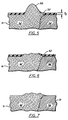
- a substrate of single crystal silicon 10 having vertical structures of various heights indicated by the letters A, B, C and D. These vertical structures may be unwanted projections from an epitaxial layer surface, vertical transistors, or other structures.
- projections A and B have been selected for treatment. Accordingly, the surface of substrate 10, including all of the projections A through D, is covered with a solvent-expanded polymer composition 11 in an amount to result in a bulk thickness T1 which is small enough after drying and curing of the layer to expose projections A and B, but large enough to form a protective covering over projections C and D.
- the thickness of the layer t1 over the tops of projections A and B should not exceed about 60% of the bulk thickness T1 and preferably not exceed about 25% of the bulk thickness T1.
- the cohesive forces of the layer, including the surface tension of the layer will in general insure that the thickness t1 will fall within the above limits.
- Fig. 4 shows the dried and cured state of the layer, now designated 12, having a bulk thickness T s and a surface 12a at a predetermined vertical level in the structure above which treatment of projections A and B will take place.
- the thickness t s of the dried and cured layer covering projection C should, of course, be sufficient to protect projection C from subsequent treatment, while the bulk thickness T s of the dried and cured layer 12 should result in the desired vertical placement of surface 12a.
- typical bulk thicknesses T s can range from about 80 nm (800 ⁇ ngström) to about 500 nm (5000 ⁇ ngström), corresponding to thicknesses T1 prior to drying and curing in the range of from about 84 nm (840 ⁇ ngström) to about 850 nm (8500 ⁇ ngström).
- t s should in general be at least about 40 nm (400 ⁇ ngström)
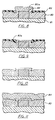
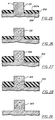
- Figs. 5 through 7 illustrate an application of the method of the invention in which the surface of a semiconductor structure is planarized by removal of so-called "bird's heads", artifacts of the formation of thick isolating oxide layers by the local oxidation of silicon.
- Fig. 5 shows such a bird's head 50 which rises above the surface of a semiconductor device 51 as an extension of field oxide region 52, by as much as about 45 nm (450 ⁇ ngström). Bird's heads disrupt the planarity of the device and interfere with subsequent metallization of the device.
- Protective layer 53 preferably having a bulk thickness T s much smaller than the height of the bird's head, is formed in the manner previously described.
- the exposed bird's head 50 is then substantially completely removed by chemical etching to result in a structure as shown in Fig. 6.
- Any of the well known chemical etchants for silicon oxide may be used, such as, for example, hydrofluoric acid, often buffered with ammonium fluoride, in which form it is commonly referred to as buffered oxide etch or "BOE".
- the protective layer 53 is then stripped away, for example, by rinsing the treated structure in the appropriate solvent for the layer 53, which may be either polar or non-polar, depending upon the nature of the polymer composition.
- a water rinse or rinsing alternately in water and a non-polar solvent such as xylene may be employed.
- the height of such bird's heads have been reduced from over 450 nm (4500 ⁇ ngström) to less than 40 nm (400 ⁇ ngström).
- both the resin and the etchant are diluted with polar solvents, or both with non-polar solvents, it is preferred to dilute either the resin or the etchant with a different miscible solvent.
- the resin is a water based acrylic polymer
- the etchant is hydrofluoric acid or BOE
- Particularly preferred for this purpose are solutions of hydrofluoric acid in isopropyl alcohol in the ratio of about 1:2 to 1:4 parts by volume, and BOE in methanol in the ratio of about 2:1 to 1:2 parts by volume.
- etching solutions have been found to result in substantial reduction of the bird's heads, for example, 100 nm (1000 ⁇ ngström ) or more, without significant undercutting of the resin layer adjacent the bird's head.
- the etchants could be diluted with other non-polar solvents, such as glycols and glycol ethers.
- the water-based acrylic polymer composition could be diluted with a non-polar solvent, or a surface modifier such as hexamethyldisilicate ("HMDS”) could be added to the polymer in order to reduce its wettability by the etchant.
- HMDS hexamethyldisilicate
- the thickness of the protective layer 53 should, of course, be sufficient to provide adequate protection of the underlying field oxide 52 and adjacent silicon mesa 54.
- the speed with which the bird's head 50 is reduced will be greater for smaller resin thicknesses, since more of the bird's head surface will be exposed to attack by the etchant, laterally as well as vertically.
- the layer thickness may be controlled by a number of factors including: polymer formulation and percent solids (both of which affect viscosity); the addition of swelling agents; the application procedure; and the drying procedure.
- the most convenient way to vary the thickness is to vary the amount of solvent dilution of the resin.
- the thickness of the layer may be varied within the range of from about 90 to 150 nm (900 to 1500 ⁇ ngström ) by varying the volume ratio of polymer to solvent within the range of about 4:1 to 1:2, with greater dilutions corresponding to lower thicknesses.
- These water-based acrylic polymers are commercially available.
- water soluble acrylic resins marketed by Röhm and Haas of Philadelphia, Pa., under the trandenames Acrysol WS-32 and Acrysol WS-50.
- a xylene-soluble acrylic polymer which has also been found suitable for use in the method of the invention is marketed by the same company under the tradename Acryloid AT-51.
- the protective polymer layer While it is unnecessary for the successful practice of the method of the invention, it may be advantageous to subject the protective polymer layer to a moderately elevated temperature during drying and curing, for example, up to 200°C, in order to accelerate drying and curing.
- a moderately elevated temperature during drying and curing, for example, up to 200°C, in order to accelerate drying and curing.
- heating may enhance adhesion of the polymer layer to the substrate. This greater adhesion may require more extensive rinsing to effect substantially complete removal of the layer from the substrate after treatment.
- alternate rinsing with different solvent types eg., water and alcohol, has been found to be more effective in removing such layers than a single rinse in one solvent.
- the water-soluble acrylic resin composition WS-50 is diluted with water to increase its initial volume one and one-half times and then diluted with methanol to increase its initial volume seven times, in order to cause expansion and increased fluidity of the polymer composition.
- Addition of the methanol also has the effect of increasing the resistance of the composition to shearing caused, for example, by the centrifugal force generated during spinning of the polymer composition onto a substrate. Such increased resistance has been found to result in better flow properties and thickness uniformity of the film.
- the protective layer 53 is then removed to result in the planarized structure shown in Fig. 7.
- Protective layer 53 may be removed simply by rinsing in a bath of one or more of the same solvents present in the diluted polymer composition.
- water based acrylate compositions it has been found that alternately rinsing in water and alcohol can remove the layer 53 more rapidly and completely than a single rinse in one of these solvents.
- the surface is dried, for example, by spinning the substrate to remove the liquid by a combination of evaporation and centrifugal force.
- a thick layer of "glass” (chemically polycrystalline silicon) 80 covering the surface of silicon substrate 81 and metal step 82 located on the substrate, is planarized.
- glass layer 80 is planarized by first forming protective polymer layer 83 in the manner already described, and then etching the portion 80a of glass layer 80 which projects above the top surface 83a of protective layer 83, to result in the planarized structure shown in Fig. 9.
- Layer 83 is then removed by solvent rinsing to result in the structure shown in Fig. 10, and a second glass layer 84 is then deposited over the first glass layer 80 to form the final structure as shown in Fig. 11.
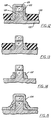
- Figs. 12 through 15 there is shown another embodiment of the invention in which vertical metal leads are defined on a vertical transistor.
- the transistor is defined by a projection 120 which rises above the surface of doped silicon substrate 122 and contains regions 124 and 126 doped with n type and p type impurities, respectively. Covering this projection is metal layer 128.
- Protective polymer layer 130 having been formed as described above, protects the portion of metal layer 128 adjacent the n-doped region of the device.
- the exposed portion of metal layer 128 is then removed by etching to result in the structure shown in Fig. 13, after which the protective polymer layer 130 is removed by rinsing to result in the structure shown in Fig. 14.
- a protective glass layer 134 is deposited over the vertical transistor 120 and vertical metal leads 132.
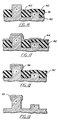
- Figs. 16 through 19 show still another embodiment of the invention in which silicon substrate 160 has two vertical projections A and B rising above the substrate surface 161, as shown in Fig. 16.
- a protective layer 162 has been formed having upper surface 163 above the upper surface of projection B but below the upper surface portion of projection A.
- Selective deposition of material on the exposed portion of projection A may then be accomplished in either of two ways.
- a layer of material 164 such as metal may be deposited over the entire surface of the structure as shown in Fig. 17, followed by stripping away protective layer 162 to result in the structure shown in Fig. 19.
- a layer of a material 166 such as a refractory metal tungstate, may be selectively deposited on the exposed silicon surface as shown in Fig. 18, and protective layer 162 then removed to result in the structure shown in Fig. 19.
- Figs. 20 through 24 show a variation of the previous embodiment in which prior to deposition of additional material on projections A and B of silicon substrate 200, projection A is first planarized with respect to projection B by the formation of protective layer 210 as shown in Fig. 20, followed by etching of projection A to result in the structure shown in Fig. 21. Protective layer 210 is then removed as shown in Fig. 22, and a new protective layer 220 is formed above the surface of projection C but below the upper portions of projections A and B, to result in the structure shown in Fig. 23. Finally, additional material 230 and 240 is deposited on projections A and B, for example, as described in connection with Figs. 16 through 19.
- Figs. 25 through 29 illustrate still another embodiment of the invention in which a vertical transistor is formed.
- Fig. 25 shows projection A from silicon substrate 300 having an exposed upper portion 301 extending above the upper surface 302a of protective polymer layer 302.
- Projection A has been previously doped, such as by solid state diffusion or ion implantation, with p-type impurities.
- Exposed portion 301 is then doped n-type, as shown in Fig. 26.
- Protective layer 302 is then replaced by a thicker protective layer 303 to expose a smaller portion 304 of projection A to doping, as shown in Fig. 27.
- This exposed portion 304 is then doped p-type, as shown in Fig. 28.
- protective layer 303 has been removed to result in a vertical pnp transistor 305.
Landscapes
- Weting (AREA)
Claims (20)
- Verfahren zur Herstellung von Halbleiteranordnungen, mit dem Oberflächenmerkmale einer Halbleiterstruktur auf einem planaren Substrat selektiv behandelt werden, wobei die Merkmale über einer vorgegebenen Ebene in der Struktur liegen, und das Verfahren folgende Schritte umfaßt:a) Bedecken der Oberfläche der Struktur einschließlich der zu behandlenden Merkmale mit einer Schicht aus einer Polymerzusammensetzung,b) Trocknen und Aushärten der Schicht bei gleichzeitigem Nachlassen und volumenmäßigem Abnehmen, um die Schicht von Oberflächenmerkmalen zurückziehen zu lassen, wodurch die Oberflächenmerkmale zur Behandlung exponiert werden,c) Behandeln der exponierten Oberflächenmerkmale, undd) Entfernen des getrockneten und ausgehärteten Films von der Oberfläche,dadurch gekennzeichnet, daß im Schritt a) die Oberfläche mit einer durchgehenden Schicht eines lösungsgedehnten, nachlaßbaren, bei Raumtemperatur aushärtenden Polymerzusammensetzung bis zu einer Ebene über der vorgegebenen Ebene um einen ausreichenden Betrag bedeckt wird, damit die obere Fläche der Schicht beim Trocknen und Aushärten bis zur vorgegebenen Ebene zurückgeht, und im Schritt b) die obere Fläche der Schicht zum Abfallen auf die vorgegebene Ebene veranlaßt wird.
- Verfahren nach Anspruch 1, dadurch gekennzeichnet, daß die Polymerzusammensetzung kleine verkettete Polymerkomponenten enthält, die lose vernetzt sind, die durch die Zugabe einer Nichtpolarlösung oder einen Anstieg des pH-Werts aufgequollen werden können und die beim Verlust der Lösung zur Bildung einer ausgehärteten Schutzschicht nachlassen.
- Verfahren nach Anspruch 2, dadurch gekennzeichnet, daß die Polymerzusammensetzung ein mittleres Molekulargewicht von 72 bis 4500 Gramm pro Mol hat.
- Verfahren nach Anspruch 3, dadurch gekennzeichnet, daß die Polymerzusammensetzung ein mittleres Molekulargewicht von 120 bis 1200 Gramm pro Mol hat.
- Verfahren nach Anspruch 1, dadurch gekennzeichnet, daß die Polymerzusammensetzung aus der Gruppe gewählt wird, die aus wasserlöslichen Acrylharzzusammensetzungen und alkohollöslichen Acrylharzzusammensetzungen sowohl mit Hydroxyl- als auch Carboxyl-Funktionsgruppen besteht.
- Verfahren nach Anspruch 5, dadurch gekennzeichnet, daß die lösungsgedehnte Polymerzusammensetzung ein Volumen von etwa dem 1- bis 10-Fachen des Ursprungsvolumens der Polymerzusammensetzung hat.
- Verfahren nach Anspruch 6, dadurch gekennzeichnet, daß die Lösung eine Mischung aus Wasser und wenigstens einer Nichtpolarlösung ist.
- Verfahren nach Anspruch 7, dadurch gekennzeichnet, daß die Nichtpolarlösung im Betrag von wenigstens 3 Volumenprozent der Gesamtlösung vorhanden ist.
- Verfahren nach Anspruch 1, dadurch gekennzeichnet, daß die Dicke der lösungsgedehnten Schicht auf den zu behandelnden Vorsprüngen bis zu etwa sechzig Prozent der Dicke der Schicht beträgt, die die zu behandelnden Vorsprünge umgibt.
- Verfahren nach Anspruch 9, dadurch gekennzeichnet, daß die Dicke der lösungsgedehnten Schicht auf den zu behandelnden Vorsprüngen bis zu etwa 25 Prozent der Dicke der Schicht beträgt, die die zu behandelnden Vorsprünge umgibt.
- Verfahren nach Anspruch 1, dadurch gekennzeichnet, daß die lösungsgedehnte Schicht beim Trocknen und Aushärten volumenmäßig zu einem Betrag von etwa 5 bis 40 Volumenprozent abnimmt.
- Verfahren nach Anspruch 1, dadurch gekennzeichnet, daß die vorgegebene Ebene sich wenigstens 40 nm (400 Ångström) über den Spitzen der zu schutzenden Oberflächenmerkmale befindet.
- Verfahren nach Anspruch 1, dadurch gekennzeichnet, daß das Substrat Silizium ist.
- Verfahren nach Anspruch 13, dadurch gekennzeichnet, daß die zu behandelnden Oberflächenmerkmale aus Siliziumdioxid bestehen.
- Verfahren nach Anspruch 14, dadurch gekennzeichnet, daß die zu behandelnden Oberflächenmerkmale durch chemisches Ätzen entfernt werden.
- Verfahren nach Anspruch 15, dadurch gekennzeichnet, daß das chemische Ätzmittel aus der Gruppe gewählt wird, die aus Flußsäure, wäßriger Flußsäurelösung und gepufferter Flußsäurelösung besteht.
- Verfahren nach Anspruch 15, dadurch gekennzeichnet, daß der Ätzbehandlung das Abscheiden wenigstens einer Schicht eines Materials auf der geätzten Oberfläche folgt.
- Verfahren nach Anspruch 17, dadurch gekennzeichnet, daß das Material aus der Gruppe gewählt wird, die aus Silizium, Siliziumdioxid und feuerfesten Metall-Wolframaten besteht.
- Verfahren nach Anspruch 14, dadurch gekennzeichnet, daß die zu behandelnden Oberflächenmerkmale mit Verunreinigungen dotiert sind.
- Verfahren nach Anspruch 19, dadurch gekennzeichnet, daß die Verunreinigungen sowohl vom n-Typ als auch vom p-Typ sind und zur Bildung eines oder mehrerer pn-Übergänge auf verschiedenen Ebenen dotiert sind.
Applications Claiming Priority (2)
| Application Number | Priority Date | Filing Date | Title |
|---|---|---|---|
| US07/075,365 US4789646A (en) | 1987-07-20 | 1987-07-20 | Method for selective surface treatment of semiconductor structures |
| US75365 | 1998-05-11 |
Publications (3)
| Publication Number | Publication Date |
|---|---|
| EP0300563A2 EP0300563A2 (de) | 1989-01-25 |
| EP0300563A3 EP0300563A3 (en) | 1989-07-12 |
| EP0300563B1 true EP0300563B1 (de) | 1994-03-02 |
Family
ID=22125227
Family Applications (1)
| Application Number | Title | Priority Date | Filing Date |
|---|---|---|---|
| EP88201505A Expired - Lifetime EP0300563B1 (de) | 1987-07-20 | 1988-07-13 | Verfahren zur Herstellung von Halbleiterbauelementen wobei eine Oberfläche einer Halbleiterstruktur selektiv behandelt wird |
Country Status (5)
| Country | Link |
|---|---|
| US (1) | US4789646A (de) |
| EP (1) | EP0300563B1 (de) |
| JP (1) | JPS6439729A (de) |
| KR (1) | KR890003001A (de) |
| DE (1) | DE3888037T2 (de) |
Cited By (4)
| Publication number | Priority date | Publication date | Assignee | Title |
|---|---|---|---|---|
| US8913321B2 (en) | 2010-09-21 | 2014-12-16 | Moxtek, Inc. | Fine pitch grid polarizer |
| US8922890B2 (en) | 2012-03-21 | 2014-12-30 | Moxtek, Inc. | Polarizer edge rib modification |
| US9348076B2 (en) | 2013-10-24 | 2016-05-24 | Moxtek, Inc. | Polarizer with variable inter-wire distance |
| US9523805B2 (en) | 2010-09-21 | 2016-12-20 | Moxtek, Inc. | Fine pitch wire grid polarizer |
Families Citing this family (8)
| Publication number | Priority date | Publication date | Assignee | Title |
|---|---|---|---|---|
| FR2671909B1 (fr) * | 1991-01-17 | 1999-01-22 | Alcatel Nv | Procede de lithogravure sur saillie notamment sur substrat semiconducteur. |
| US5223083A (en) * | 1992-01-23 | 1993-06-29 | Micron Technology, Inc. | Process for etching a semiconductor device using an improved protective etching mask |
| DE69308535T2 (de) * | 1992-06-18 | 1997-09-18 | Canon Kk | Bildempfangsschicht bestehend aus nicht-monokristallinem silizium sowie aus säulenförmigen structurbereichen und dessen verfahren zur herstellung |
| US5872060A (en) * | 1995-11-02 | 1999-02-16 | Texas Instruments Incorporated | Semiconductor device manufacturing method |
| US5866982A (en) | 1996-01-29 | 1999-02-02 | General Electric Company | Arctube for high pressure discharge lamp |
| US7595790B2 (en) * | 2005-01-31 | 2009-09-29 | Panasonic Corporation | Pressure sensitive conductive sheet, method of manufacturing the same, and touch panel using the same |
| US20120075699A1 (en) * | 2008-10-29 | 2012-03-29 | Mark Alan Davis | Segmented film deposition |
| CN102542899A (zh) * | 2012-02-23 | 2012-07-04 | 上海锐势投资发展有限公司 | 用于住宅户型的模拟系统和评价方法 |
Family Cites Families (12)
| Publication number | Priority date | Publication date | Assignee | Title |
|---|---|---|---|---|
| US3718514A (en) * | 1971-05-28 | 1973-02-27 | Bell Telephone Labor Inc | Removal of projections on epitaxial layers |
| DE2431647C3 (de) * | 1974-07-02 | 1982-04-22 | Robert Bosch Gmbh, 7000 Stuttgart | Verfahren zum Entfernen von Vorsprüngen an der Oberfläche einer epitaktischen Halbleiterschicht |
| DE2547792C3 (de) * | 1974-10-25 | 1978-08-31 | Hitachi, Ltd., Tokio | Verfahren zur Herstellung eines Halbleiterbauelementes |
| US4510173A (en) * | 1983-04-25 | 1985-04-09 | Kabushiki Kaisha Toshiba | Method for forming flattened film |
| US4539222A (en) * | 1983-11-30 | 1985-09-03 | International Business Machines Corporation | Process for forming metal patterns wherein metal is deposited on a thermally depolymerizable polymer and selectively removed |
| US4612701A (en) * | 1984-03-12 | 1986-09-23 | Harris Corporation | Method to reduce the height of the bird's head in oxide isolated processes |
| US4532002A (en) * | 1984-04-10 | 1985-07-30 | Rca Corporation | Multilayer planarizing structure for lift-off technique |
| US4545852A (en) * | 1984-06-20 | 1985-10-08 | Hewlett-Packard Company | Planarization of dielectric films on integrated circuits |
| JPH0642482B2 (ja) * | 1984-11-15 | 1994-06-01 | 株式会社東芝 | 半導体装置の製造方法 |
| US4665010A (en) * | 1985-04-29 | 1987-05-12 | International Business Machines Corporation | Method of fabricating photopolymer isolation trenches in the surface of a semiconductor wafer |
| US4655874A (en) * | 1985-07-26 | 1987-04-07 | Advanced Micro Devices, Inc. | Process for smoothing a non-planar surface |
| US4621042A (en) * | 1985-08-16 | 1986-11-04 | Rca Corporation | Absorptive planarizing layer for optical lithography |
-
1987
- 1987-07-20 US US07/075,365 patent/US4789646A/en not_active Expired - Lifetime
-
1988
- 1988-07-13 DE DE3888037T patent/DE3888037T2/de not_active Expired - Fee Related
- 1988-07-13 EP EP88201505A patent/EP0300563B1/de not_active Expired - Lifetime
- 1988-07-18 KR KR1019880008927A patent/KR890003001A/ko not_active Withdrawn
- 1988-07-18 JP JP63178916A patent/JPS6439729A/ja active Granted
Cited By (5)
| Publication number | Priority date | Publication date | Assignee | Title |
|---|---|---|---|---|
| US8913321B2 (en) | 2010-09-21 | 2014-12-16 | Moxtek, Inc. | Fine pitch grid polarizer |
| US9523805B2 (en) | 2010-09-21 | 2016-12-20 | Moxtek, Inc. | Fine pitch wire grid polarizer |
| US8922890B2 (en) | 2012-03-21 | 2014-12-30 | Moxtek, Inc. | Polarizer edge rib modification |
| US9348076B2 (en) | 2013-10-24 | 2016-05-24 | Moxtek, Inc. | Polarizer with variable inter-wire distance |
| US9354374B2 (en) | 2013-10-24 | 2016-05-31 | Moxtek, Inc. | Polarizer with wire pair over rib |
Also Published As
| Publication number | Publication date |
|---|---|
| JPH0325927B2 (de) | 1991-04-09 |
| DE3888037T2 (de) | 1994-09-01 |
| KR890003001A (ko) | 1989-04-12 |
| JPS6439729A (en) | 1989-02-10 |
| EP0300563A2 (de) | 1989-01-25 |
| EP0300563A3 (en) | 1989-07-12 |
| US4789646A (en) | 1988-12-06 |
| DE3888037D1 (de) | 1994-04-07 |
Similar Documents
| Publication | Publication Date | Title |
|---|---|---|
| KR960013147B1 (ko) | 반도체 디바이스상에 저항기를 패턴 형성하기 위한 방법 | |
| US6190955B1 (en) | Fabrication of trench capacitors using disposable hard mask | |
| US4505025A (en) | Method for manufacturing a semiconductor device | |
| US8476165B2 (en) | Method for thinning a bonding wafer | |
| US5096849A (en) | Process for positioning a mask within a concave semiconductor structure | |
| US5518950A (en) | Spin-on-glass filled trench isolation method for semiconductor circuits | |
| US4789646A (en) | Method for selective surface treatment of semiconductor structures | |
| US4461672A (en) | Process for etching tapered vias in silicon dioxide | |
| JPS637458B2 (de) | ||
| US3909325A (en) | Polycrystalline etch | |
| US7101771B2 (en) | Spin coating for maximum fill characteristic yielding a planarized thin film surface | |
| KR20010039719A (ko) | 평탄화 방법 | |
| KR100257150B1 (ko) | 반도체 소자의 듀얼 게이트 절연막 제조방법 | |
| WO2000041037A9 (en) | Method of removing photoresist material with dimethyl sulfoxide | |
| US20030045112A1 (en) | Ion implantation to induce selective etching | |
| EP0068098B1 (de) | Verfahren zur Herstellung einer Anordnung unter Verwendung eines Fotoresists | |
| KR100338091B1 (ko) | 반도체소자제조방법 | |
| KR950012917B1 (ko) | 반도체 장치의 소자 절연 방법 | |
| KR0150751B1 (ko) | 잔류 폴리실리콘 제거 방법 | |
| TW452924B (en) | Method for forming trench isolation area with spin-on material | |
| JPH0427703B2 (de) | ||
| KR100241518B1 (ko) | 반도체 장치의 필드 산화막 제조방법 | |
| JPS62179120A (ja) | 半導体装置の製造方法 | |
| JPS58207044A (ja) | レジスト物質の固化方法 | |
| JPH02126640A (ja) | 半導体装置の製造方法 |
Legal Events
| Date | Code | Title | Description |
|---|---|---|---|
| PUAI | Public reference made under article 153(3) epc to a published international application that has entered the european phase |
Free format text: ORIGINAL CODE: 0009012 |
|
| AK | Designated contracting states |
Kind code of ref document: A2 Designated state(s): DE FR GB IT NL |
|
| PUAL | Search report despatched |
Free format text: ORIGINAL CODE: 0009013 |
|
| AK | Designated contracting states |
Kind code of ref document: A3 Designated state(s): DE FR GB IT NL |
|
| 17P | Request for examination filed |
Effective date: 19900110 |
|
| 17Q | First examination report despatched |
Effective date: 19920527 |
|
| GRAA | (expected) grant |
Free format text: ORIGINAL CODE: 0009210 |
|
| AK | Designated contracting states |
Kind code of ref document: B1 Designated state(s): DE FR GB IT NL |
|
| PG25 | Lapsed in a contracting state [announced via postgrant information from national office to epo] |
Ref country code: IT Free format text: LAPSE BECAUSE OF FAILURE TO SUBMIT A TRANSLATION OF THE DESCRIPTION OR TO PAY THE FEE WITHIN THE PRE;WARNING: LAPSES OF ITALIAN PATENTS WITH EFFECTIVE DATE BEFORE 2007 MAY HAVE OCCURRED AT ANY TIME BEFORE 2007. THE CORRECT EFFECTIVE DATE MAY BE DIFFERENT FROM THE ONE RECORDED.SCRIBED TIME-LIMIT Effective date: 19940302 Ref country code: NL Effective date: 19940302 |
|
| REF | Corresponds to: |
Ref document number: 3888037 Country of ref document: DE Date of ref document: 19940407 |
|
| ET | Fr: translation filed | ||
| NLV1 | Nl: lapsed or annulled due to failure to fulfill the requirements of art. 29p and 29m of the patents act | ||
| PLBE | No opposition filed within time limit |
Free format text: ORIGINAL CODE: 0009261 |
|
| STAA | Information on the status of an ep patent application or granted ep patent |
Free format text: STATUS: NO OPPOSITION FILED WITHIN TIME LIMIT |
|
| 26N | No opposition filed | ||
| REG | Reference to a national code |
Ref country code: FR Ref legal event code: CD |
|
| REG | Reference to a national code |
Ref country code: FR Ref legal event code: CD |
|
| REG | Reference to a national code |
Ref country code: GB Ref legal event code: IF02 |
|
| PGFP | Annual fee paid to national office [announced via postgrant information from national office to epo] |
Ref country code: FR Payment date: 20020724 Year of fee payment: 15 |
|
| PGFP | Annual fee paid to national office [announced via postgrant information from national office to epo] |
Ref country code: GB Payment date: 20020731 Year of fee payment: 15 |
|
| PGFP | Annual fee paid to national office [announced via postgrant information from national office to epo] |
Ref country code: DE Payment date: 20020918 Year of fee payment: 15 |
|
| REG | Reference to a national code |
Ref country code: FR Ref legal event code: D6 |
|
| REG | Reference to a national code |
Ref country code: GB Ref legal event code: 746 Effective date: 20021205 |
|
| PG25 | Lapsed in a contracting state [announced via postgrant information from national office to epo] |
Ref country code: GB Free format text: LAPSE BECAUSE OF NON-PAYMENT OF DUE FEES Effective date: 20030713 |
|
| PG25 | Lapsed in a contracting state [announced via postgrant information from national office to epo] |
Ref country code: DE Free format text: LAPSE BECAUSE OF NON-PAYMENT OF DUE FEES Effective date: 20040203 |
|
| GBPC | Gb: european patent ceased through non-payment of renewal fee |
Effective date: 20030713 |
|
| PG25 | Lapsed in a contracting state [announced via postgrant information from national office to epo] |
Ref country code: FR Free format text: LAPSE BECAUSE OF NON-PAYMENT OF DUE FEES Effective date: 20040331 |
|
| REG | Reference to a national code |
Ref country code: FR Ref legal event code: ST |