EP0293575B1 - Integrated circuit with protection device - Google Patents
Integrated circuit with protection device Download PDFInfo
- Publication number
- EP0293575B1 EP0293575B1 EP88105515A EP88105515A EP0293575B1 EP 0293575 B1 EP0293575 B1 EP 0293575B1 EP 88105515 A EP88105515 A EP 88105515A EP 88105515 A EP88105515 A EP 88105515A EP 0293575 B1 EP0293575 B1 EP 0293575B1
- Authority
- EP
- European Patent Office
- Prior art keywords
- zone
- semiconductor
- resistance
- arrangement
- conductivity type
- Prior art date
- Legal status (The legal status is an assumption and is not a legal conclusion. Google has not performed a legal analysis and makes no representation as to the accuracy of the status listed.)
- Expired - Lifetime
Links
- 239000004065 semiconductor Substances 0.000 claims description 84
- 230000001681 protective effect Effects 0.000 claims description 68
- 239000000758 substrate Substances 0.000 claims description 68
- 238000000926 separation method Methods 0.000 claims description 10
- 230000005669 field effect Effects 0.000 claims description 4
- 230000015556 catabolic process Effects 0.000 claims description 3
- 239000004020 conductor Substances 0.000 claims description 2
- 238000012360 testing method Methods 0.000 description 27
- 238000004088 simulation Methods 0.000 description 9
- 238000000034 method Methods 0.000 description 7
- 230000008569 process Effects 0.000 description 7
- 238000010998 test method Methods 0.000 description 7
- 230000008901 benefit Effects 0.000 description 6
- 238000009792 diffusion process Methods 0.000 description 6
- 239000003990 capacitor Substances 0.000 description 5
- 239000012535 impurity Substances 0.000 description 5
- 230000002829 reductive effect Effects 0.000 description 5
- 239000013078 crystal Substances 0.000 description 4
- 238000010586 diagram Methods 0.000 description 4
- 230000006870 function Effects 0.000 description 4
- 238000004519 manufacturing process Methods 0.000 description 4
- XUIMIQQOPSSXEZ-UHFFFAOYSA-N Silicon Chemical compound [Si] XUIMIQQOPSSXEZ-UHFFFAOYSA-N 0.000 description 3
- 230000015572 biosynthetic process Effects 0.000 description 3
- 238000005468 ion implantation Methods 0.000 description 3
- 239000000463 material Substances 0.000 description 3
- 238000002844 melting Methods 0.000 description 3
- 230000008018 melting Effects 0.000 description 3
- 229910052710 silicon Inorganic materials 0.000 description 3
- 239000010703 silicon Substances 0.000 description 3
- 238000011161 development Methods 0.000 description 2
- 230000000670 limiting effect Effects 0.000 description 2
- 230000036961 partial effect Effects 0.000 description 2
- 238000010521 absorption reaction Methods 0.000 description 1
- 230000004888 barrier function Effects 0.000 description 1
- 239000006227 byproduct Substances 0.000 description 1
- 238000004364 calculation method Methods 0.000 description 1
- 238000013016 damping Methods 0.000 description 1
- 230000001419 dependent effect Effects 0.000 description 1
- 238000009826 distribution Methods 0.000 description 1
- 230000000694 effects Effects 0.000 description 1
- 238000010438 heat treatment Methods 0.000 description 1
- 238000011835 investigation Methods 0.000 description 1
- 230000002427 irreversible effect Effects 0.000 description 1
- 230000000737 periodic effect Effects 0.000 description 1
- 230000009993 protective function Effects 0.000 description 1
- 230000035945 sensitivity Effects 0.000 description 1
- 230000007704 transition Effects 0.000 description 1
Images


Classifications
-
- H—ELECTRICITY
- H01—ELECTRIC ELEMENTS
- H01L—SEMICONDUCTOR DEVICES NOT COVERED BY CLASS H10
- H01L27/00—Devices consisting of a plurality of semiconductor or other solid-state components formed in or on a common substrate
- H01L27/02—Devices consisting of a plurality of semiconductor or other solid-state components formed in or on a common substrate including semiconductor components specially adapted for rectifying, oscillating, amplifying or switching and having at least one potential-jump barrier or surface barrier; including integrated passive circuit elements with at least one potential-jump barrier or surface barrier
- H01L27/04—Devices consisting of a plurality of semiconductor or other solid-state components formed in or on a common substrate including semiconductor components specially adapted for rectifying, oscillating, amplifying or switching and having at least one potential-jump barrier or surface barrier; including integrated passive circuit elements with at least one potential-jump barrier or surface barrier the substrate being a semiconductor body
-
- H—ELECTRICITY
- H01—ELECTRIC ELEMENTS
- H01L—SEMICONDUCTOR DEVICES NOT COVERED BY CLASS H10
- H01L29/00—Semiconductor devices adapted for rectifying, amplifying, oscillating or switching, or capacitors or resistors with at least one potential-jump barrier or surface barrier, e.g. PN junction depletion layer or carrier concentration layer; Details of semiconductor bodies or of electrodes thereof ; Multistep manufacturing processes therefor
- H01L29/66—Types of semiconductor device ; Multistep manufacturing processes therefor
- H01L29/86—Types of semiconductor device ; Multistep manufacturing processes therefor controllable only by variation of the electric current supplied, or only the electric potential applied, to one or more of the electrodes carrying the current to be rectified, amplified, oscillated or switched
- H01L29/8605—Resistors with PN junctions
-
- H—ELECTRICITY
- H01—ELECTRIC ELEMENTS
- H01L—SEMICONDUCTOR DEVICES NOT COVERED BY CLASS H10
- H01L27/00—Devices consisting of a plurality of semiconductor or other solid-state components formed in or on a common substrate
- H01L27/02—Devices consisting of a plurality of semiconductor or other solid-state components formed in or on a common substrate including semiconductor components specially adapted for rectifying, oscillating, amplifying or switching and having at least one potential-jump barrier or surface barrier; including integrated passive circuit elements with at least one potential-jump barrier or surface barrier
- H01L27/0203—Particular design considerations for integrated circuits
- H01L27/0248—Particular design considerations for integrated circuits for electrical or thermal protection, e.g. electrostatic discharge [ESD] protection
Definitions
- the invention relates to a circuit arrangement with an at least partially integrated protective arrangement which protects the integrated circuit arrangement from high-energy electrical disturbances which act on it.
- Energy-rich electrical disturbances are, for example, disturbances which arise from electrostatic discharges and which can affect their connections when handling integrated circuits and can thereby cause irreversible changes in the integrated circuit until they are destroyed.
- electrostatic discharges occur in various types and strengths and are therefore difficult to describe in detail.
- stress is also increasingly being applied to integrated circuits, as is generally the case with electronic components, in which the electrostatic discharge processes are simulated using specific test arrangements. In these tests, the connections of the integrated circuit are subjected to a specific pulse load according to a prescribed scheme.
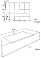
- FIG. 1 shows the first version of a test circuit.
- the capacitor C is charged by a voltage source Q via the resistor R1 and discharged by switching the switch S via the resistor R2 and the test object.
- Resistor R2 only serves to protect source Q and to avoid dangerous body currents in the event of contact.
- the second version of a test circuit is shown in FIG. 4.
- the test circuit of FIG. 4 differs from the test circuit of FIG. 1 in that the resistor R2 of the first version is omitted. By eliminating the resistor R2 in the second version, the full electrical energy of the charged capacitor C acts on the test object in the test circuit of the second version (FIG. 4).
- the first version of the test circuit is primarily used for testing MOS circuits, while the second version is increasingly being used for testing bipolar integrated circuits.
- the corresponding test regulations state that the tests must be carried out with both polarities.
- test methods carried out on integrated circuits have shown that the appearance of the damaged components is that which occurs in practice Appearance largely corresponds, so that the test methods described are used more and more for the assessment of integrated circuits.
- Such test methods for evaluating the protective arrangement are also used to develop protective arrangements for integrated circuits.
- FIG. 2 shows the equivalent circuit used for the simulation of the test circuit according to FIG. 1 (version 1).
- the test object was first replaced by an ohmic load resistance R L.
- the load resistance R L was initially set at 1 ohm.
- the switching process of the switch S is simulated by a voltage jump in the generator Q.
- the relevant switching elements of the discharge circuit are represented in FIG. 2 by the switching elements C, L1, R3, C1, L2, R4, C2, R5, C3, R6 and R L.
- the inductance L1 of the equivalent circuit according to FIG. 2 characterizes the connection inductance of the capacitor C.
- the resistor R3 characterizes the contact resistances of the switch S and the capacitor C1 sets the capacitance of the switch S in the switch position K1 and the supply capacitance to resistor R2.
- Resistor R2 is simulated by switching elements L2, R4, R5, C3 and R6.
- the load is simulated by the resistor R L.
- FIG. 3 shows the result of the simulation on the basis of the equivalent circuit according to FIG. 2.
- the voltage generator Q was switched from zero to 2000 V (plus).
- the current shown in Figure 3 is the current that flows through the load resistor.
- FIG. 5 shows the equivalent circuit for the test circuit according to FIG. 4.
- Inductance L3 characterizes the self-inductance of the discharge circuit
- resistor R7 characterizes the self-damping of the discharge circuit.
- the load is simulated by R L.
- FIG. 6 shows the result of the simulation with the aid of the equivalent circuit according to FIG. 5, namely for a voltage jump of the generator Q at zero time from zero to 500 V.
- R L also has a value of 1 ohm.
- the simulated time range extends from 0 to 100 nsec.
- the power-time profile of FIG. 7 has also been obtained by simulation, namely by product formation of voltage and current at the resistor R L.
- the diagrams show that the short-term load is significantly higher the higher the load resistance in the range of values shown.
- DE-A-29 51 931 describes a protective arrangement with a resistance region which is arranged as a buried layer on a semiconductor substrate.
- the resistance region forms a first diode with the substrate.
- the second diode is connected to the ground potential.
- the circuit to be protected is connected via the resistance range.
- contacts are provided on the two opposite sides of the resistance area.
- the Diodes are connected in parallel between the circuit input and the ground potential.
- WO-A-86 06 213 describes a protective arrangement, the resistance region consisting of a diffusion region.
- EP-A-43 284 shows a protective arrangement which consists of a resistance region over which the circuit arrangement is connected.
- the resistance area forms diodes with the substrate, through which interference is derived.
- the invention has for its object to provide a protective arrangement for an integrated circuit arrangement, which has an improved protective effect and derives the interference on the largest possible area.
- the protective arrangement has an ohmic resistance in the form of one or more resistance areas, which is designed such that it absorbs the essential part of the energy of the electrical disturbance at the limit load and that it distributes the heat generated by the energy absorption in it over such an area of the protective circuit that it is covered by the thermal energy of the ohmic resistor Surface of the protective arrangement is not thermally overloaded, and that the protective arrangement for limiting the interference voltage has a voltage-limiting element or several voltage-limiting elements.
- the voltage-limiting element or the voltage-limiting elements is (are) preferably designed such that the discharge energy supplied to them (them) does not overload the voltage-limiting element or the voltage-limiting elements.
- the ohmic resistance areas are designed as resistance zones in the semiconductor body of the integrated circuit arrangement. It is advantageous to form the resistance zones from semiconductor zones that have a higher impurity concentration (eg greater than 1019 cm ⁇ 3). This avoids the influence of the uncontrollable intrinsic line, which can lead to an unstable current distribution in the semiconductor.
- a resistor in the semiconductor region is arranged at a distance from the semiconductor surface in accordance with a buried layer.
- Another possibility for forming an insulated resistor with a highly doped semiconductor layer is, for example, by using pyer diffusion, which is introduced into a buried layer zone through an n-epitaxial layer.
- a breakthrough in the field strength can make the resistance zone ineffective or partially ineffective. This can e.g. in that the breakthrough section spans the resistance zone in whole or in part.
- the resistance zone is therefore to be designed in such a way that the breakthrough field strength (2 ... 10 x 10 an V / cm) cannot occur at any point in the resistance zone under the maximum stress load.
- the discharge energy is partially converted into thermal energy in the substrate of the semiconductor body (substrate for protective arrangement and integrated circuit arrangement) by conducting the discharge process over the substrate region serving as a resistor.
- This has the advantage that the remaining parts of the protective arrangement can be dimensioned smaller in terms of the crystal area requirement, since their electrical load is lower.
- Another advantage of using the substrate resistance is that the voltage drop in the substrate area is not a voltage load is effective for the zone between the connection pad and the underlying substrate area if this substrate area is connected to the substrate area of the protective arrangement. If the substrate resistance is used, however, it should be noted that, due to the voltage drop in the relevant substrate resistance, the output potential of the protective arrangement is reduced or increased by the voltage drop across the substrate resistance when the fault occurs, depending on the polarity of the fault.
- the desired (required) substrate resistance of the protective arrangement can be realized by appropriate formation of the separation connection zone.
- a "decoupling" of the substrate area of the protective arrangement from the substrate areas of the rest Integrated circuit has the advantage that, in the event of a fault, a greater protective effect for other integrated circuit parts is achieved, going beyond the directly protected circuit part.
- a "decoupling" of the substrate area of the protective arrangement from the substrate areas of the other circuit parts can be achieved, for example, by providing a zone with relatively low conductivity around the substrate area of the associated connection pad of the integrated circuit, which zone includes the low-resistance substrate area of the protective arrangement and from the separates other low-resistance substrate areas of the integrated circuit.
- the low-resistance substrate regions are generally formed by a p-type separation diffusion, while the relatively low conductivity region is determined by the low-doped p-type region of the substrate material of the semiconductor body.
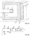
- FIGS. 10 to 14 show the manufacture of a protective arrangement according to the invention, which is intended to protect an integrated circuit arrangement which is located in the same semiconductor body as the protective arrangement, but is not shown in the following figures.
- a semiconductor body 1 also semiconductor body of the integrated circuit arrangement, not shown
- a resistance region 2 is introduced into the semiconductor body 1, the conductivity type of which is opposite to that of the semiconductor body 1 and which therefore has the n-conductivity type in FIG.
- the resistance area 2 is relatively heavily doped and has, for example, an impurity concentration of 1019 cm ⁇ 3.
- an epitaxial layer 3 of the n-type is applied to the semiconductor body 1 (substrate) of the p-type with the resistance region 2 of the n-type, so that the resistance region 2 between the substrate 1 and the epitaxial layer 3 is buried (buried layer).
- a semiconductor zone 4 of the p-conduction type is introduced into the epitaxial layer 3, the regions 4 ′, 4 ′′ and 4 ′′ ′′ of which, with the adjacent resistance region 2, form a zener diode which serves as a voltage-limiting element.
- the p-regions 4 'and 4''additionally perform the function of a separation zone together with the p-region 4''''.
- the p-zone 4 is introduced into the semiconductor body consisting of substrate 1 and epitaxial layer 3 in one operation, for example by diffusion or by ion implantation.
- connection of the resistance region 2 takes place according to FIG. 13 through the connection zones 5 and 6 of the n-type, which are produced after the p-regions, for example also by diffusion or by ion implantation.
- the connection zone 5 of FIG. 13 serves to supply current for the resistance area 2 and is located in the middle of the resistance area 2.
- FIG. 14 shows the finished protective arrangement with an insulating layer 7 on the surface of the epitaxial layer 3 and with an interconnect 8, which leads to the connection zone 5, with an interconnect 9, which covers the p-regions 4 ', 4' 'and 4' ' 'Connects with each other and with an interconnect 10, which establishes an electrical connection between the connection zone 6 and the subsequent integrated circuit arrangement, not shown, in the same semiconductor body.
- FIG. 15 shows the top view of the protective arrangement of FIG. 14.
- FIG. 15 shows an interconnect 9 'which represents the reference point of the subsequent integrated circuit (not shown) to be protected with the reference point (p-regions 4, 4', 4 '', 4 '' ') of the voltage-limiting zener diode of the arrangement according to the invention connects according to Figure 13.
- FIG. 16 shows the equivalent circuit diagram of the protective arrangement of FIGS. 14 and 15.
- the resistance area 2 is divided into the resistance areas 2 ′, 2 ′′ and 2 ′′ ′′, because in the embodiment of the invention according to FIGS. 14 and 15 a large-area diode becomes effective between the resistance region 2 and the substrate 1, which is formed by the pn junction between the resistance region 2 and the substrate 1.
- this diode is represented in simplified form by diodes 11 and 12.
- the Zener diode is designated by the reference number 13.
- the resistor 14 shown in broken lines represents the substrate resistance.
- the connection points of the circuit are designated by the reference numerals 15 'and 16'.
- the operation of the protective arrangement can be explained with the aid of the equivalent circuit according to FIG. 16. If one of the disturbances described occurs at the connection terminals 15 'and 16', the current through the resistors 2 ', 2'',2''' becomes the Zener diode 13 if the interference voltage between the terminals 15 'and 16' is positive as a voltage-limiting element, and the substrate resistor 14 flow. The diodes 11 and 12 are then blocked. If the interference voltage between 15 'and 16' has a negative polarity, the diodes 11 and 12 become conductive, that is to say that the current caused by the interference via the resistance regions 2 ', 2''and2''' to the substrate via the then in the direction of flow effective diodes 11, 12 and 13 flows.
- the resistance areas 2 ', 2'',2''' and 14 are dimensioned and designed such that they absorb the main part of the energy and generate the generated peak load up to which the protective arrangement has to perform its function Emits heat to a larger crystal volume.
- the connection point from the anode of the Zener diode 13 and the substrate region of the Zener diode 13 is selected as the reference point for the subsequent circuit.
- FIG. 17 in order to produce this protective arrangement in a semiconductor body which consists of a substrate 1 of the p-type conduction, a buried layer 2 (resistance region) of the n-conduction type and an epitaxial layer 3 of the n-conduction type, the p-zones 15 , 16 and 17 of the n-conductivity type, to be precise until they come into contact with the substrate 1.
- the p-zones 15, 16 and 17 are produced, for example, by diffusion or by ion implantation.
- the p-zone 15 serves as a separation zone, while the p-zones 16 and 17 are semiconductor zones of Zener diodes.
- connection zones 18, 19 and 20 for the resistance region 2 are produced according to FIG.
- the connection zones 18, 19 and 20 have the n-line type.
- the n-zones 21 and 22 are then produced, the depth of which is less than the depth of the semiconductor zones previously produced in the epitaxial layer 3.
- the semiconductor zone 21 extends from the semiconductor zone 19 to the semiconductor zone 16 and covers these two semiconductor zones.
- the semiconductor zone 22 extends from the semiconductor zone 17 to the semiconductor zone 20 and covers these two semiconductor zones.
- Figure 19 has two Zener diodes, one of which one is formed by the semiconductor zone 21 and the semiconductor zone 16, while the other zener diode is formed by the semiconductor zones 22 and 17.
- the overlap of the semiconductor zone 16 (p+ zone) by the semiconductor zone 21 (n+ zone) and the semiconductor zone 17 by the semiconductor zone 22 has the effect that the barrier layers of these zones do not touch the surface of the semiconductor body 5 at any point, as a result of which the pn- Transition is protected from surface influences.
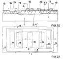
- FIGS. 20 and 21 The finished protective arrangement is shown in FIGS. 20 and 21, specifically FIG. 20 in a sectional view and FIG. 21 in a top view.
- FIGS. 19, 20 and 21 show a protective arrangement in which two Zener diodes act in parallel with one another
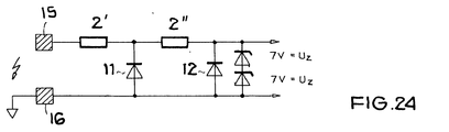
- FIGS. 22 and 23 show a protective arrangement in which two Zener diodes are connected in series and these series connections are effective in parallel with one another.
- the semiconductor body of this protective arrangement again consists of a substrate 1 of the p-type conduction and an epitaxial layer 3 of the n-conduction type.
- three resistance areas 2 ', 2''and2''' in the form of buried layers are provided.
- a separation zone 23 of the p-type conduction which consists of the regions 23a, 23b, 23c, 23e and 23f, is introduced into the epitaxial layer 3.
- the separation region 23a forms a zener diode with the resistance region 2 '
- the separation region 23b forms a zener diode with the resistance region 2'
- the separation region 23c forms with the resistance region 2 ′′ ′′ forms a zener diode
- also the separation region 23d forms a zener diode with the resistance region 2 ′′ ′′.
- the connection zone 27 of the n-line type forms a connection for the resistance region 2 '
- the connection zones 28 and 29 form connections for the resistance region 2 "and the connection zone 30 of the n-line type forms a connection for the resistance region 2"'.
- FIG. 23 shows the finished protective arrangement with the insulating layer 31 on the epitaxial layer 3 and with the electrodes 32, 33, 34 and 35.
- FIG. 24 shows the associated equivalent circuit diagram.
- a protective arrangement according to FIGS. 22, 23 and 24 has the advantage over the protective arrangement according to FIGS. 14, 20 and 21 that the operating voltage for the subsequent circuit to be protected is correspondingly greater due to the series-connected Zener diodes as voltage-limiting element (s) can be chosen.
- a field effect transistor in the protective arrangement has the task of limiting the current that occurs at the output of the protective arrangement in the event of a fault, as a result of which the protective function is expanded. This is done by constricting the channel region of the integrated field effect transistor when a higher (positive) interference voltage occurs at the source electrode.
- the use of a field effect transistor at the output of a protective arrangement according to the invention is suitable for executing protective arrangements which have already been described.
- the resistance of the protective arrangement which must absorb the main part of the energy at the limit load and which is characterized, for example, by the sum of the partial resistances 2 ', 2''and2''' in FIG. 16, should preferably be dimensioned such that the sum of the Voltage drop across this resistor and the value the Zener voltage in the case of the limit load (maximum expected "interference current") does not reach the value of the breakdown voltage for the distance between the connection pad 15 and the area below it, for example oxide layer including n-box.
- Zener diodes with a lower Zener voltage absorb a smaller proportion of the peak energy than those with a higher Zener voltage. If the use of the resistor is provided in the substrate area, as shown in the equivalent circuit according to FIG. 16 with the reference number 14, the energy to be converted into heat which occurs in the other areas is correspondingly reduced in the event of a fault. The smaller the proportion of the energy to be converted into heat in the voltage-limiting element (Zener diode), the smaller the area of this element can be made. This means that if a Zener diode is used as the voltage-limiting element, the area, and also the junction capacitance, which, apart from the doping conditions, depends on the junction area, are reduced. This is important if this junction capacitance has a negative influence on the function of the integrated circuit and if the junction area is reduced, this negative influence can be avoided or reduced.
- FIG. 25 shows a development of the invention in which, in addition to a first protective arrangement 48, a second protective arrangement 49 is provided.
- the protective arrangements 48 and 49 in the arrangement according to FIG. 27 are, for example, designs as described with reference to FIGS. 10, 11, 12, 13, 14, 15 and 16.
- the input 5 of the first protective arrangement 48 is connected via the interconnect 8 to the connection pad 15 'of the integrated circuit.
- the output connection 6 of the first protective arrangement 48 is via the interconnect 10 to the input 5 'of the second protective arrangement 49, and its output 6' connected via the interconnect 10 'to the circuit arrangement (not shown) to be protected.
- the interconnect 51 connects the substrate region 50 of the first protective arrangement 48 to the resistance zone 52 of the p-type conduction, while the contact connection zone 53 'is connected to the reference point 16' (ground) of the integrated circuit.
- the substrate area 54 of the second protective arrangement 49 is connected via the interconnect 55 to the reference point 16 ′ of the integrated circuit and at the same time to the reference point of the circuit arrangement (not shown) to be protected.
- the n-zone 56 which is assigned to the connection pad 15 ', is also included in the substrate region.
- the substrate region 50, in which the first protective arrangement 48 is embedded is “decoupled” from the substrate region 58, in which the second protective arrangement 49 is embedded, by an n-zone 59.
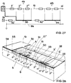
- FIG. 26 shows the sectional illustration of the individual semiconductor zones, based on the section A-A 'of the arrangement according to FIG. 25, and FIG. 28 shows a perspective illustration.
- FIG. 27 shows the equivalent circuit of the arrangement according to FIG. 25 with the elements of the first protection arrangement 48 and the second protection arrangement 49.
- the mode of operation of the protective arrangements has already been described.
- the equivalent circuit according to FIG. 27 should essentially show the “decoupling” of the substrate areas of the two protective arrangements 48 and 49.
- the substrate region 50 is connected to the reference point 16 ′ of the integrated circuit through the resistors 52 ′ and 52 ′′, with an arrangement of the semiconductor zones according to FIG. 25, the resistance 52 ′ is generally smaller than the resistance 52 ′′.
- the substrate region 54 of the second protective arrangement 49 can be assigned to the reference point 16 ′ via the line 55, as a result of which the effective resistance between the substrate zone 50 and the reference point 16 ′ can be dimensioned separately.
- the effective resistance between the substrate zone 50 and the reference point 16 ′ can be determined by designing the resistance zone 52 in FIG. 25.
- the advantage of the arrangement according to FIG. 25 is that a greater protective effect is achieved both for the circuit arrangement to be protected, which is connected downstream of the second protective arrangement (49), and for the other parts of the integrated circuit, because of the "decoupling" of the substrate areas becomes.
- a further advantage of the arrangement according to FIG. 25 is the possibility, by appropriate dimensioning of the substrate resistance (52 ', 52' '), to select the proportion of the discharge energy (disturbance) absorbed by this substrate resistance so large that the protective arrangement 48 and 49 with regard to the need for crystal surfaces can be chosen correspondingly smaller.
- the substrate of the integrated circuit arrangement has the p-line type, but the invention naturally also applies to integrated circuits with a substrate of the n-line type and a correspondingly adapted line type of the other semiconductor zones.
- the resistor provided according to the invention which is provided to protect against high-energy electrical interference, is preferably electrically connected according to FIG. 16 to that connection (pin 15 ', 16') of the integrated circuit arrangement which is affected by the undesired electrical interference.
Description
Die Erfindung betrifft eine Schaltungsanordnung mit einer zumindest teilweise mitintegrierten Schutzanordnung, die die integrierte Schaltungsanordnung vor energiereichen elektrischen Störungen schützt, die auf sie einwirken.The invention relates to a circuit arrangement with an at least partially integrated protective arrangement which protects the integrated circuit arrangement from high-energy electrical disturbances which act on it.
Energiereiche elektrische Störungen sind z.B. Störungen, die durch elektrostatische Entladungen entstehen und die bei der Handhabung von integrierten Schaltungen auf deren Anschlüsse einwirken können und dabei nichtreversible Veränderungen in der integrierten Schaltung bis zu deren Zerstörung verursachen können. Solche elektrostatischen Entladungen treten in vielfältigen Arten und Stärken auf und sind deshalb im einzelnen schwer zu beschreiben. Um jedoch die Empfindlichkeit von integrierten Schaltungen gegenüber solchen Störungen mit einer endlichen Wahrscheinlichkeit erfassen zu können, werden zunehmend - wie bei elektronischen Bauelementen generell - auch integrierte Schaltungen Streßtests unterzogen, bei denen die elektrostatischen Entladungsvorgänge mittels bestimmter Testanordnungen nachgebildet werden. Bei diesen Tests werden nach einem vorgeschriebenen Schema die Anschlüsse der integrierten Schaltung einer bestimmten Impulsbelastung unterzogen.Energy-rich electrical disturbances are, for example, disturbances which arise from electrostatic discharges and which can affect their connections when handling integrated circuits and can thereby cause irreversible changes in the integrated circuit until they are destroyed. Such electrostatic discharges occur in various types and strengths and are therefore difficult to describe in detail. However, in order to be able to detect the sensitivity of integrated circuits to such disturbances with a finite probability, stress is also increasingly being applied to integrated circuits, as is generally the case with electronic components, in which the electrostatic discharge processes are simulated using specific test arrangements. In these tests, the connections of the integrated circuit are subjected to a specific pulse load according to a prescribed scheme.
Im Prinzip wird bei Streßtests ein Kondensator vorgegebener Kapazität auf eine vorgegebene Spannung aufgeladen und unter bestimmten Bedingungen über das zu testende Bauelement entladen. In der Praxis werden zwei Versionen von Testschaltungen bevorzugt, die im folgenden näher beschrieben werden. Die erste Version einer Testschaltung zeigt die Figur 1. Bei der Testschaltung der Figur 1 wird der Kondensator C von einer Spannungsquelle Q über den Widerstand R1 geladen und durch Umschalten des Schalters S über den Widerstand R2 und das Testobjekt entladen. Der Widerstand R2 dient hierbei nur zum Schutz der Quelle Q und zur Vermeidung gefährlicher Körperströme im Berührungsfalle.In principle, a capacitor with a given capacitance is charged to a given voltage during stress tests and discharged under certain conditions via the component to be tested. In practice, two versions of test circuits are preferred, which are described in more detail below. FIG. 1 shows the first version of a test circuit. In the test circuit of FIG. 1, the capacitor C is charged by a voltage source Q via the resistor R1 and discharged by switching the switch S via the resistor R2 and the test object. Resistor R2 only serves to protect source Q and to avoid dangerous body currents in the event of contact.
Die zweite Version einer Testschaltung zeigt die Figur 4. Die Testschaltung der Figur 4 unterscheidet sich von der Testschaltung der Figur 1 dadurch, daß bei ihr der Widerstand R2 der ersten Version entfällt. Durch den Wegfall des Widerstandes R2 bei der zweiten Version wirkt bei der Testschaltung der zweiten Version (Figur 4) die volle elektrische Energie des geladenen Kondensators C auf das Testobjekt ein. Die erste Version der Testschaltung wird vornehmlich für den Test von MOS-Schaltungen eingesetzt, während in zunehmenden Maße die zweite Version zum Testen von bipolaren integrierten Schaltungen eingesetzt wird. Die entsprechenden Testvorschriften besagen, daß die Tests mit beiden Polaritäten durchzuführen sind.The second version of a test circuit is shown in FIG. 4. The test circuit of FIG. 4 differs from the test circuit of FIG. 1 in that the resistor R2 of the first version is omitted. By eliminating the resistor R2 in the second version, the full electrical energy of the charged capacitor C acts on the test object in the test circuit of the second version (FIG. 4). The first version of the test circuit is primarily used for testing MOS circuits, while the second version is increasingly being used for testing bipolar integrated circuits. The corresponding test regulations state that the tests must be carried out with both polarities.
Die an integrierten Schaltungen durchgeführten Streßtests haben gezeigt, daß das Erscheinungsbild der geschädigten Bauelemente dem in der Praxis auftretenden Erscheinungsbild weitgehend entspricht, so daß die beschriebenen Testmethoden mehr und mehr mit zur Beurteilung von integrierten Schaltungen herangezogen werden. Auch werden zur Entwicklung von Schutzanordnungen für integrierte Schaltungen solche Testverfahren zur Bewertung der Schutzanordnung verwendet.The stress tests carried out on integrated circuits have shown that the appearance of the damaged components is that which occurs in practice Appearance largely corresponds, so that the test methods described are used more and more for the assessment of integrated circuits. Such test methods for evaluating the protective arrangement are also used to develop protective arrangements for integrated circuits.
Um einen Überlick über die Vorgänge zu erhalten, die sich bei den Testversuchen mittels der bekannten Testschaltungen (Version 1 oder Version 2) abspielen, wurden die ablaufenden Entladungsvorgänge durch Simulation erfaßt, da diese wegen des nichtperiodischen und schnellen Ablaufs der Vorgänge meßtechnisch praktisch nicht zu erfassen sind. Hierzu mußte zunächst die Testschaltung in eine für die Simulation geeignete Ersatzschaltung umgewandelt werden. Die Figur 2 zeigt die zur Simulation eingesetzte Ersatzschaltung der Testschaltung nach Figur 1 (Version 1). Bei der Simulation wurde das Testobjekt zunächst durch einen ohmschen Lastwiderstand RL ersetzt. Der Lastwiderstand RL wurde zunächst mit 1 Ohm angesetzt. In der Ersatzschaltung nach Figur 2 wird der Umschaltvorgang des Schalters S durch einen Spannungssprung des Generators Q simuliert. Die maßgebenden Schaltelemente des Entladungskreises sind nach Figur 2 durch die Schaltelemente C, L1, R3, C1, L2, R4, C2, R5, C3, R6 und RL dargestellt.In order to obtain an overview of the processes that take place in the test attempts using the known test circuits (
Die Induktivität L1 der Ersatzschaltung nach Figur 2 charakterisiert die Anschlußinduktivität des Kondensators C. Der Widerstand R3 charakterisiert die Übergangswiderstände des Schalters S und der Kondensator C1 stellt die Kapazität des Schalters S in der Schalterstellung K1 sowie die Zuleitungskapazitäten zum Widerstand R2 dar. Der Widerstand R2 wird durch die Schaltelemente L2, R4, R5, C3 und R6 nachgebildet. Die Lastnachbildung erfolgt durch den Widerstand RL.The inductance L1 of the equivalent circuit according to FIG. 2 characterizes the connection inductance of the capacitor C. The resistor R3 characterizes the contact resistances of the switch S and the capacitor C1 sets the capacitance of the switch S in the switch position K1 and the supply capacitance to resistor R2. Resistor R2 is simulated by switching elements L2, R4, R5, C3 and R6. The load is simulated by the resistor R L.
Die Figur 3 zeigt das Ergebnis der Simulation bei Zugrundelegung der Ersatzschaltung nach Figur 2. Bei der Simulation wurde der Spannungsgenerator Q von Null auf 2000 V (plus) geschaltet. Die Figur 3 zeigt den Stromverlauf in Abhängigkeit von der Zeit bei Verwendung eines ohmschen Widerstandes RL = 1 Ohm als Lastnachbildung. Der in der Figur 3 dargestellte Strom ist der Strom, der durch den Lastwiderstand fließt.FIG. 3 shows the result of the simulation on the basis of the equivalent circuit according to FIG. 2. In the simulation, the voltage generator Q was switched from zero to 2000 V (plus). FIG. 3 shows the current curve as a function of time when using an ohmic resistor R L = 1 ohm as a load simulation. The current shown in Figure 3 is the current that flows through the load resistor.
Die Figur 5 zeigt die Ersatzschaltung für die Testschaltung nach der Figur 4. Die Induktivität L3 charakterisiert die Eigeninduktivität des Entladekreises, während der Widerstand R7 die Eigendämpfung des Entladekreises charakterisiert. Die Lastnachbildung erfolgt durch RL.FIG. 5 shows the equivalent circuit for the test circuit according to FIG. 4. Inductance L3 characterizes the self-inductance of the discharge circuit, while resistor R7 characterizes the self-damping of the discharge circuit. The load is simulated by R L.
Die Figur 6 zeigt das Ergebnis der Simulation mit Hilfe der Ersatzschaltung nach Figur 5 , und zwar für einen Spannungssprung des Generators Q im Zeitpunkt Null von Null auf 500 V. RL hat dabei ebenfalls einen Wert von 1 Ohm. Wie in der Figur 3 erstreckt sich der simulierte Zeitbereich (Abszisse) von 0 bis 100 nsec.FIG. 6 shows the result of the simulation with the aid of the equivalent circuit according to FIG. 5, namely for a voltage jump of the generator Q at zero time from zero to 500 V. R L also has a value of 1 ohm. As in FIG. 3, the simulated time range (abscissa) extends from 0 to 100 nsec.
Vergleicht man die Figuren 3 und 6 miteinander, so sieht man, daß bei Anwendung der zweiten Testschaltung (Figur 4) wesentlich höhere Ströme auftreten als bei Anwendung der ersten Testschaltung (Figur 1). Dieses Ergebnis gilt für beide Polaritäten der Generatorspannung. Dabei ist noch zu berücksichtigen, daß die Spannung des Generators Q, die bei der zweiten Testmethode angewendet wurde, wesentlich niedriger ist als die Spannung, die bei der ersten Testmethode angewendet wurde, nämlich 500 V im Vergleich zu 2000 V bei der ersten Testmethode.Comparing FIGS. 3 and 6 with one another, it can be seen that when using the second test circuit (FIG. 4) significantly higher currents occur than when using the first test circuit (FIG. 1). This result applies to both polarities of the generator voltage. It should also be considered that the voltage of the generator Q used in the second test method is significantly lower than the voltage used in the first test method, namely 500 V compared to 2000 V in the first test method.
Aus diesem Vergleich ergibt sich, daß die zweite Testmethode für den zu testenden integrierten Schaltkreis wesentlich kritischer ist (erscheint) als die erste Testmethode.This comparison shows that the second test method for the integrated circuit to be tested is (appears) much more critical than the first test method.
Neben dem Strom-Zeitverlauf interessiert auch der Leistungs-Zeitverlauf. Die Figur 7 zeigt den Leistungs-Zeitverlauf am Lastwiderstand RL, wenn RL = 1 Ohm ist. Der Leistungs-Zeitverlauf der Figur 7 ist ebenfalls durch Simulation gewonnen worden, und zwar durch Produktbildung von Spannung und Strom am Widerstand RL. Der Strom-Zeitverlauf wurde mittels der Ersatzschaltung nach Figur 4 ermittelt. Dies gilt auch für die Figuren 8 und 9, von denen die Figur 8 den Strom-Zeitverlauf für einen Lastwiderstand RL = 11 Ohm und Figur 9 den Leistungs-Zeitverlauf ebenfalls für einen Lastwiderstand RL = 11 Ohm zeigt. Danach bedingt ein höherer Wert für RL das Auftreten einer wesentlich höheren Spitzenleistung bei gleichzeitig schnellerem Abklingen. Die Darstellungen zeigen, daß die Kurzzeitbelastung wesentlich höher ist, je höher der Lastwiderstand in dem dargestellten Wertebereich ist.In addition to the current-time curve, the power-time curve is also of interest. FIG. 7 shows the power-time profile at the load resistor R L when R L = 1 ohm. The power-time profile of FIG. 7 has also been obtained by simulation, namely by product formation of voltage and current at the resistor R L. The current-time profile was determined using the equivalent circuit shown in FIG. 4. This also applies to FIGS. 8 and 9, of which FIG. 8 shows the current-time profile for a load resistance R L = 11 ohms and FIG. 9 also shows the power-time profile for a load resistance R L = 11 ohms. Thereafter, a higher value for R L causes a significantly higher peak power to occur with a faster decay. The diagrams show that the short-term load is significantly higher the higher the load resistance in the range of values shown.
Untersuchungen haben gezeigt, daß integrierte Schaltungen, die den beschriebenen Tests unterzogen werden, häufig im Bereich der belasteten Schaltungsteile lokale "Schmelzkanäle" aufweisen, die auf starke lokale Erhitzung zurückzuführen sind. Solche Erscheinungen finden sich vorwiegend in den Halbleiterzonen mit niedriger Dotierung. Es ist daher wahrscheinlich, daß die "Schmelzkanäle" durch temperaturinjizierte Eigenleitung des Halbleitermaterials entstehen, die ab bestimmten Temperaturen die Störstellenleitung übersteigt. Da die Eigenleitung (Intrinsicdichte) exponentiell mit der Temperatur ansteigt, konzentriert sich in einem solchen "angefachten" Halbleiterbereich der Strom lawinenartig und erhitzt so lokal das Halbleitermaterial. Dieser Vorgang ist im allgemeinen nicht kontrollierbar. Dies wird verständlich, wenn, wie die Theorie über die Temperaturabhängigkeit der Eigenleitfähigkeit (Intrinsicdichte) für Silizium aussagt, in einer Siliziumzone mit einer Störstellenkonzentration von z.B. 10¹⁵ cm⁻³ bereits bei einer Temperatur von ca. 280 °C die Eigenleitung für den elektrischen Widerstand bestimmend ist, d.h. ab einer solchen Kristalltemperatur die Leitfähigkeit exponentiell ansteigt. Vergleichsweise ist bei einer Störstellenkonzentration von 10¹⁹ cm⁻³ dies erst ab ca. 1400 °C der Fall, also bei Temperaturen nahe dem Schmelzpunkt des Siliziums.Investigations have shown that integrated circuits which are subjected to the tests described often have local “melting channels” in the area of the loaded circuit parts, which are subject to strong local heating are due. Such phenomena are mainly found in the semiconductor zones with low doping. It is therefore likely that the "melting channels" arise from the temperature-injected intrinsic conduction of the semiconductor material, which exceeds the impurity conduction from certain temperatures. Since the intrinsic density (intrinsic density) increases exponentially with the temperature, the current in such a "fanned" semiconductor area is concentrated like an avalanche and thus heats up the semiconductor material locally. This process is generally not controllable. This is understandable if, as the theory says about the temperature dependence of the intrinsic conductivity (intrinsic density) for silicon, in a silicon zone with an impurity concentration of e.g. 10¹⁵ cm⁻³ already at a temperature of approx. 280 ° C the intrinsic conductor determines the electrical resistance is, ie the conductivity increases exponentially from such a crystal temperature. By comparison, with an impurity concentration of 10¹⁹ cm⁻³ this is only the case from approx. 1400 ° C, ie at temperatures close to the melting point of the silicon.
Die DE-A-29 51 931 beschreibt eine Schutzanordnung mit einem Widerstandsbereich, der als vergrabene Schicht auf einem Halbleiterstubstrat angeordnet ist. Der Widerstandsbereich bildet mit dem Substrat eine erste Diode. Auf dem Widerstandsbereich befinden sich epitaktische Schichten, die eine zweite Diodenstruktur bilden. Die zweite Diode wird ebenso wie die erste Diode mit dem Massepotential verbunden. Der Anschluß der zu schützenden Schaltung erfolgt über den Widerstandsbereich. An den beiden gegenüberliegenden Seiten des Widerstandsbereichs sind dazu Kontakte vorgesehen. Die Dioden liegen parallel zwischen dem Schaltungseingang und dem Massepotential.DE-A-29 51 931 describes a protective arrangement with a resistance region which is arranged as a buried layer on a semiconductor substrate. The resistance region forms a first diode with the substrate. There are epitaxial layers on the resistance area, which form a second diode structure. Like the first diode, the second diode is connected to the ground potential. The circuit to be protected is connected via the resistance range. For this purpose, contacts are provided on the two opposite sides of the resistance area. The Diodes are connected in parallel between the circuit input and the ground potential.
Die WO-A-86 06 213 beschreibt eine Schutzanordnung, wobei der Widerstandsbereich aus einem Diffusionsgebiet besteht.WO-A-86 06 213 describes a protective arrangement, the resistance region consisting of a diffusion region.
Die EP-A-43 284 zeigt eine Schutzanordnung, die aus einem Widerstandsbereich besteht, über den der Anschluß der Schaltungsanordnung erfolgt. Der Widerstandsbereich bildet mit dem Substrat Dioden, über die Störungen abgeleitet werden.EP-A-43 284 shows a protective arrangement which consists of a resistance region over which the circuit arrangement is connected. The resistance area forms diodes with the substrate, through which interference is derived.
Der Erfindung liegt die Aufgabe zugrunde, eine Schutzanordnung für eine integrierte Schaltungsanordnung anzugeben, die eine verbesserte Schutzwirkung aufweist und die Störungen auf eine möglichst große Fläche ableitet.The invention has for its object to provide a protective arrangement for an integrated circuit arrangement, which has an improved protective effect and derives the interference on the largest possible area.
Diese Aufgabe wird durch eine Anordnung mit den kennzeichnenden Merkmalen der Ansprüche 1 oder 2 gelöst. Die vorteilhafte Ausgestaltung der Erfindung erfolgt gemäß den Merkmalen der abhängigen Ansprüche.This object is achieved by an arrangement with the characterizing features of
Die Schutzanordnung weist einen ohmschen Widerstand in Gestalt von einem oder mehreren Widerstandsbereichen auf, der derart ausgebildet ist, daß er bei Grenzbelastung den wesentlichen Teil der Energie der elektrischen Störung aufnimmt und daß er die Wärme, die durch die Energieaufnahme in ihm erzeugt wird, auf eine solche Fläche der Schutzschaltung verteilt, daß die von der Wärmeenergie des ohmschen Widerstandes erfaßte Fläche der Schutzanordnung thermisch nicht überbelastet wird, und daß die Schutzanordnung zur Begrenzung der Störspannung ein spannungsbegrenzendes Element oder mehrere spannungsbegrenzende Elemente aufweist.The protective arrangement has an ohmic resistance in the form of one or more resistance areas, which is designed such that it absorbs the essential part of the energy of the electrical disturbance at the limit load and that it distributes the heat generated by the energy absorption in it over such an area of the protective circuit that it is covered by the thermal energy of the ohmic resistor Surface of the protective arrangement is not thermally overloaded, and that the protective arrangement for limiting the interference voltage has a voltage-limiting element or several voltage-limiting elements.
Das spannungsbegrenzende Element bzw. die spannungsbegrenzenden Elemente ist (sind) vorzugsweise so ausgebildet, daß die ihm (ihnen) zugeführte Entladungsenergie das spannungsbegrenzende Element bzw. die spannungsbegrenzenden Elemente nicht überlastet.The voltage-limiting element or the voltage-limiting elements is (are) preferably designed such that the discharge energy supplied to them (them) does not overload the voltage-limiting element or the voltage-limiting elements.
Die ohmschen Widerstandsbereiche sind als Widerstandszonen im Halbleiterkörper der integrierten Schaltungsanordnung ausgebildet. Es ist vorteilhaft, die Widerstandszonen aus Halbleiterzonen zu bilden, die eine höhere Störstellenkonzentration (z.B. größer 10¹⁹ cm⁻³) aufweisen. Dadurch wird der Einfluß der unkontrollierbaren Eigenleitung, die zu einer instabilen Stromverteilung im Halbleiter führen kann, vermieden. Ein Widerstand im Halbleiterbereich ist im Abstand von der Halbleiteroberfläche entsprechend einer buried layer angeordnet.The ohmic resistance areas are designed as resistance zones in the semiconductor body of the integrated circuit arrangement. It is advantageous to form the resistance zones from semiconductor zones that have a higher impurity concentration (eg greater than 10¹⁹ cm⁻³). This avoids the influence of the uncontrollable intrinsic line, which can lead to an unstable current distribution in the semiconductor. A resistor in the semiconductor region is arranged at a distance from the semiconductor surface in accordance with a buried layer.
Eine weitere Möglichkeit, einen isolierten Widerstand mit hochdotierter Halbleiterschicht zu bilden, besteht beispielsweise durch die Verwendung einer p⁺-Diffusion, die durch eine n-Epitaxialschicht in eine buried layer-Zone eingebracht wird.Another possibility for forming an insulated resistor with a highly doped semiconductor layer is, for example, by using p einer diffusion, which is introduced into a buried layer zone through an n-epitaxial layer.
Ein anderer Aspekt für die erfindungsgemäße Ausbildung der Widerstandszone ist das Vermeiden eines Feldstärkedurchbruchs in der Widerstandszone. Durch einen Feldstärkedurchbruch kann nämlich die Widerstandszone unwirksam oder teilweise unwirksam werden. Dies kann z.B. dadurch entstehen, daß die Durchbruchstrecke die Widerstandszone ganz oder teilweise überbrückt. Die Widerstandszone ist daher so anzulegen, daß bei der maximal auftretenden Streßbelastung an keiner Stelle der Widerstandszone die Durchbruchfeldstärke (2...10 x 10⁵ V/cm) auftreten kann.Another aspect for the formation of the resistance zone according to the invention is the avoidance of a field strength breakthrough in the resistance zone. A breakthrough in the field strength can make the resistance zone ineffective or partially ineffective. This can e.g. in that the breakthrough section spans the resistance zone in whole or in part. The resistance zone is therefore to be designed in such a way that the breakthrough field strength (2 ... 10 x 10 an V / cm) cannot occur at any point in the resistance zone under the maximum stress load.
Gemäß einer Weiterbildung der Erfindung ist vorgesehen, daß die Entladungsenergie teilweise im Substrat des Halbleiterkörpers (Substrat für Schutzanordnung und integrierte Schaltungsanordnung) in Wärmeenergie umgesetzt wird, indem der Entladungsvorgang über den als Widerstand dienenden Substratbereich geleitet wird. Dies hat den Vorteil, daß die übrigen Teile der Schutzanordnung hinsichtlich des Kristallflächenbedarfs kleiner bemessen werden können, da deren elektrische Belastung geringer ist. Ein weiterer Vorteil der Nutzung des Substratwiderstandes besteht darin, daß der Spannungsabfall im Substratbereich nicht als Spannungsbelastung für die Zone zwischen dem Anschluß-Pad und dem darunter liegenden Substratbereich wirksam ist, wenn dieser Substratbereich mit dem Substratbereich der Schutzanordnung verbunden ist. Im Falle der Nutzung des Substratwiderstandes ist jedoch zu beachten, daß, durch den Spannungsabfall im maßgebenden Substratwiderstand bedingt, das Ausgangspotential der Schutzanordnung bei Auftreten der Störung um die am Substratwiderstand abfallende Spannung, je nach Polarität der Störung, vermindert oder angehoben wird.According to a development of the invention, it is provided that the discharge energy is partially converted into thermal energy in the substrate of the semiconductor body (substrate for protective arrangement and integrated circuit arrangement) by conducting the discharge process over the substrate region serving as a resistor. This has the advantage that the remaining parts of the protective arrangement can be dimensioned smaller in terms of the crystal area requirement, since their electrical load is lower. Another advantage of using the substrate resistance is that the voltage drop in the substrate area is not a voltage load is effective for the zone between the connection pad and the underlying substrate area if this substrate area is connected to the substrate area of the protective arrangement. If the substrate resistance is used, however, it should be noted that, due to the voltage drop in the relevant substrate resistance, the output potential of the protective arrangement is reduced or increased by the voltage drop across the substrate resistance when the fault occurs, depending on the polarity of the fault.
Um negative Einflüsse dieses Spannungsabfalls auf die zu schützende Schaltung zu vermeiden, empfiehlt es sich, den massebezogenen Bezugspunkt der zu schützenden Schaltung unmittelbar dem Substratbereich zuzuordnen, mit dem das spannungsbegrenzende Element der Schutzanordnung verbunden ist. Damit wird sichergestellt, daß der zu schützenden Schaltung im Störfalle nur Spitzenspannungen zugeführt werden, die der Größe der an den spannungsbegrenzenden Elementen der Schutzanordnung auftretenden Spannungen entsprechen.In order to avoid negative influences of this voltage drop on the circuit to be protected, it is advisable to assign the ground-related reference point of the circuit to be protected directly to the substrate area to which the voltage-limiting element of the protective arrangement is connected. This ensures that, in the event of a fault, the circuit to be protected is supplied with only peak voltages which correspond to the magnitude of the voltages occurring at the voltage-limiting elements of the protective arrangement.
Ferner ist es vorteilhaft, den Substratbereich der Schutzanordnung von den übrigen Substratbereichen der integrierten Schaltung zu "entkoppeln" und den Substratbereich der Schutzanordnung mit dem Bezugspunkt (Masse) der integrierten Schaltung über eine separate Leitbahn zu verbinden, wobei der gewünschte (erforderliche) Substratwiderstand der Schutzanordnung durch entsprechende Ausbildung der Separationsanschlußzone realisiert werden kann. Eine "Entkopplung" des Substratbereiches der Schutzanordnung von den Substratbereichen der übrigen integrierten Schaltung hat den Vorteil, daß dadurch im Störungsfall, über den unmittelbar geschützten Schaltungsteil hinausgehend, eine größere Schutzwirkung für andere integrierte Schaltungsteile erreicht wird.Furthermore, it is advantageous to "decouple" the substrate area of the protective arrangement from the other substrate areas of the integrated circuit and to connect the substrate area of the protective arrangement to the reference point (ground) of the integrated circuit via a separate interconnect, the desired (required) substrate resistance of the protective arrangement can be realized by appropriate formation of the separation connection zone. A "decoupling" of the substrate area of the protective arrangement from the substrate areas of the rest Integrated circuit has the advantage that, in the event of a fault, a greater protective effect for other integrated circuit parts is achieved, going beyond the directly protected circuit part.
Eine "Entkopplung" des Substratbereichs der Schutzanordnung von den Substratbereichen der anderen Schaltungsteile kann beispielsweise dadurch realisiert werden, daß um den Substratbereich des zugeordneten AnschlußPads der integrierten Schaltung, eine Zone mit verhältnismäßig geringer Leitfähigkeit vorgesehen ist, die den niederohmigen Substratbereich der Schutzanordnung einschließt und von den anderen niederohmigen Substrathereichen der integrierten Schaltung trennt. Die niederohmigen Substratbereiche werden im allgemeinen durch eine Separationsdiffusion vom p-Leitungstyp gebildet, während die Zone mit der verhältnismäßig niederen Leitfähigkeit durch den niederdotierten Bereich vom p-Leitungstyp des Substratmaterials des Halbleiterkörpers bestimmt wird.A "decoupling" of the substrate area of the protective arrangement from the substrate areas of the other circuit parts can be achieved, for example, by providing a zone with relatively low conductivity around the substrate area of the associated connection pad of the integrated circuit, which zone includes the low-resistance substrate area of the protective arrangement and from the separates other low-resistance substrate areas of the integrated circuit. The low-resistance substrate regions are generally formed by a p-type separation diffusion, while the relatively low conductivity region is determined by the low-doped p-type region of the substrate material of the semiconductor body.
Die Erfindung wird im folgenden an Ausführungsbeispielen erläutert.The invention is explained below using exemplary embodiments.
Die Figuren 10 bis 14 zeigen die Herstellung einer Schutzanordnung nach der Erfindung, die eine integrierte Schaltungsanordnung schützen soll, die sich im selben Halbleiterkörper wie die Schutzanordnung befindet, jedoch in den folgenden Figuren nicht dargestellt ist. Gemäß der Figur 10 geht man bei der Herstellung der Schutzanordnung von einem Halbleiterkörper 1 (auch Halbleiterkörper der nicht dargestellten integrierten Schaltungsanordnung) aus, der im Ausführungsbeispiel den p-Leitungstyp aufweist. In den Halbleiterkörper 1 wird gemäß der Figur 10 ein Widerstandsbereich 2 eingebracht, dessen Leitungstyp dem des Halbleiterkörpers 1 entgegengesetzt ist und der somit in der Figur 10 den n-Leitungstyp aufweist. Der Widerstandsbereich 2 ist relativ stark dotiert und weist beispielsweise eine Störstellenkonzentration von 10¹⁹ cm⁻³ auf.FIGS. 10 to 14 show the manufacture of a protective arrangement according to the invention, which is intended to protect an integrated circuit arrangement which is located in the same semiconductor body as the protective arrangement, but is not shown in the following figures. According to FIG. 10, a semiconductor body 1 (also semiconductor body of the integrated circuit arrangement, not shown) is used to manufacture the protective arrangement. from which has the p-line type in the exemplary embodiment. According to FIG. 10, a
Nach der Figur 11 wird auf den Halbleiterkörper 1 (Substrat) vom p-Leitungstyp mit dem Widerstandsbereich 2 vom n-Leitungstyp eine epitaktische Schicht 3 vom n-Leitungstyp aufgebracht, so daß der Widerstandsbereich 2 zwischen dem Substrat 1 und der epitaktischen Schicht 3 begraben ist (buried layer). Nach der Figur 12 wird in die epitaktische Schicht 3 eine Halbleiterzone 4 vom p-Leitungstyp eingebracht, deren Bereiche 4', 4'' und 4''' mit dem angrenzenden Widerstandsbereich 2 eine Zenerdiode bilden, die als spannungsbegrenzendes Element dient. Die p-Bereiche 4' und 4'' erfüllen zusätzlich noch zusammen mit dem p-Bereich 4'''' die Funktion einer Separationszone. Der p-Bereich 4''' berührt den Widerstandsbereich 2 auf der gesamten Unterseite, während der p-Bereich 4' den Widerstandsbereich nur am Rande berührt. Die p-Bereiche 4', 4'', 4''' und 4'''' werden so tief eingebracht, daß sie den Widerstandsbereich 2 bzw. das Substrat 1 berühren. Die p-Zone 4 wird in einem Arbeitsgang in den aus Substrat 1 und epitaktischer Schicht 3 bestehenden Halbleiterkörper eingebracht, und zwar beispielsweise durch Diffusion oder durch Ionenimplantation.According to FIG. 11, an
Der Anschluß des Widerstandsbereichs 2 erfolgt gemäß der Figur 13 durch die Anschlußzonen 5 und 6 vom n-Leitungstyp, die nach den p-Bereichen hergestellt werden, und zwar beispielsweise ebenfalls durch Diffusion oder durch Ionenimplantation. Die Anschlußzone 5 der Figur 13 dient zur Stromzufuhr für den Widerstandsbereich 2 und liegt in der Mitte des Widerstandsbereichs 2.The connection of the
Die Figur 14 zeigt die fertige Schutzanordnung mit einer Isolierschicht 7 auf der Oberfläche der epitaktischen Schicht 3 sowie mit einer Leitbahn 8, die zur Anschlußzone 5 führt, mit einer Leitbahn 9, die die p-Bereiche 4', 4'' und 4''' miteinander verbindet und mit einer Leitbahn 10, die eine elektrische Verbindung zwischen der Anschlußzone 6 und der nachfolgenden, nicht dargestellten integrierten Schaltungsanordnung im selben Halbleiterkörper herstellt.FIG. 14 shows the finished protective arrangement with an insulating
Die Figur 15 zeigt die Draufsicht auf die Schutzanordnung der Figur 14.FIG. 15 shows the top view of the protective arrangement of FIG. 14.
In der Figur 15 ist eine Leitbahn 9' angegebenen, die den Bezugspunkt der nachfolgenden, nicht dargestellten zu schützenden integrierten Schaltung mit dem Bezugspunkt (p-Bereiche 4, 4', 4'', 4''') der spannungsbegrenzenden Zenerdiode der erfindungsgemäßen Anordnung nach der Figur 13 verbindet.FIG. 15 shows an interconnect 9 'which represents the reference point of the subsequent integrated circuit (not shown) to be protected with the reference point (p-
Die Figur 16 zeigt das Ersatzschaltbild der Schutzanordnung der Figuren 14 und 15. Beim Ersatzschaltbild der Figur 16 ist der Widerstandsbereich 2 in die Widerstandsbereiche 2', 2'' und 2''' aufgeteilt, weil in der Ausführungsform der Erfindung nach Figur 14 und 15 zwischen dem Widerstandsbereich 2 und dem Substrat 1 eine großflächige Diode wirksam wird, die durch den pn-Übergang zwischen dem Widerstandsbereich 2 und dem Substrat 1 gebildet wird. Diese Diode wird in der Ersatzschaltung nach Figur 16 vereinfacht durch die Dioden 11 und 12 dargestellt. Die Zenerdiode ist mit der Bezugsziffer 13 bezeichnet. Der gestrichelt eingezeichnete Widerstand 14 stellt den Substratwiderstand dar. Die Anschlußpunkte der Schaltung sind mit den Bezugsziffern 15' und 16' bezeichnet.FIG. 16 shows the equivalent circuit diagram of the protective arrangement of FIGS. 14 and 15. In the equivalent circuit diagram of FIG. 16, the
Mit Hilfe der Ersatzschaltung nach Figur 16 kann die Funktionsweise der Schutzanordnung erklärt werden. Tritt an den Anschlußklemmen 15' und 16' eine der beschriebenen Störungen auf, so wird bei positiver Polarität der auftretenden Störspannung zwischen Anschluß 15' und 16' der Strom über die Widerstände 2', 2'', 2''', die Zenerdiode 13 als spannungsbegrenzendes Element, und den Substratwiderstand 14 fließen. Die Dioden 11 und 12 sind dann gesperrt. Weist die Störspannung zwischen 15' und 16' eine negative Polarität auf, werden die Dioden 11 und 12 leitend, d.h., daß der durch die Störung verursachte Strom über die Widerstandsbereiche 2', 2'' und 2''' zum Substrat über die dann in Flußrichtung wirksamen Dioden 11, 12 und 13 abfließt. Erfindungsgemäß werden die Widerstandsbereiche 2', 2'', 2''' und 14 so bemessen und ausgeführt, daß sie bei der zu erwartenden Spitzenbelastung, bis zu der die Schutzanordnung ihre Funktion zu erfüllen hat, den Hauptteil der Energie aufnimmt und die dabei erzeugte Wärme auf ein größeres Kristallvolumen abgibt. Um den durch den Stromfluß erzeugten Spannungsabfall an dem Substratwiderstand 14 nicht auf die nachfolgende zu schützende integrierte Schaltung wirksam werden zu lassen, ist vorzugsweise vorgesehen, daß als Bezugspunkt für die nachfolgende Schaltung der Verbindungspunkt von der Anode der Zenerdiode 13 und dem Substratbereich der Zenerdiode 13 gewählt wird.The operation of the protective arrangement can be explained with the aid of the equivalent circuit according to FIG. 16. If one of the disturbances described occurs at the connection terminals 15 'and 16', the current through the resistors 2 ', 2'',2''' becomes the
Im folgenden wird die Herstellung einer anderen Ausführungsform einer Schutzanordnung nach der Erfindung beschrieben. Nach der Figur 17 werden zur Herstellung dieser Schutzanordnung in einem Halbleiterkörper, der aus einem Substrat 1 vom p-Leitungstyp, einer buried layer 2 (Widerstandsbereich) vom n-Leitungstyp und einer epitaktischen Schicht 3 vom n-Leitungstyp besteht, die p-Zonen 15, 16 und 17 vom n-Leitungstyp eingebracht, und zwar bis zur Berührung mit dem Substrat 1. Die p-Zonen 15, 16 und 17 werden beispielsweise durch Diffusion oder durch Ionenimplantation hergestellt. Die p-Zone 15 dient als Separationszone, während die p-Zonen 16 und 17 Halbleiterzonen von Zenerdioden sind.The manufacture of another embodiment of a protective arrangement according to the invention is described below. According to FIG. 17, in order to produce this protective arrangement in a semiconductor body which consists of a
Nach der Herstellung der p-Zonen 15, 16 und 17 werden gemäß der Figur 18 die Anschlußzonen 18, 19 und 20 für den Widerstandsbereich 2 hergestellt. Die Anschlußzonen 18, 19 und 20 haben den n-Leitungstyp. Gemäß der Figur 19 werden anschließend die n-Zonen 21 und 22 hergestellt, deren Tiefe geringer ist als die Tiefe der zuvor in der epitaktischen Schicht 3 hergestellten Halbleiterzonen. Die Halbleiterzone 21 erstreckt sich von der Halbleiterzone 19 zur Halbleiterzone 16 und bedeckt diese beiden Halbleiterzonen. Die Halbleiterzone 22 erstreckt sich von der Halbleiterzone 17 zur Halbleiterzone 20 und überdeckt diese beiden Halbleiterzonen. Die Figur 19 weist zwei Zenerdioden auf, von denen die eine durch die Halbleiterzone 21 und die Halbleiterzone 16 gebildet wird, während die andere Zenerdiode durch die Halbleiterzonen 22 und 17 gebildet wird.After the production of the p-
Die Überlappung der Halbleiterzone 16 (p⁺-Zone) durch die Halbleiterzone 21 (n⁺-Zone) und der Halbleiterzone 17 durch die Halbleiterzone 22 bewirkt, daß die Sperrschichten dieser Zonen an keiner Stelle die Oberfläche des Halbleiterkörpers 5 berühren, wodurch der p-n-Übergang vor Oberflächeneinflüßen geschützt ist.The overlap of the semiconductor zone 16 (p⁺ zone) by the semiconductor zone 21 (n⁺ zone) and the
Die fertige Schutzanordnung zeigen die Figuren 20 und 21, und zwar die Figur 20 in der Schnittdarstellung und die Figur 21 in der Draufsicht.The finished protective arrangement is shown in FIGS. 20 and 21, specifically FIG. 20 in a sectional view and FIG. 21 in a top view.
Während die Figuren 19, 20 und 21 eine Schutzanordnung zeigen, bei der zwei Zenerdioden zueinander parallel wirksam sind, zeigen die Figuren 22 und 23 eine Schutzanordnung, bei der je zwei Zenerdioden in Reihe geschaltet sind und diese Reihenschaltungen zueinander parallel wirksam sind. Nach der Figur 22 besteht der Halbleiterkörper dieser Schutzanordnung wieder aus einem Substrat 1 vom p-Leitungstyp und einer epitaktischen Schicht 3 vom n-Leitungstyp. Bei der Schutzanordnung der Figur 22 sind drei Widerstandsbereiche 2', 2'' und 2''' in Gestalt von buried layern vorgesehen. In die epitaktische Schicht 3 ist gemäß der Figur 22 eine Separationszone 23 vom p-Leitungstyp eingebracht, die aus den Bereichen 23a, 23b, 23c, 23e und 23f besteht. Der Separationsbereich 23a bildet mit dem Widerstandsbereich 2' eine Zenerdiode, der Separationsbereich 23b bildet mit dem Widerstandsbereich 2' eine Zenerdiode, der Separationsbereich 23c bildet mit dem Widerstandsbereich 2''' eine Zenerdiode und außerdem bildet der Separationsbereich 23d mit dem Widerstandsbereich 2''' eine Zenerdiode. Die Anschlußzone 27 vom n-Leitungstyp bildet einen Anschluß für den Widerstandsbereich 2', die Anschlußzonen 28 und 29 bilden Anschlüsse für den Widerstandsbereich 2'' und die Anschlußzone 30 vom n-Leitungstyp bildet einen Anschluß für den Widerstandsbereich 2'''. Die Figur 23 zeigt die fertige Schutzanordnung mit der Isolierschicht 31 auf der epitaktischen Schicht 3 und mit den Elektroden 32, 33, 34 und 35. Die Figur 24 zeigt das dazugehörige Ersatzschaltbild.While FIGS. 19, 20 and 21 show a protective arrangement in which two Zener diodes act in parallel with one another, FIGS. 22 and 23 show a protective arrangement in which two Zener diodes are connected in series and these series connections are effective in parallel with one another. According to FIG. 22, the semiconductor body of this protective arrangement again consists of a
Eine Schutzanordnung nach den Figuren 22, 23 und 24 hat gegenüber der Schutzanordnung nach den Figuren 14, 20 und 21 den Vorteil, daß durch die in Reihe geschalteten Zenerdioden als spannungsbegrenzendes Element(e), die Betriebsspannung für die nachfolgende, zu schützende Schaltung entsprechend größer gewählt werden kann.A protective arrangement according to FIGS. 22, 23 and 24 has the advantage over the protective arrangement according to FIGS. 14, 20 and 21 that the operating voltage for the subsequent circuit to be protected is correspondingly greater due to the series-connected Zener diodes as voltage-limiting element (s) can be chosen.
Ein Feldeffekttransistor in der Schutzanordnung hat die Aufgabe, den am Ausgang der Schutzanordnung im Störungsfall auftretenden Strom zu begrenzen, wodurch die Schutzfunktion erweitert wird. Dies erfolgt dadurch, daß beim Auftreten einer höheren (positiven) Störspannung an der Sourceelektrode der Kanalbereich des integrierten Feldeffekttransistors abgeschnürt wird. Die Verwendung eines Feldeffekttransistors am Ausgang einer erfindungsgemäßen Schutzanordnung ist für Ausführungen von Schutzanordnungen geeignet, die bereits beschrieben wurden.A field effect transistor in the protective arrangement has the task of limiting the current that occurs at the output of the protective arrangement in the event of a fault, as a result of which the protective function is expanded. This is done by constricting the channel region of the integrated field effect transistor when a higher (positive) interference voltage occurs at the source electrode. The use of a field effect transistor at the output of a protective arrangement according to the invention is suitable for executing protective arrangements which have already been described.
Der Widerstand der Schutzanordnung, der bei Grenzbelastung den Hauptteil der Energie aufnehmen muß und der z.B. durch die Summe der Teilwiderstände 2', 2'' und 2''' in Figur 16 charakterisiert ist, ist vorzugsweise so zu bemessen, daß die Summe aus dem Spannungsabfall an diesem Widerstand und dem Wert der Zenerspannung im Falle der Grenzbelastung (maximal zu erwartender "Störstrom") den Wert der Durchbruchspannung, für die Strecke zwischen dem Anschluß-Pad 15 und dessen darunter befindlichen Bereich, z.B. Oxidschicht einschließlich n-Box, nicht erreicht.The resistance of the protective arrangement, which must absorb the main part of the energy at the limit load and which is characterized, for example, by the sum of the partial resistances 2 ', 2''and2''' in FIG. 16, should preferably be dimensioned such that the sum of the Voltage drop across this resistor and the value the Zener voltage in the case of the limit load (maximum expected "interference current") does not reach the value of the breakdown voltage for the distance between the
Dies soll durch das nachfolgenden Beispiel verdeutlicht werden.
Unter den folgenden Annahmen:
- maximal auftretender Störstrom = 20 A (Figur 6),
- Zenerspannung (13 in Figur 16) = 7 V,
- zulässige Spitzenspannung zwischen Anschluß-Pad und n-Box = 150 V,

Under the following assumptions:
- maximum occurring interference current = 20 A (Figure 6),
- Zener voltage (13 in Figure 16) = 7 V,
- permissible peak voltage between connection pad and n-box = 150 V,
Daraus berechnet sich der Anteil der Spitzenleistung, die der Widerstandsbereich aufnimmt, zu
![]()
From this, the proportion of the peak power that the resistance area absorbs is calculated
![]()
Der Anteil der von der Zenerdiode aufzunehmenden Spitzenleistung beträgt danach nur
![]()
The proportion of the peak power to be absorbed by the Zener diode is then only
![]()
Aus dem Rechenbeispiel ist auch zu entnehmen, daß Zenerdioden mit niedrigerer Zenerspannung gegenüber solchen mit höherer Zenerspannung einen kleineren Anteil der Spitzenenergie aufnehmen. Wird die Verwendung des Widerstandes im Substratbereich, wie in der Ersatzschaltung nach Figur 16 mit dem Bezugszeichen 14 dargestellt, vorgesehen, so vermindert sich entsprechend die in den übrigen Bereichen auftretende, in Wärme umzusetzende Energie im Störungsfalle. Je kleiner der Anteil der im spannungsbegrenzenden Element (Zenerdiode) in Wärme umzusetzenden Energie ist, desto kleiner kann die Fläche dieses Elements ausgeführt sein. Das bedeutet, daß im Falle der Verwendung einer Zenerdiode als spannungsbegrenzendes Element bei Reduzierung deren Fläche, auch deren Sperrschichtkapazität, die, außer von den Dotierungsverhältnissen, von der Sperrschichtfläche abhängt, vermindert wird. Dies hat Bedeutung, wenn diese Sperrschichtkapazität negativen Einfluß auf die Funktion der integrierten Schaltung nimmt und mit Verminderung der Sperrschichtfläche dieser negative Einfluß vermieden oder vermindert werden kann.It can also be seen from the calculation example that Zener diodes with a lower Zener voltage absorb a smaller proportion of the peak energy than those with a higher Zener voltage. If the use of the resistor is provided in the substrate area, as shown in the equivalent circuit according to FIG. 16 with the
Die Figur 25 zeigt eine Weiterbildung der Erfindung, bei der neben einer ersten Schutzanordnung 48 eine zweite Schutzanordnung 49 vorgesehen ist. Die Schutzanordnungen 48 und 49 in der Anordnung nach der Figur 27 sind beispielsweise Ausführungen, wie sie an Hand der Figuren 10, 11, 12, 13, 14, 15 und 16 beschrieben wurden. Der Eingang 5 der ersten Schutzanordnung 48 ist über die Leitbahn 8 mit dem Anschluß-Pad 15' der integrierten Schaltung verbunden. Der Ausgangsanschluß 6 der ersten Schutzanordnung 48 ist über die Leitbahn 10 mit dem Eingang 5' der zweiten Schutzanordnung 49, und dessen Ausgang 6' über die Leitbahn 10' mit der (nicht dargestellten) zu schützenden Schaltungsanordnung verbunden. Die Leitbahn 51 verbindet den Substratbereich 50 der ersten Schutzanordnung 48 mit der Widerstandszone 52 vom p-Leitungstyp, während die Kontaktanschlußzone 53' mit dem Bezugspunkt 16' (Masse) der integrierten Schaltung verbunden ist. Der Substratbereich 54 der zweiten Schutzanordnung 49 ist über die Leitbahn 55 mit dem Bezugspunkt 16' der integrierten Schaltung und gleichzeitig mit dem Bezugspunkt der (nicht dargestellten) zu schützenden Schaltungsanordnung verbunden. In den Substratbereich ist auch die n-Zone 56, die dem Anschlußpad 15' zugeordnet ist, einbezogen. Der Substratbereich 50, in den die erste Schutzanordnung 48 eingebettet ist, ist vom Substratbereich 58, in den die zweite Schutzanordnung 49 eingebettet ist, durch eine n-Zone 59 "entkoppelt".FIG. 25 shows a development of the invention in which, in addition to a first
Die Figur 26 zeigt die Schnittdarstellung der einzelnen Halbleiterzonen, bezogen auf den Schnitt A-A' der Anordnung nach Figur 25 und die Figur 28 zeigt eine perspektivische Darstellung.FIG. 26 shows the sectional illustration of the individual semiconductor zones, based on the section A-A 'of the arrangement according to FIG. 25, and FIG. 28 shows a perspective illustration.
In der Figur 27 ist die Ersatzschaltung der Anordnung nach der Figur 25 mit den Elementen der ersten Schutzanordnung 48 und der zweiten Schutzanordnung 49 dargestellt. Die Wirkungsweise der Schutzanordnungen wurden bereits beschrieben. Die Ersatzschaltung nach Figur 27 soll im wesentlichen die "Entkopplung" der Substratbereiche der beiden Schutzanordnungen 48 und 49 aufzeigen. Wie in der Figur 27 dargestellt, ist der Substratbereich 50 durch die Widerstände 52' und 52'' mit dem Bezugspunkt 16' der integrierten Schaltung verbunden, wobei durch eine Anordnung der Halbleiterzonen nach Figur 25 der Widerstand 52' im allgemeinen kleiner ist als der Widerstand 52''. Dadurch ist der Substratbereich 54 der zweiten Schutzanordnung 49 über die Leitung 55 dem Bezugspunkt 16' zuordenbar, wodurch der wirksame Widerstand zwischen der Substratzone 50 und dem Bezugspunkt 16' getrennt bemessen werden kann. Beispielsweise kann der wirksame Widerstand zwischen der Substratzone 50 und dem Bezugpunkt 16' durch die Ausführung der Widerstandszone 52 in der Figur 25 bestimmt werden.FIG. 27 shows the equivalent circuit of the arrangement according to FIG. 25 with the elements of the
Der Vorteil der Anordnung nach der figur 25 besteht darin, daß sowohl für die zu schützende Schaltungsanordnung, die der zweiten Schutzanordnung (49) nachgeschaltet ist, als auch für die übrigen Teile der integrierten Schaltung, wegen der "Entkopplung" der Substratbereiche eine größere Schutzwirkung erzielt wird. Ein weiterer Vorteil der Anordnung nach Figur 25 besteht in der Möglichkeit, durch entsprechende Bemessung des Substratwiderstandes (52', 52'') den Anteil der von diesem Substratwiderstand aufgenommenen Entladungsenergie (Störung) so groß zu wählen, daß die Schutzanordnung 48 und 49 hinsichtlich Kristallflächenbedarf entsprechend kleiner gewählt werden können.The advantage of the arrangement according to FIG. 25 is that a greater protective effect is achieved both for the circuit arrangement to be protected, which is connected downstream of the second protective arrangement (49), and for the other parts of the integrated circuit, because of the "decoupling" of the substrate areas becomes. A further advantage of the arrangement according to FIG. 25 is the possibility, by appropriate dimensioning of the substrate resistance (52 ', 52' '), to select the proportion of the discharge energy (disturbance) absorbed by this substrate resistance so large that the
In den Ausführungsbeispielen hat zwar das Substrat der integrierten Schaltungsanordnung den p-Leitungstyp, doch gilt die Erfindung natürlich auch für integrierte Schaltkreise mit einem Substrat vom n-Leitungstyp und entsprechend angepaßtem Leitungstyp der anderen Halbleiterzonen.In the exemplary embodiments, the substrate of the integrated circuit arrangement has the p-line type, but the invention naturally also applies to integrated circuits with a substrate of the n-line type and a correspondingly adapted line type of the other semiconductor zones.
Der nach der Erfindung vorgesehene Widerstand, der zum Schutz vor energiereichen elektrischen Störungen vorgesehen ist, wird, gemäß der Figur 16 vorzugsweise mit demjenigen Anschluß (Pin 15', 16') der integrierten Schaltungsanordnung elektrisch verbunden, auf den die unerwünschte elektrische Störung einwirkt.The resistor provided according to the invention, which is provided to protect against high-energy electrical interference, is preferably electrically connected according to FIG. 16 to that connection (pin 15 ', 16') of the integrated circuit arrangement which is affected by the undesired electrical interference.
Claims (15)
- An integrated semiconductor arrangement which, for the protection of an integrated circuit arrangement from high-energy electrical disturbances, is arranged between a terminal pad (15) and the integrated circuit to be protected, with at least one resistance zone (2) of a first conductivity type which is formed as buried layer in a semiconductor substrate (1) of a second conductivity type and which together with the substrate (1) forms a diode, with an epitaxial semiconductor layer (3) of the first conductivity type which is arranged on the semiconductor substrate (1) and the resistance zone (2), wherein the terminal of the integrated circuit leads to the terminal pad (15) via the resistance zone (2) which has the form of a buried layer and which possesses a higher level of doping than the epitaxial semiconductor layer (3), characterised in that in the epitaxial layer (3) of the first conductivity type there are provided semiconductor zones (4', 4'', 4''') of the second conductivity type which are directly connected to the substrate (1) and to the resistance zone (2) and together with the resistance zone form zener diodes which divert the disturbance into the substrate (1) when the breakdown voltage is reached.
- An integrated semiconductor arrangement which, for the protection of an integrated circuit arrangement from high-energy electrical disturbances, is arranged between a terminal pad (15) and the integrated circuit to be protected, with at least one resistance zone (2) of a first conductivity type which is formed as buried layer in a semiconductor substrate (1) of a second conductivity type and which together with the substrate (1) forms a diode, with an epitaxial semiconductor layer (3) of the first conductivity type which is arranged on the semiconductor substrate (1) and the resistance zone (2), wherein the terminal of the integrated circuit leads to the terminal pad (15) via the resistance zone (2) which has the form of a buried layer and which possesses a higher level of doping than the epitaxial semiconductor layer (3), characterised in that in the epitaxial layer (3) of the first conductivity type there are provided semiconductor zones (16, 17) of the second conductivity type which are connected to the substrate (1) directly and to the resistance zone (2) via terminal zones (21, 22) of the second conductivity type and together with the terminal zones (21, 22) form zener diodes which divert the disturbance into the substrate when the breakdown voltage is reached.
- An integrated semiconductor arrangement as claimed in one of Claims 1 to 2, characterised in that the resistance zone (2) comprises zones of different resistance.
- An integrated semiconductor arrangement as claimed in one of Claims 1 to 3, characterised in that for the electrical connection of the resistance zone (2) at least one terminal zone (5, 6, 18, 28, 35) of the conductivity type of the resistance zone (2) is provided, which terminal zone extends from the semiconductor surface to the resistance zone (2).
- An integrated semiconductor arrangement as claimed in one of Claims 1 to 4, characterised in that the resistance zone (2) or the resistance zones (2', 2'', 2''') possess(es) a rectangular or circular cross-section.
- An integrated semiconductor arrangement as claimed in one of Claims 4 to 5, characterised in that the current for the resistance zone (2) is supplied through the terminal zone (5) in the centre of the resistance zone (2).
- An integrated semiconductor arrangement as claimed in one of Claims 1 to 6, characterised in that the semiconductor zones (4', 4'', 4''') extend from the semiconductor surface to the resistance zone (2) located beneath these semiconductor zones (4', 4'', 4''').
- An integrated semiconductor arrangement as claimed in one of Claims 1 to 7, characterised in that the semiconductor zones (4', 4'', 4''') which together with the resistance zone (2) form the zener diode have the form of an annular semiconductor zone.
- An integrated semiconductor arrangement as claimed in Claim 8, characterised in that a first terminal zone (5) for the resistance zone (2) is provided within the annular semiconductor zone (4', 4'', 4''') and a second terminal zone (6) for the resistance zone (2) is provided outside of the annular semiconductor zone (4', 4'', 4''') and that the second terminal zone for the resistance zone (2) forms the output of the protective arrangement.
- An integrated semiconductor arrangement as claimed in one of Claims 1 to 9, characterised in that a separation zone (23) is provided which is formed by a part of the semiconductor zones (4', 4'', 4''') and by a separate semiconductor zone of the second conductivity type which however is linked to the semiconductor zones (4', 4'', 4''').
- An integrated semiconductor arrangement as claimed in one of Claims 1 to 10, characterised in that two zener diodes which are formed in each case by at least one semiconductor zone (23a - 23d) of the second conductivity type and by a respective resistance zone (2', 2'', 2''') are connected in series with one another.
- An integrated semiconductor arrangement as claimed in Claim 11, characterised in that the series connection of the two zener diodes takes place via a conductor path which is connected on the one hand to the semiconductor zone (23a - 23d) of the second conductivity type of the first zener diode and on the other hand to a terminal zone (27, 28, 30) which contacts a resistance zone (2', 2'', 2''') which, together with a semiconductor zone (23a - 23d) of the second conductivity type, forms the pn-junction of the other zener diode.
- An integrated semiconductor arrangement as claimed in one of Claims 1 to 12, characterised in that a current-limiting element is provided at the output of the protective arrangement.
- An integrated semiconductor arrangement as claimed in Claim 13, characterised in that a field effect transistor is provided as current-limiting element.
- An integrated semiconductor arrangement as claimed in one of Claims 1 to 14, characterised in that a second protective arrangement is provided which is connected following the first protective arrangement.
Applications Claiming Priority (2)
| Application Number | Priority Date | Filing Date | Title |
|---|---|---|---|
| DE3714647A DE3714647C2 (en) | 1987-05-02 | 1987-05-02 | Integrated circuit arrangement |
| DE3714647 | 1987-05-02 |
Publications (3)
| Publication Number | Publication Date |
|---|---|
| EP0293575A2 EP0293575A2 (en) | 1988-12-07 |
| EP0293575A3 EP0293575A3 (en) | 1990-11-22 |
| EP0293575B1 true EP0293575B1 (en) | 1994-06-22 |
Family
ID=6326697
Family Applications (1)
| Application Number | Title | Priority Date | Filing Date |
|---|---|---|---|
| EP88105515A Expired - Lifetime EP0293575B1 (en) | 1987-05-02 | 1988-04-07 | Integrated circuit with protection device |
Country Status (5)
| Country | Link |
|---|---|
| US (1) | US4984031A (en) |
| EP (1) | EP0293575B1 (en) |
| JP (1) | JP2823562B2 (en) |
| KR (1) | KR970003733B1 (en) |
| DE (2) | DE3714647C2 (en) |
Families Citing this family (8)
| Publication number | Priority date | Publication date | Assignee | Title |
|---|---|---|---|---|
| US5276350A (en) * | 1991-02-07 | 1994-01-04 | National Semiconductor Corporation | Low reverse junction breakdown voltage zener diode for electrostatic discharge protection of integrated circuits |
| JP3155134B2 (en) * | 1993-10-27 | 2001-04-09 | ローム株式会社 | Semiconductor device |
| JP3217560B2 (en) * | 1993-11-15 | 2001-10-09 | 株式会社東芝 | Semiconductor device |
| JP2611639B2 (en) * | 1993-11-25 | 1997-05-21 | 日本電気株式会社 | Semiconductor device |
| US6111734A (en) * | 1996-03-07 | 2000-08-29 | Dallas Semiconductor Corporation | Electrostatic discharge protection circuits and application |
| US6304126B1 (en) * | 1997-09-29 | 2001-10-16 | Stmicroelectronics S.A. | Protection circuit that can be associated with a filter |
| US6791161B2 (en) | 2002-04-08 | 2004-09-14 | Fabtech, Inc. | Precision Zener diodes |
| KR102576210B1 (en) * | 2016-07-05 | 2023-09-08 | 삼성전자주식회사 | Semiconductor device |
Family Cites Families (22)
| Publication number | Priority date | Publication date | Assignee | Title |
|---|---|---|---|---|
| GB1209271A (en) * | 1967-02-27 | 1970-10-21 | Hitachi Ltd | Improvements in semiconductor devices |
| US3562547A (en) * | 1967-04-17 | 1971-02-09 | Ibm | Protection diode for integrated circuit |
| US3619725A (en) * | 1970-04-08 | 1971-11-09 | Rca Corp | Electrical fuse link |
| JPS5191681A (en) * | 1975-01-22 | 1976-08-11 | ||
| US4042950A (en) * | 1976-03-01 | 1977-08-16 | Advanced Micro Devices, Inc. | Platinum silicide fuse links for integrated circuit devices |
| JPS6112691Y2 (en) * | 1977-02-08 | 1986-04-19 | ||
| DE2951931C2 (en) * | 1979-12-21 | 1981-10-29 | Siemens AG, 1000 Berlin und 8000 München | Arrangement for protecting bipolar, integrated semiconductor circuits from electrical discharges |
| JPS5715459A (en) * | 1980-07-01 | 1982-01-26 | Fujitsu Ltd | Semiconductor integrated circuit |
| DE3026361A1 (en) * | 1980-07-11 | 1982-02-04 | Siemens AG, 1000 Berlin und 8000 München | ELECTRICAL RESISTANCE FOR INTEGRATED SEMICONDUCTOR CIRCUITS MADE OF AT LEAST TWO MONOLITICALLY SUMMARY MIS FIELD EFFECT TRANSISTORS |
| US4405933A (en) * | 1981-02-04 | 1983-09-20 | Rca Corporation | Protective integrated circuit device utilizing back-to-back zener diodes |
| US4507756A (en) * | 1982-03-23 | 1985-03-26 | Texas Instruments Incorporated | Avalanche fuse element as programmable device |
| US4491860A (en) * | 1982-04-23 | 1985-01-01 | Signetics Corporation | TiW2 N Fusible links in semiconductor integrated circuits |
| JPS5992557A (en) * | 1982-11-18 | 1984-05-28 | Nec Corp | Semiconductor integrated circuit with input protection circuit |
| JPS59107555A (en) * | 1982-12-03 | 1984-06-21 | Fujitsu Ltd | Semiconductor device |
| JPS6196757A (en) * | 1984-10-17 | 1986-05-15 | Nec Corp | Semiconductor device |
| KR910009931B1 (en) * | 1985-04-08 | 1991-12-05 | 에스 지 에스-톰슨 마이크로엘렉트로닉스, 인코포레이션 | Electro static discharge input protection network |
| JP2580571B2 (en) * | 1985-07-31 | 1997-02-12 | 日本電気株式会社 | Input protection circuit |
| GB2179494B (en) * | 1985-08-09 | 1989-07-26 | Plessey Co Plc | Protection structures for integrated circuits |
| JPS6271275A (en) * | 1985-09-25 | 1987-04-01 | Toshiba Corp | Semiconductor integrated circuit |
| JPS61183550U (en) * | 1986-04-03 | 1986-11-15 | ||
| JPS63128656A (en) * | 1986-11-18 | 1988-06-01 | Sanyo Electric Co Ltd | Hybrid integrated circuit |
| JPH0766957B2 (en) * | 1986-12-12 | 1995-07-19 | 三菱電機株式会社 | Device for preventing electrostatic breakdown of semiconductor integrated circuit devices |
-
1987
- 1987-05-02 DE DE3714647A patent/DE3714647C2/en not_active Expired - Fee Related
-
1988
- 1988-04-07 EP EP88105515A patent/EP0293575B1/en not_active Expired - Lifetime
- 1988-04-07 DE DE3850303T patent/DE3850303D1/en not_active Expired - Lifetime
- 1988-04-29 US US07/188,554 patent/US4984031A/en not_active Expired - Fee Related
- 1988-05-02 JP JP63107756A patent/JP2823562B2/en not_active Expired - Lifetime
- 1988-05-02 KR KR1019880005077A patent/KR970003733B1/en not_active IP Right Cessation
Also Published As
| Publication number | Publication date |
|---|---|
| JPS63285963A (en) | 1988-11-22 |
| EP0293575A2 (en) | 1988-12-07 |
| DE3850303D1 (en) | 1994-07-28 |
| KR970003733B1 (en) | 1997-03-21 |
| JP2823562B2 (en) | 1998-11-11 |
| KR880014674A (en) | 1988-12-24 |
| DE3714647A1 (en) | 1988-11-17 |
| US4984031A (en) | 1991-01-08 |
| DE3714647C2 (en) | 1993-10-07 |
| EP0293575A3 (en) | 1990-11-22 |
Similar Documents
| Publication | Publication Date | Title |
|---|---|---|
| DE19964481B4 (en) | Protective MOS semiconductor device using Zener diodes | |
| DE3505393C2 (en) | Method of making a vertical diffused field effect transistor | |
| DE2932152C2 (en) | ||
| DE60130297T2 (en) | Semiconductor device with ESD protection | |
| DE19701189B4 (en) | Semiconductor device | |
| DE10362232B4 (en) | Power semiconductor device | |
| DE3145592C2 (en) | ||
| DE10322593A1 (en) | Semiconductor component with high resistance to effects of electrostatic discharge, includes vertical transient attenuator connected to source or drain of MOSFET | |
| DE2559360A1 (en) | SEMI-CONDUCTOR COMPONENT WITH INTEGRATED CIRCUITS | |
| CH668505A5 (en) | SEMICONDUCTOR COMPONENT. | |
| DE3537004A1 (en) | VDMOS BLOCK | |
| DE3428067C2 (en) | Semiconductor surge suppressor with a precisely predeterminable threshold voltage and method for producing the same | |
| EP0343369A1 (en) | Process for manufacturing a thyristor | |
| DE19654163B4 (en) | Protection device for a semiconductor circuit | |
| DE112011100099T5 (en) | Semiconductor device | |
| DE2226613A1 (en) | SEMICONDUCTOR COMPONENT | |
| DE1639255B1 (en) | Integrated semiconductor circuit with an insulated gate field effect transistor | |
| EP0099897A1 (en) | Darlington transistor circuit. | |
| EP0293575B1 (en) | Integrated circuit with protection device | |
| WO1998049762A1 (en) | Device for limiting electrical alternating currents, especially during short-circuits | |
| WO2005076366A2 (en) | Soi semi-conductor component with increased dielectric strength | |
| EP0098834B1 (en) | Planar semiconductor device | |
| EP0017980B1 (en) | Thyristor controlled by a field-effect transistor | |
| DE1564863C2 (en) | Planar transistor with an emitter, a base and a collector zone | |
| DE102014222214A1 (en) | Integrated semiconductor circuit |
Legal Events
| Date | Code | Title | Description |
|---|---|---|---|
| PUAI | Public reference made under article 153(3) epc to a published international application that has entered the european phase |
Free format text: ORIGINAL CODE: 0009012 |
|
| AK | Designated contracting states |
Kind code of ref document: A2 Designated state(s): DE FR GB IT NL |
|
| PUAL | Search report despatched |
Free format text: ORIGINAL CODE: 0009013 |
|
| AK | Designated contracting states |
Kind code of ref document: A3 Designated state(s): DE FR GB IT NL |
|
| 17P | Request for examination filed |
Effective date: 19910513 |
|
| 17Q | First examination report despatched |
Effective date: 19920518 |
|
| RAP1 | Party data changed (applicant data changed or rights of an application transferred) |
Owner name: TEMIC TELEFUNKEN MICROELECTRONIC GMBH |
|
| GRAA | (expected) grant |
Free format text: ORIGINAL CODE: 0009210 |
|
| AK | Designated contracting states |
Kind code of ref document: B1 Designated state(s): DE FR GB IT NL |
|
| ITF | It: translation for a ep patent filed |
Owner name: DE DOMINICIS & MAYER S.R.L. |
|
| GBT | Gb: translation of ep patent filed (gb section 77(6)(a)/1977) |
Effective date: 19940628 |
|
| REF | Corresponds to: |
Ref document number: 3850303 Country of ref document: DE Date of ref document: 19940728 |
|
| ET | Fr: translation filed | ||
| PLBE | No opposition filed within time limit |
Free format text: ORIGINAL CODE: 0009261 |
|
| STAA | Information on the status of an ep patent application or granted ep patent |
Free format text: STATUS: NO OPPOSITION FILED WITHIN TIME LIMIT |
|
| 26N | No opposition filed | ||
| PGFP | Annual fee paid to national office [announced via postgrant information from national office to epo] |
Ref country code: NL Payment date: 19990427 Year of fee payment: 12 |
|
| NLS | Nl: assignments of ep-patents |
Owner name: TEMIC SEMICONDUCTOR GMBH |
|
| REG | Reference to a national code |
Ref country code: GB Ref legal event code: 732E |
|
| REG | Reference to a national code |
Ref country code: FR Ref legal event code: TP |
|
| PG25 | Lapsed in a contracting state [announced via postgrant information from national office to epo] |
Ref country code: NL Free format text: LAPSE BECAUSE OF NON-PAYMENT OF DUE FEES Effective date: 20001101 |
|
| NLV4 | Nl: lapsed or anulled due to non-payment of the annual fee |
Effective date: 20001101 |
|
| PGFP | Annual fee paid to national office [announced via postgrant information from national office to epo] |
Ref country code: GB Payment date: 20010316 Year of fee payment: 14 |
|
| REG | Reference to a national code |
Ref country code: GB Ref legal event code: IF02 |
|
| PG25 | Lapsed in a contracting state [announced via postgrant information from national office to epo] |
Ref country code: GB Free format text: LAPSE BECAUSE OF NON-PAYMENT OF DUE FEES Effective date: 20020407 |
|
| PGFP | Annual fee paid to national office [announced via postgrant information from national office to epo] |
Ref country code: FR Payment date: 20020927 Year of fee payment: 15 |
|
| GBPC | Gb: european patent ceased through non-payment of renewal fee |
Effective date: 20020407 |
|
| PG25 | Lapsed in a contracting state [announced via postgrant information from national office to epo] |
Ref country code: FR Free format text: LAPSE BECAUSE OF NON-PAYMENT OF DUE FEES Effective date: 20031231 |
|
| REG | Reference to a national code |
Ref country code: FR Ref legal event code: ST |
|
| PG25 | Lapsed in a contracting state [announced via postgrant information from national office to epo] |
Ref country code: IT Free format text: LAPSE BECAUSE OF NON-PAYMENT OF DUE FEES;WARNING: LAPSES OF ITALIAN PATENTS WITH EFFECTIVE DATE BEFORE 2007 MAY HAVE OCCURRED AT ANY TIME BEFORE 2007. THE CORRECT EFFECTIVE DATE MAY BE DIFFERENT FROM THE ONE RECORDED. Effective date: 20050407 |
|
| PGFP | Annual fee paid to national office [announced via postgrant information from national office to epo] |
Ref country code: DE Payment date: 20070423 Year of fee payment: 20 |