EP0288564A1 - Detecteur de vehicules sur une piste - Google Patents
Detecteur de vehicules sur une piste Download PDFInfo
- Publication number
- EP0288564A1 EP0288564A1 EP86905931A EP86905931A EP0288564A1 EP 0288564 A1 EP0288564 A1 EP 0288564A1 EP 86905931 A EP86905931 A EP 86905931A EP 86905931 A EP86905931 A EP 86905931A EP 0288564 A1 EP0288564 A1 EP 0288564A1
- Authority
- EP
- European Patent Office
- Prior art keywords
- circuit
- signal
- output
- logical product
- level
- Prior art date
- Legal status (The legal status is an assumption and is not a legal conclusion. Google has not performed a legal analysis and makes no representation as to the accuracy of the status listed.)
- Granted
Links
Images

Classifications
-
- B—PERFORMING OPERATIONS; TRANSPORTING
- B61—RAILWAYS
- B61L—GUIDING RAILWAY TRAFFIC; ENSURING THE SAFETY OF RAILWAY TRAFFIC
- B61L1/00—Devices along the route controlled by interaction with the vehicle or train
- B61L1/18—Railway track circuits
- B61L1/181—Details
- B61L1/187—Use of alternating current
Definitions
- the present invention relates to a vehicle detecting apparatus for detecting whether or not a vehicle is present on a railroad or on rails in a marshaling yard.
- a railway relay in which rails are used as parts of a circuit, a short circuit is formed between two rails through wheels and a wheel shaft when a train is present on a track and the change of the voltage by the formation of the short circuit is read to actuate the relay and detect the presence or absence of the vehicle. More specifically, a predetermined length of the track is divided into sections, and rails of the specific section are utilized as parts of an electric circuit. If a short circuit is formed between the rails by a train present on the track, the presence of the vehicle in this section is detected by an electromagnetic track relay. Various safety devices of the railway signal system are controlled by this detection signal. As one of the railway relay of this type, there is known an alternating current railway relay which is actuated by an alternating current flowing in rails.
- an alternating railway relay disclosed in a pamphlet published by LM ERICSSON Signalling Systems Department, Sweden is driven and controlled by utilizing a semiconductor switch.
- this alternating railway relay comprises an electric circuit including a first transformer for the input of an alternating current local signal applied as a reference signal to rails of the specific section, a second transformer for the input of a track signal, which is connected to rails on which a train runs, a third transformer for putting out a train detection judgement signal, a plurality of thyristors, a plurality of diodes and an output relay to be actuated based on the detection signal of the third transformer.
- the phase of the track signal for the specific closed section is made different by 17 from that for the adjacent precedent section.
- the phase of the track signal of the specific section becomes in agreement with the phase of the local signal and the voltage level of the track signal is maintained at a level above a predetermined value because of formation of no short circuit between the rails, that is, only when these two conditions are satisfied, an alternating current output is generated on the secondary side of the third transformer, and a signal of the absence of a train is put out to excite the railway relay.
- the phase of the track signal is made different in respective track sections, and the presence of a vehicle is informed based on the result of the judgement of the voltage level and phase of the track signal.
- the threshold level for receipt of signals is elevated to broaden the noise- insensitive region.
- the judgement of the phase is precise when the alternating current signals, that is, the track signal and local signals, are close to the zero points, because the judgement is hardly influenced by changes of amplitudes of the signals.
- the output relay is operated by the on-off operation of the local signal by the thyristor through the first and third transformers, and the conventional apparatus cannot be integrated as a detection apparatus having so-called intelligent functions necessary for a train detection sensor, such as the function of a precise level judgement and the filter function.
- the level judgement of the track signal becomes impossible and even if a train is present and the track signal is at the low level, the circuit is constructed and an output is generated in the third transformer, with the result that no fail-safe effect is attained. This is a defect which is essentially caused because the voltage exciting the output relay depends on the frequency of the input signal, that is, the third transformer directly treats the frequency of the input signal.
- Another object of the present invention is to provide a vehicle detecting apparatus having a fail-safe effect.
- an apparatus for detecting a vehicle on a track which comprises, as shown in Fig. 1, a track circuit in which a local signal which is an alternating current voltage signal of a specific frequency is put in a pair of rails in a specific closed section and a track signal differing in the voltage according to the presence or absence of a vehicle on the rails are put out, first phase judgement signal generating means for putting out a phase judgement signal vibrating with a reference voltage level being as the center based on said local signal, second phase judgement signal generating means for putting out a phase judgement signal vibrating with the reference voltage level being as the center based on the track signal, level judgement signal generating means for putting out a level judgement signal vibrating with the reference voltage level being as the center based on the track signal, a first logical product circuit which receives the phase judgement signal put out from the first phase judgement signal generating means and the phase judgement signal put out from the second phase judgement signal generating means and puts out a signal based
- the first and second logical product circuits may be constructed by a single logical product computing oscillating circuit.
- the judgement of the phases can be performed at a low level to reduce the influences of variations of the amplitude and the level judgement can be performed at a high level to improve the noise resistance.
- the local input signal can be subjected to integration processing.
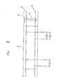
- a vehicle 1 runs on two rails 2 and 3 in the direction indicated by the arrow.
- the rails 2 and 3 are divided into a plurality of sections such as a specific section 4 and a section 5 rear with respect to the direction of advance of the vehicle.
- a transmission signal which is an alternating current reference voltage VQ (this signal is simultaneously fed to the reception side and acts as a local signal St ) is applied to the rails of each of the block sections 4 and 5.
- the rails 2 and 3 are utilized as parts of the circuit and the voltage Vt between the rails 2 and 3 is put out as a track signal St for reception.
- This circuit is known as the alternating current track circuit.
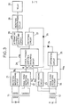
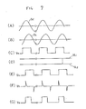
- the transmission signal of the track is a sine wave alternating current signal shown in Fig. 7-A and is put in a rectifying smoothening circuit 21 and a wave form rectifying circuit 22 through a transformer 11.
- the rectifying smoothening circuit 21 is a known circuit for rectifying and smoothening an alternating current signal and forming a direct current output power source Vs.
- the wave form rectifying circuit 22 acts as the first phase judgement signal generating means and is a known circuit, for example, a Schmitt circuit for rectifying a sine wave local signal to a rectangular wave as shown in Fig. 7-C. By these circuits, a rectangular wave phase judgement signal vibrating with the reference voltage level being as the center is obtained.
- the track signal St is put in a level judging signal 23 and a wave form rectifying circuit 24 through a second transformer 12.
- the level judging circuit 23 is a circuit for detecting whether or not a voltage obtained by transforming the track signal St by the transformer 12 acting as the level judgement signal generating means, that is , a level judging signal, is higher than a predetermined value.
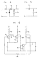
- this circuit comprises a level detecting circuit such as a Schmitt circuit and a known voltage doubling half-wave rectifying circuit for rectifying the output of this detecting circuit, which includes, for example, capacitors C1 and C2 and diodes Dl and D2, as shown in Fig. 4.
- a relatively high threshold level is set in the Schmitt circuit.
- the voltage doubling half-wave rectifying circuit rectifies and smoothens the alternating current voltage put out from the Schmitt circuit by the diode D2 and the capacitor C2 through the coupling capacitor Cl and the clamp diode Dl and a rectified output is obtained from an output terminal D.
- the voltage doubling half-wave rectifying circuit has such a fail-safe structure that at the time of a trouble such as disconnection, no rectified output is obtained (a known four-terminal capacitor which generates no output at the time of disconnection of a terminal is shown as the capacitor C2).
- the direct current voltage Vs of the rectifying smoothening circuit 21 is put in the rectifying circuit.
- the diode Dl is constructed so that a computing oscillator of the subsequent stage is oscillated by the output of the rectifying circuit by clamping the input signal from the capacitor Cl to this input power source Vs.
- the wave form rectifying circuit 24 has a threshold level sufficiently lower than the track signal St put in the circuit 24. Accordingly, a wave-rectified output which changes substantially at the zero point of the track signal St can be produced.
- a differential circuit 25 comprises, for example, a capacitor C3 and a resistor Rl, as shown in Fig. 5, and has such a known structure that the reference voltage level is set at the above-mentioned level Vs. Thus, the phase of the track signal is generated substantially at the zero point (reference voltage level).
- the phase signal of the track signal only a positive signal is put into an input terminal C of a three-input logical product circuit 26 through a diode D4.
- a structure capable of performing a desired operation may be formed even by omitting the diode D4.
- the logical product circuit 26 has three input terminals a, b and c, and this circuit receives the output of the wave form rectifying circuit 22 at the input terminal a and the output of the level detecting circuit 23 at the input terminal b.
- the logical product circuit 26 is a logical product computing oscillating circuit shown in Fig.
- the logical product computing oscillating circuit generates an oscillating output when all of the inputs at the input terminals a, b and c are higher than the power source voltage Vs and has a fail-safe structure in which when a constituent element of the circuit gets out of order, oscillation is impossible and therefore, no output is generated at the time of a trouble,
- the type of the transistor is changed to NPN from PNP and the direction of the diode is reversed.
- Transistors Trl and Tr2 are connected to each other through an attenuation resistor R6, and the collector of the transistor Tr2 is connected to the base of a transistor Tr3 through a level shifting Zener diode ZD1 and the connecting point between a Zener diode ZD2 connected to the collector of the transistor Tr3 and a resistor R4 is connected to the base of the transistor Trl through a resistor R5.
- R2 and R3 represent collector resistors
- R7 represents a resistor on the leak current side, that is, a resistor for flowing of a leak current of the base of the transistor Tr3
- Vs represents an input power source
- C represents an output terminal.
- the operation of the transistors Trl through Tr3 is not reversed and the oscillation is stopped. Also when a trouble such as disconnection is caused in the circuit, the oscillation is stopped and no oscillating output is generated at the output terminal C.
- the Zener voltages VSD1 and VZD2 of the Zener diodes ZDl and V Z D2 of the Zener diodes ZD1 and ZD2 be selected to satisfy the condition of VZD2 ⁇ Vs ⁇ VZD1.
- a computing oscillator of a high output can be constructed by connecting a known amplifier to the input terminal.
- the level judging circuit 23 and the rectifying circuit 27 described hereinafter may comprise, for example, the. voltage doubling half-wave rectifying circuit, and this voltage doubling half-wave rectifying circuit and the the logical product computing oscillator shown in Fig. 6 may be a known fail-safe logical product circuit in which no output is produced unless input signals are applied to all of the input terminals a, b and c, disclosed in, for example, Japanese Utility Model Application Laid-Open Specification No. 4764/82 or Japanese Patent Publication No. 38211/76.
- the rectified output of the rectifying circuit 27 for rectifying the output of the logical product computing oscillating circuit 26 is fed back to the input terminal c, in which the output of the differential circuit 25 is put, through the diode D3.
- An alternating current amplifying circuit 28 amplifies the oscillating output of the logical product computing oscillating circuit 26, and the amplified output is rectified by a rectifying smoothening circuit 29 to drive a trade relay 30, as in the conventional apparatus.
- the above-mentioned transformer 12, wave form rectifying circuit 24, differential circuit 25, rectifying circuit 27 and diodes D3 and D4 constitute the second phase judgement signal generating means, and the wave rectifying circuit 24 and differential circuit 25 constitute the means for detecting the zero point of the track signal.
- the alternating current local signal shown in Fig. 7-A is put in the rectifying smoothening circuit 21 and wave form rectifying circuit 22 through the first transformer 11.
- the rectifying smoothening circuit 21 there is generated the direct current output Vs to be used as the power for driving the level detecting circuit 23, wave form rectifying circuits 22 and 24, amplifying circuit 28, logical product computing oscillating circuit 26 and track relay 30.
- a rectangular wave shown in Fig. 7-C is generated as the phase judging signal. This phase judging signal oscillates with the reference voltage level (corresponding to the zero point of the track signal) being as the center.
- the track signal St put in the second transformer 12 form the rails 2 and 3 has a shape of a sine save as shown in Fig. 7-B.
- the track signal St is put in the level judging circuit 23 and wave form rectifying circuit 24, and a rectified direct current output VL1 for detecting a level higher than a predetermined value, as shown in Fig. 7-D, is produced from the former circuit.
- a rectangular wave as shown in Fig. 7-E is put out from the latter circuit and a differential pulse as shown in Fig. 7-F is put out from the differential circuit 25.
- each of the outputs of the wave form rectifying circuits 22 and 24, level judging circuit 23 and differential circuit 25 is put out in the state where the direct current output Vs of the rectifying smoothening circuit 21 is over-lapped.
- each of positive pulses of the wave rectifying circuit 22, level judging circuit 23 and differential circuit 25 to be put into the input terminals a, b and c of the logical product computing oscillating circuit 26, respectively, has an input level higher than the power source voltage Vs at which initiation of the oscillation is possible,
- the phase judgement condition (the local signal and the track signal are of the same phase) is established (first logical product)
- the logical product (second logical product) of this established condition and the already established level judgement condition (the voltage level of the track signal is higher than a predetermined value) is established and oscillation is initiated in the logical product computing oscillating circuit 26.
- the oscillating output of the computing oscillating circuit 26 is put in the alternating current amplifying circuit 28 and is simultaneously rectified by the rectifying circuit 27 and fed back to the input terminal c through the diode D3 to self-retain the output of the computing oscillator 26 until the phase signal on the local signal side (Fig. 7-C) falls, whereby amplification of the pulse width is effected (see Fig. 7-G).
- the diode D3 prevents extinction of the differential pulse at the capacitor C 2 of the rectifying circuit 27.
- the pulse width-amplified output, shown in Fig. 7-G, of the computing oscillating circuit 26 is amplified by the alternating amplifying circuit 28, rectified by the rectifying smoothening circuit 29 and supplied to the relay 30 to retain the relay 30 in the excited state. Namely, the absence of a train in the track circuit is informed.
- the track signal St put out from the wave rectifying circuit 24 is differentiated and the positive differential pulse is put in the computing oscillating circuit 26, whereby the oscillating output is self-retained and maintained.
- the phase to be judged is simultaneously determined.
- the judged value of the phase is changed with this change of the voltage level. This change becomes great as the set value for th- judgement of the level is large.
- the conventional apparatus is disadvantageous in that if increase of the precision of the level judgement is intended, the precision of the phase judgement is reduced and if maintenance of a high precision of the phase judgement is intended, the precision of the level judgement is reduced.
- the set value for the level judgement can be increased, and the phase judgement can always be done at the point where the phase judging signal crosses the reference voltage, that is, at the point (zero point) where the track signal is changed to the positive value from the negative value. Accordingly, the detection precision can be elevated and the reliability can be improved.
- known fail-safe logical product computing oscillating circuit 26, level judging circuit 23, rectifying circuit 27, alternating current amplifying circuit 28 and differential circuit 25 are used, a fail-safe structure is realized in the detecting apparatus.
- the computing oscillating circuit 26 is not self-retained if the diode D3 is opened, a power sufficient to excite the relay 30 is not obtained, and since the differential pulse is absorbed in the capacitor C2 and no signal is put in the input terminal c of the computing oscillating circuit 26 if a short circuit is formed, a fail-safe effect is attained.
- the logical product of the level judgement and the phase judgement is made by one logical product circuit, but the present invention is not limited to this structure. Namely, there may be adopeted a structure in which the phase judgement is carried out by using a fail-safe logical product circuit, the relay 30 is driven by this judgement signal and the contact output of the relay driven by the output of the level judging circuit 23 is connected in series to the contact output of the relay 30.
- the rectifying circuit is used as the level judging circuit 23, it is obvious that the output may be rectified by using a known level detector of the alternating current input type.
- the input level of the track signal is stable, it is obvious that an alternating current output from the level detecting circuit of the level judging circuit 23, as indicated by a dot line in Fig. 3, can be utilized instead of the wave rectifying circuit 24. Furthermore, if the input detection level of the logical product circuit is made equal to the judgement level of the track signal, the logical product circuit can be utilized as the level judging circuit 23. In this case, it is sufficient if the level judging circuit 23 is replaced by a rectifying circuit.
- the capacity of the smoothening capacitor C2 of the interposed rectifying circuit can be increased, whereby an erroneous operation by a noise of the track signal or the like can be moderated.
- the local input signal is rectified to obtain a direct current power and precise and various level detections can be performed by this direct current power, and the logical computation is carried out as the logical processing of the output of such level detection and such processing can be integrated, whereby the size of the apparatus can be reduced. Moreover, when the apparatus gets out of order, the output is inevitably reduced to zero and the relay falls to the safe side, and a fail-safe effect can be assuredly attained.
- phase judgement can be made at a voltage level close to the reference level while the level judgement can be made at a voltage level higher than a predetermined value, and precise phase judgement and level judgement become possible.
- the apparatus for detecting a vehicle on a track is most effectively utilized for detecting a train on a rails in a signal system of a railroad line or in an unmanned operation system in a factory, a dockyard or an assorting or marshaling yard.
Landscapes
- Engineering & Computer Science (AREA)
- Automation & Control Theory (AREA)
- Mechanical Engineering (AREA)
- Train Traffic Observation, Control, And Security (AREA)
Abstract
Applications Claiming Priority (1)
| Application Number | Priority Date | Filing Date | Title |
|---|---|---|---|
| PCT/JP1986/000508 WO1988002326A1 (fr) | 1986-10-03 | 1986-10-03 | Detecteur de vehicules sur une piste |
Publications (3)
| Publication Number | Publication Date |
|---|---|
| EP0288564A1 true EP0288564A1 (fr) | 1988-11-02 |
| EP0288564A4 EP0288564A4 (fr) | 1989-06-21 |
| EP0288564B1 EP0288564B1 (fr) | 1999-01-20 |
Family
ID=13874550
Family Applications (1)
| Application Number | Title | Priority Date | Filing Date |
|---|---|---|---|
| EP86905931A Expired - Lifetime EP0288564B1 (fr) | 1986-10-03 | 1986-10-03 | Detecteur de vehicules sur une piste |
Country Status (3)
| Country | Link |
|---|---|
| EP (1) | EP0288564B1 (fr) |
| DE (1) | DE3650708T2 (fr) |
| WO (1) | WO1988002326A1 (fr) |
Cited By (1)
| Publication number | Priority date | Publication date | Assignee | Title |
|---|---|---|---|---|
| WO1991011356A1 (fr) * | 1990-01-25 | 1991-08-08 | Eb Signal Ab | Systeme de circuit de voie |
Family Cites Families (6)
| Publication number | Priority date | Publication date | Assignee | Title |
|---|---|---|---|---|
| FR1258776A (fr) * | 1960-06-08 | 1961-04-14 | Siemens Ag | Installation pour l'exploitation de tensions alternatives par comparaison à une tension de référence en particulier pour le service de sécurité des chemins de fer |
| DE2047147A1 (de) * | 1970-09-24 | 1972-03-30 | Sel | Einrichtung zum Überwachen von Gleisabschnitten für Eisenbahnverkehrs anlagen |
| FR2214620B1 (fr) * | 1973-01-19 | 1975-04-04 | Jeumont Schneider | |
| US4065081A (en) * | 1976-12-09 | 1977-12-27 | General Signal Corporation | Alternating current track circuits |
| US4417229A (en) * | 1980-10-15 | 1983-11-22 | Safetran Systems Corporation | Means for use on a railroad to distinguish between traction current and signal current |
| IT1150556B (it) * | 1981-06-26 | 1986-12-17 | Sasib Spa | Rele statico di binario in corrente alternata |
-
1986
- 1986-10-03 WO PCT/JP1986/000508 patent/WO1988002326A1/fr not_active Ceased
- 1986-10-03 DE DE3650708T patent/DE3650708T2/de not_active Expired - Fee Related
- 1986-10-03 EP EP86905931A patent/EP0288564B1/fr not_active Expired - Lifetime
Cited By (1)
| Publication number | Priority date | Publication date | Assignee | Title |
|---|---|---|---|---|
| WO1991011356A1 (fr) * | 1990-01-25 | 1991-08-08 | Eb Signal Ab | Systeme de circuit de voie |
Also Published As
| Publication number | Publication date |
|---|---|
| EP0288564B1 (fr) | 1999-01-20 |
| EP0288564A4 (fr) | 1989-06-21 |
| DE3650708D1 (de) | 1999-03-04 |
| DE3650708T2 (de) | 1999-07-01 |
| WO1988002326A1 (fr) | 1988-04-07 |
Similar Documents
| Publication | Publication Date | Title |
|---|---|---|
| US4525699A (en) | Electronic monitoring system with malfunction indicator | |
| US3696243A (en) | Broken rail detector | |
| JP2720107B2 (ja) | 鉄道信号システム | |
| US3736434A (en) | Fail-safe electronic comparator circuit | |
| US3553488A (en) | Fail-safe circuit arrangement | |
| KR910010899A (ko) | 다중 통로 반사 방해에 의한 영향에 신속 대응 가능한 수신기 장치 | |
| US5617308A (en) | Noise-immune, clamped, resonant link inverter | |
| EP0288564A1 (fr) | Detecteur de vehicules sur une piste | |
| US2993116A (en) | Electronic track circuit | |
| JP3819807B2 (ja) | 絶縁駆動型インバータ装置 | |
| US20140340080A1 (en) | Wireless proximity switch with a target device comprising an inverter | |
| EP0981196A2 (fr) | Alimentation de puissance pour compresseur vibrant | |
| US3752426A (en) | Train detector | |
| US3529150A (en) | Electronic track circuit for railway signalling | |
| KR830001844B1 (ko) | 차량의 기계 동작을 감지하는 장치 | |
| US3617836A (en) | Control circuit for synchronous motor | |
| US6897719B2 (en) | Demodulation circuit and demodulation method | |
| US3351945A (en) | Safety remote control for a carrier | |
| JPH0678062B2 (ja) | 列車検知装置 | |
| JP2934085B2 (ja) | 列車検知装置 | |
| US4056739A (en) | Fail-safe electronic polarized relay | |
| US3462614A (en) | Frequency selective circuit with output according to a ratio of alternating current signals-to-direct current signals which varies with frequency | |
| JP3588707B2 (ja) | 波形整形回路 | |
| JPS6260032B2 (fr) | ||
| US6232809B1 (en) | Differential input comparator with double sided hysteresis |
Legal Events
| Date | Code | Title | Description |
|---|---|---|---|
| PUAI | Public reference made under article 153(3) epc to a published international application that has entered the european phase |
Free format text: ORIGINAL CODE: 0009012 |
|
| 17P | Request for examination filed |
Effective date: 19870413 |
|
| AK | Designated contracting states |
Kind code of ref document: A1 Designated state(s): DE GB |
|
| A4 | Supplementary search report drawn up and despatched |
Effective date: 19890621 |
|
| 17Q | First examination report despatched |
Effective date: 19910513 |
|
| GRAG | Despatch of communication of intention to grant |
Free format text: ORIGINAL CODE: EPIDOS AGRA |
|
| GRAG | Despatch of communication of intention to grant |
Free format text: ORIGINAL CODE: EPIDOS AGRA |
|
| GRAH | Despatch of communication of intention to grant a patent |
Free format text: ORIGINAL CODE: EPIDOS IGRA |
|
| GRAH | Despatch of communication of intention to grant a patent |
Free format text: ORIGINAL CODE: EPIDOS IGRA |
|
| GRAA | (expected) grant |
Free format text: ORIGINAL CODE: 0009210 |
|
| AK | Designated contracting states |
Kind code of ref document: B1 Designated state(s): DE GB |
|
| REF | Corresponds to: |
Ref document number: 3650708 Country of ref document: DE Date of ref document: 19990304 |
|
| PG25 | Lapsed in a contracting state [announced via postgrant information from national office to epo] |
Ref country code: DE Free format text: LAPSE BECAUSE OF FAILURE TO SUBMIT A TRANSLATION OF THE DESCRIPTION OR TO PAY THE FEE WITHIN THE PRESCRIBED TIME-LIMIT Effective date: 19990421 |
|
| PLBE | No opposition filed within time limit |
Free format text: ORIGINAL CODE: 0009261 |
|
| STAA | Information on the status of an ep patent application or granted ep patent |
Free format text: STATUS: NO OPPOSITION FILED WITHIN TIME LIMIT |
|
| 26N | No opposition filed | ||
| REG | Reference to a national code |
Ref country code: GB Ref legal event code: IF02 |
|
| PGFP | Annual fee paid to national office [announced via postgrant information from national office to epo] |
Ref country code: GB Payment date: 20020926 Year of fee payment: 17 |
|
| PGFP | Annual fee paid to national office [announced via postgrant information from national office to epo] |
Ref country code: DE Payment date: 20021028 Year of fee payment: 17 |
|
| PG25 | Lapsed in a contracting state [announced via postgrant information from national office to epo] |
Ref country code: GB Free format text: LAPSE BECAUSE OF NON-PAYMENT OF DUE FEES Effective date: 20031003 |
|
| GBPC | Gb: european patent ceased through non-payment of renewal fee |
Effective date: 20031003 |