EP0287525A2 - Einschaltstromrückführung durch einen eine induktive Last treibenden Leistungsschalttransistor - Google Patents
Einschaltstromrückführung durch einen eine induktive Last treibenden Leistungsschalttransistor Download PDFInfo
- Publication number
- EP0287525A2 EP0287525A2 EP88830137A EP88830137A EP0287525A2 EP 0287525 A2 EP0287525 A2 EP 0287525A2 EP 88830137 A EP88830137 A EP 88830137A EP 88830137 A EP88830137 A EP 88830137A EP 0287525 A2 EP0287525 A2 EP 0287525A2
- Authority
- EP
- European Patent Office
- Prior art keywords
- transistor
- circuit
- diode
- inductive load
- power switching
- Prior art date
- Legal status (The legal status is an assumption and is not a legal conclusion. Google has not performed a legal analysis and makes no representation as to the accuracy of the status listed.)
- Granted
Links
Images
Classifications
-
- H—ELECTRICITY
- H03—ELECTRONIC CIRCUITRY
- H03K—PULSE TECHNIQUE
- H03K17/00—Electronic switching or gating, i.e. not by contact-making and –breaking
- H03K17/08—Modifications for protecting switching circuit against overcurrent or overvoltage
- H03K17/082—Modifications for protecting switching circuit against overcurrent or overvoltage by feedback from the output to the control circuit
- H03K17/0826—Modifications for protecting switching circuit against overcurrent or overvoltage by feedback from the output to the control circuit in bipolar transistor switches
Definitions
- the present invention relates to electronic circuits for driving inductive loads utilizing semiconductor power devices to drive the load and, more particularly circuits of this type monolithically integrated.
- a first solution contemplates connecting a recirculation diode across the inductive load to provide a recirculation path to the current for discharging the stored energy.
- Another solution contemplates recirculating the discharge current of the energy stored in the inductive load through the same power switching transistor, by connecting a control Zener diode between the base and the collector of the power transistor;
- the first solution has the disadvantage of requiring at least an additional power device, i.e. the recirculation diode, adequately dimensioned to withstand the passage of the peak discharge current.
- the second solution although using advantageously the same driving power transistor for recirculating the discharge current, requires the control Zener diode to be designed case by case in function of the supply voltage of the circuit in order not to interfere during the charging phase of the inductance.
- the present invention proposes a new and advantageous circuit which, differently from the circuits of the prior art, does not require the use of an additional power device for functionally recirculating the discharge current while being at the same time substantially adapted to whatever supply voltage is utilized by the circuit.
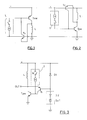
- the inductive load is indicated with L
- the power switching transistor is indicated with Tpw
- the drive circuit is complessively shown by the elements drawn inside the dash line block indicated with 1.
- the circuit of the invention contemplates the use of a control transistor Tc (NPN) of opposite polarity in respect to that of the power transistor Tpw (PNP).
- the emitter of the control transistor Tc is connected in common to the collector of the power transistor Tpw, the collector of the control transistor Tc is connected to the base of the power transistor and the base of the control transistor is connected to the ground node of the circuit.
- Fig. 2 Substantially analogous is the circuit depicted in Fig. 2 made with devices of opposite polarity, i.e. an NPN power transistor Tpw and a PNP control transistor Tc. Essentially the circuits of Fig. 1 and of Fig. 2 operate as follows.
- a negative (Fig. 1) or a positive (Fig. 2) overvoltage develops across the inductance L.
- this voltage reaches a value corresponding to the value of one VBE, the control transistor Tc turns-on and drives to conduction the power transistor Tpw.
- the control transistor Tc withstands a minimum fraction of the discharge current of the energy stored in the inductance L (i.e. a fraction equal to 1/ of the discharge current, being the current gain of the control transistor Tc) and therefore it may be a transistor of relatively small size.
- An advantage of this circuit in respect to the known circuits is that of allowing recirculation of the discharge current from the inductive load through the power transistor Tpw at a voltage equal essentially to the supply voltage plus an overvoltage which, independently of the actual value of the supply voltage, is limited to the value of one VBE without requiring the use of a recirculation power device.
- recirculation of the discharge current of the inductance may also be conducted at incrementally increased voltages (increased by a multiple number (n) of VBE), if so desired by inserting (n) diodes or (n) Zener diodes in series between the collector of the power transistor Tpw and the emitter of the control transistor of opposite polarity Tc.
- the circuit of the invention remains unable to limit the maximum absolute value of the total voltage at which recirculation through the power transistor Tpw of the discharge current from the inductive load takes place, should an anomalous increase of the supply voltage (e.g. caused by a dumping effect) be concomitant with the switching off of the current through the load. Under these accidental circumstances the power device Tpw may be subjected to an excessive voltage.
- the circuit of the invention may be modified in order to make the circuit capable of obviating also to this additive problem, through the addition of a secondary recirculation means which is brought into conduction by the raising of the supply voltage above a pre-set value and determining, in all instances, the turning-on of the power transistor.
- Such a modified embodiment of the circuit of the invention is shown in Fig. 3.
- the operation of the circuit may be described as follows.
- a positive overvoltage across the inductance L develops.
- this overvoltage reaches the value corresponding to VAL + VBE Tc + VBE D1 (where VAL is the supply voltage)
- the power device Tpw turns-on again because of the turning-on of the PNP control transistor Tc which acts as a driver.
- the maximum recirculation voltage affecting the power transistor Tpw may be conveniently limited thus positively preventing the power device Tpw from being subjected to destructive voltages even in the presence of high overvoltages on the supply at the instant of interruption of the driving of the power switching transistor.
- the embodiment depicted in Fig. 3 offers the advantage of allowing the adoption of a relatively lower voltage fabrication process because the circuit of the invention provides a reliable protection of the power transistor against breakdown.
- the improved circuit of Fig. 3 maintains the advantage of utilizing substantially a single power device for driving the inductive load as well as for recirculating the discharge current of the load.
- the secondary recirculation means namely the diodes D1, D2 and DZ1, must, in fact, be capable of withstanding a fraction of the recirculation current which flows almost exclusively through the power transistor Tpw.
- circuit of Fig. 3 may be made with devices (transistors) of reverse polarity by inverting all the polarities of the circuit.
Landscapes
- Electronic Switches (AREA)
- Power Conversion In General (AREA)
Applications Claiming Priority (4)
| Application Number | Priority Date | Filing Date | Title |
|---|---|---|---|
| IT8361887 | 1987-04-14 | ||
| IT8783618A IT1214240B (it) | 1987-04-14 | 1987-04-14 | Ricircolo della corrente di un carico induttivo attraverso lo stesso dispositivo di potenza di pilotaggio. |
| IT8363987 | 1987-06-30 | ||
| IT8783639A IT1214250B (it) | 1987-06-30 | 1987-06-30 | Ricircolo della correnta di un carico induttivo attraverso lo stesso dispositivo di potenza di pilotaggio ad una tensione massima limitata prestabilita'. |
Publications (3)
| Publication Number | Publication Date |
|---|---|
| EP0287525A2 true EP0287525A2 (de) | 1988-10-19 |
| EP0287525A3 EP0287525A3 (en) | 1988-11-17 |
| EP0287525B1 EP0287525B1 (de) | 1992-06-10 |
Family
ID=26330098
Family Applications (1)
| Application Number | Title | Priority Date | Filing Date |
|---|---|---|---|
| EP88830137A Expired EP0287525B1 (de) | 1987-04-14 | 1988-03-30 | Einschaltstromrückführung durch einen eine induktive Last treibenden Leistungsschalttransistor |
Country Status (4)
| Country | Link |
|---|---|
| US (1) | US4962346A (de) |
| EP (1) | EP0287525B1 (de) |
| JP (1) | JP2911453B2 (de) |
| DE (1) | DE3871846T2 (de) |
Cited By (4)
| Publication number | Priority date | Publication date | Assignee | Title |
|---|---|---|---|---|
| GB2281667A (en) * | 1993-09-04 | 1995-03-08 | Bosch Gmbh Robert | Fuel injector driver control circuit |
| EP0660519A2 (de) * | 1993-12-23 | 1995-06-28 | Lucas Industries Public Limited Company | Halbleitervorrichtungsschutzschaltung |
| EP0893749A1 (de) * | 1997-07-18 | 1999-01-27 | Ansaldo Sistemi Industriali S.p.A. | Elektronischer Schaltkreis zur Transientenminderung beim Einschalten |
| EP3232571A1 (de) * | 2016-04-14 | 2017-10-18 | Nexperia B.V. | Festkörperrelais |
Families Citing this family (5)
| Publication number | Priority date | Publication date | Assignee | Title |
|---|---|---|---|---|
| US5210675A (en) * | 1989-07-11 | 1993-05-11 | Sgs-Thomson Microelectronics S.R.L. | Circuit for protection against negative overvoltages across the power supply of an integrated circuit comprising a power device with related control circuit |
| US5508906A (en) * | 1993-01-04 | 1996-04-16 | Motorola, Inc. | Low loss recirculation apparatus |
| US5625518A (en) * | 1995-12-04 | 1997-04-29 | Ford Motor Company | Clamping circuit with reverse polarity protection |
| JP3443591B2 (ja) * | 1996-09-24 | 2003-09-02 | ローム株式会社 | コイル負荷駆動回路 |
| DE19838109B4 (de) * | 1998-08-21 | 2005-10-27 | Infineon Technologies Ag | Ansteuerschaltung für induktive Lasten |
Citations (4)
| Publication number | Priority date | Publication date | Assignee | Title |
|---|---|---|---|---|
| DE2423258A1 (de) * | 1974-05-14 | 1976-02-05 | Siemens Ag | Schaltungsanordnung zur stromversorgung eines induktiven verbrauchers |
| DE2638178A1 (de) * | 1976-08-25 | 1978-03-02 | Bosch Gmbh Robert | Schutzvorrichtung fuer elektronische schaltungen gegen ueberspannungen |
| US4287436A (en) * | 1978-06-07 | 1981-09-01 | Tokyo Shibaura Denki Kabushiki Kaisha | Electrical circuit for driving an inductive load |
| JPS595747A (ja) * | 1982-06-30 | 1984-01-12 | Mitsubishi Electric Corp | コイル駆動回路 |
Family Cites Families (11)
| Publication number | Priority date | Publication date | Assignee | Title |
|---|---|---|---|---|
| US3435295A (en) * | 1966-09-28 | 1969-03-25 | Mohawk Data Sciences Corp | Integrated power driver circuit |
| US3676713A (en) * | 1971-04-23 | 1972-07-11 | Ibm | Saturation control scheme for ttl circuit |
| JPS5083953U (de) * | 1973-12-07 | 1975-07-18 | ||
| US3978350A (en) * | 1975-03-11 | 1976-08-31 | Nasa | Dual mode solid state power switch |
| US4035670A (en) * | 1975-12-24 | 1977-07-12 | California Linear Circuits, Inc. | Transistor stored charge control using a recombination layer diode |
| US4055794A (en) * | 1976-05-10 | 1977-10-25 | Rohr Industries, Incorporated | Base drive regulator |
| FR2361777A1 (fr) * | 1976-08-14 | 1978-03-10 | Bosch Gmbh Robert | Montage pour deriver le courant de coupure d'un appareil utilisateur inductif |
| DE2852943C3 (de) * | 1978-12-07 | 1981-09-10 | Licentia Patent-Verwaltungs-Gmbh, 6000 Frankfurt | Anordnung mit einem verzögerungsbehafteten Halbleiterschalter |
| JPS5833322A (ja) * | 1981-08-21 | 1983-02-26 | Toshiba Corp | トランジスタ回路 |
| JPS5855582B2 (ja) * | 1981-11-13 | 1983-12-10 | 株式会社東芝 | 透視性テ−プカセツト |
| US4639823A (en) * | 1983-12-27 | 1987-01-27 | Fuji Electric Co., Ltd. | Control circuit for switching transistors |
-
1988
- 1988-03-30 DE DE8888830137T patent/DE3871846T2/de not_active Expired - Fee Related
- 1988-03-30 EP EP88830137A patent/EP0287525B1/de not_active Expired
- 1988-04-12 US US07/180,501 patent/US4962346A/en not_active Expired - Lifetime
- 1988-04-13 JP JP63091215A patent/JP2911453B2/ja not_active Expired - Fee Related
Patent Citations (4)
| Publication number | Priority date | Publication date | Assignee | Title |
|---|---|---|---|---|
| DE2423258A1 (de) * | 1974-05-14 | 1976-02-05 | Siemens Ag | Schaltungsanordnung zur stromversorgung eines induktiven verbrauchers |
| DE2638178A1 (de) * | 1976-08-25 | 1978-03-02 | Bosch Gmbh Robert | Schutzvorrichtung fuer elektronische schaltungen gegen ueberspannungen |
| US4287436A (en) * | 1978-06-07 | 1981-09-01 | Tokyo Shibaura Denki Kabushiki Kaisha | Electrical circuit for driving an inductive load |
| JPS595747A (ja) * | 1982-06-30 | 1984-01-12 | Mitsubishi Electric Corp | コイル駆動回路 |
Non-Patent Citations (1)
| Title |
|---|
| PATENT ABSTRACTS OF JAPAN, vol. 8, no. 84 (E-239)[1521], 18th April 1984; & JP-A-59 005 747 (MITSUBISHI DENKI K.K.) 12-01-1984 * |
Cited By (9)
| Publication number | Priority date | Publication date | Assignee | Title |
|---|---|---|---|---|
| GB2281667A (en) * | 1993-09-04 | 1995-03-08 | Bosch Gmbh Robert | Fuel injector driver control circuit |
| GB2281667B (en) * | 1993-09-04 | 1997-11-19 | Bosch Gmbh Robert | Drive control of an electromagnetic load |
| EP0660519A2 (de) * | 1993-12-23 | 1995-06-28 | Lucas Industries Public Limited Company | Halbleitervorrichtungsschutzschaltung |
| EP0660519B1 (de) * | 1993-12-23 | 2001-08-22 | Lucas Industries Limited | Halbleitervorrichtungsschutzschaltung |
| EP0893749A1 (de) * | 1997-07-18 | 1999-01-27 | Ansaldo Sistemi Industriali S.p.A. | Elektronischer Schaltkreis zur Transientenminderung beim Einschalten |
| US6060868A (en) * | 1997-07-18 | 2000-05-09 | Ansaldo Sistemi Industriali S.P.A. | Electronic switching circuit for reducing power-on switching transients |
| EP3232571A1 (de) * | 2016-04-14 | 2017-10-18 | Nexperia B.V. | Festkörperrelais |
| US10972074B2 (en) | 2016-04-14 | 2021-04-06 | Nexperia B.V. | Solid state relay |
| EP4096095A1 (de) * | 2016-04-14 | 2022-11-30 | Nexperia B.V. | Festkörperrelais |
Also Published As
| Publication number | Publication date |
|---|---|
| DE3871846D1 (de) | 1992-07-16 |
| JPS63272221A (ja) | 1988-11-09 |
| EP0287525A3 (en) | 1988-11-17 |
| DE3871846T2 (de) | 1993-02-04 |
| JP2911453B2 (ja) | 1999-06-23 |
| EP0287525B1 (de) | 1992-06-10 |
| US4962346A (en) | 1990-10-09 |
Similar Documents
| Publication | Publication Date | Title |
|---|---|---|
| US5200878A (en) | Drive circuit for current sense igbt | |
| EP0206505B1 (de) | Überstromschutzschaltung für MOSFET mit Leitfähigkeitsmodulation | |
| US5352932A (en) | Trigger circuit for a power FET with a load on the source side | |
| US4217618A (en) | Thyristor firing circuit module with integral optical isolation, dv/dt limitation, and bidirectional voltage transient suppression | |
| EP0437108B1 (de) | Steuerschaltung zum Schalten eines Stromes in einer Last | |
| US5010439A (en) | Control circuit for the clamping voltage of an inductive load driven by a power device in a high side driver configuration | |
| US4215279A (en) | Apparatus for controlling the operation of power transistors in a switching mode | |
| US4642746A (en) | Circuit arrangement for feeding the regulation and control device of a regulated direct voltage converter | |
| US4723191A (en) | Electronic voltage regulator for use in vehicles with protection against transient overvoltages | |
| US4962346A (en) | Transitory current recirculation through a power switching transistor driving an inductive load | |
| US6255890B1 (en) | Circuit for controlling the switching of a load by means of an emitter-switching device | |
| US4564769A (en) | Saturation control of a switching transistor | |
| EP0216816B1 (de) | Schaltung zum ableiten gespeicherter induktiver energie | |
| US4904889A (en) | Circuit for driving electronic devices with a low supply voltage | |
| US4410809A (en) | Static induction transistor gate driving circuit | |
| US4893212A (en) | Protection of power integrated circuits against load voltage surges | |
| US4902921A (en) | Drive circuit for driving cascode bipolar-MOS circuit | |
| US4224654A (en) | Relay driver circuit | |
| US5945868A (en) | Power semiconductor device and method for increasing turn-on time of the power semiconductor device | |
| US4456836A (en) | Gate circuit for gate turn-off thyristor | |
| JPH051652B2 (de) | ||
| US5495198A (en) | Snubbing clamp network | |
| EP0425024B1 (de) | Schaltung zum Begrenzen der Ausgangsspannung einer eine mit der Versorgungsspannung verbundene resonante Last treibenden monolithischen Halbleiterleistungsvorrichtung | |
| EP0715409B1 (de) | Schaltung zur Begrenzung der Ausgangsspannung eines Leistungstransistors | |
| EP0220791A1 (de) | Schalteinrichtung |
Legal Events
| Date | Code | Title | Description |
|---|---|---|---|
| PUAI | Public reference made under article 153(3) epc to a published international application that has entered the european phase |
Free format text: ORIGINAL CODE: 0009012 |
|
| PUAL | Search report despatched |
Free format text: ORIGINAL CODE: 0009013 |
|
| AK | Designated contracting states |
Kind code of ref document: A2 Designated state(s): DE FR GB |
|
| AK | Designated contracting states |
Kind code of ref document: A3 Designated state(s): DE FR GB |
|
| 17P | Request for examination filed |
Effective date: 19890214 |
|
| RAP1 | Party data changed (applicant data changed or rights of an application transferred) |
Owner name: SGS-THOMSON MICROELECTRONICS S.R.L. |
|
| 17Q | First examination report despatched |
Effective date: 19900719 |
|
| GRAA | (expected) grant |
Free format text: ORIGINAL CODE: 0009210 |
|
| AK | Designated contracting states |
Kind code of ref document: B1 Designated state(s): DE FR GB |
|
| ET | Fr: translation filed | ||
| REF | Corresponds to: |
Ref document number: 3871846 Country of ref document: DE Date of ref document: 19920716 |
|
| PLBE | No opposition filed within time limit |
Free format text: ORIGINAL CODE: 0009261 |
|
| STAA | Information on the status of an ep patent application or granted ep patent |
Free format text: STATUS: NO OPPOSITION FILED WITHIN TIME LIMIT |
|
| 26N | No opposition filed | ||
| REG | Reference to a national code |
Ref country code: FR Ref legal event code: D6 |
|
| REG | Reference to a national code |
Ref country code: GB Ref legal event code: IF02 |
|
| PGFP | Annual fee paid to national office [announced via postgrant information from national office to epo] |
Ref country code: FR Payment date: 20020312 Year of fee payment: 15 |
|
| PGFP | Annual fee paid to national office [announced via postgrant information from national office to epo] |
Ref country code: GB Payment date: 20020327 Year of fee payment: 15 |
|
| PGFP | Annual fee paid to national office [announced via postgrant information from national office to epo] |
Ref country code: DE Payment date: 20020404 Year of fee payment: 15 |
|
| PG25 | Lapsed in a contracting state [announced via postgrant information from national office to epo] |
Ref country code: GB Free format text: LAPSE BECAUSE OF NON-PAYMENT OF DUE FEES Effective date: 20030330 |
|
| PG25 | Lapsed in a contracting state [announced via postgrant information from national office to epo] |
Ref country code: DE Free format text: LAPSE BECAUSE OF NON-PAYMENT OF DUE FEES Effective date: 20031001 |
|
| GBPC | Gb: european patent ceased through non-payment of renewal fee |
Effective date: 20030330 |
|
| PG25 | Lapsed in a contracting state [announced via postgrant information from national office to epo] |
Ref country code: FR Free format text: LAPSE BECAUSE OF NON-PAYMENT OF DUE FEES Effective date: 20031127 |
|
| REG | Reference to a national code |
Ref country code: FR Ref legal event code: ST |