EP0285941B1 - Verfahren zur Herstellung von elektrischen Kontaktwerkstoffen - Google Patents
Verfahren zur Herstellung von elektrischen Kontaktwerkstoffen Download PDFInfo
- Publication number
- EP0285941B1 EP0285941B1 EP88104920A EP88104920A EP0285941B1 EP 0285941 B1 EP0285941 B1 EP 0285941B1 EP 88104920 A EP88104920 A EP 88104920A EP 88104920 A EP88104920 A EP 88104920A EP 0285941 B1 EP0285941 B1 EP 0285941B1
- Authority
- EP
- European Patent Office
- Prior art keywords
- component
- mould
- recesses
- plastics material
- carrier layer
- Prior art date
- Legal status (The legal status is an assumption and is not a legal conclusion. Google has not performed a legal analysis and makes no representation as to the accuracy of the status listed.)
- Expired - Lifetime
Links
Images

Classifications
-
- H—ELECTRICITY
- H01—ELECTRIC ELEMENTS
- H01H—ELECTRIC SWITCHES; RELAYS; SELECTORS; EMERGENCY PROTECTIVE DEVICES
- H01H1/00—Contacts
- H01H1/02—Contacts characterised by the material thereof
- H01H1/021—Composite material
-
- H—ELECTRICITY
- H01—ELECTRIC ELEMENTS
- H01H—ELECTRIC SWITCHES; RELAYS; SELECTORS; EMERGENCY PROTECTIVE DEVICES
- H01H11/00—Apparatus or processes specially adapted for the manufacture of electric switches
- H01H11/04—Apparatus or processes specially adapted for the manufacture of electric switches of switch contacts
Definitions
- the invention relates to a method for producing electrical contact materials according to the preamble of patent claim 1.
- a method of the generic type is known from DE-PS 554720. Relatively large contact surfaces are formed with highly conductive material, so that local overheating can have a negative effect on the erosion resistance and the service life.
- Another such method for the production of flat composite materials from heterogeneous components is known from DE-PS 758108; First, depressions in the form of parallel grooves are made in one material, which are then filled with filler material, e.g. B. metal oxide, powdered graphite, difficult to melt material such as tungsten or conductive material such as silver, resulting in a heterogeneous contact surface. The desired heterogeneity is only achieved in one direction, namely across the filled grooves.
- a sheathed wire whose core is made of a metal of high strength, e.g. B. made of nickel, and its jacket made of a metal with good electrical conductivity, for. B. of silver, consists of repeatedly bundling and stretching, whereupon the fiber bundle thus formed is divided into individual slices transversely to the fiber orientation.
- the contact material formed in this way has good electrical and thermal conductivity due to the silver network, while the nickel cores enclosed by the silver increase the resistance to erosion or reduce the tendency to sweat (see company publication of G. Rau, Pforzheim).
- a disadvantage of this contact material is an uneven material distribution as a result of fluctuations in the nickel core diameter. There is also the risk of fiber breaks due to multiple forming.
- a pore-containing structure is produced by sintering a high-melting metal, into which a low-melting metal is sucked in by capillary forces (A. Keil, WA Merl, E. Vinaricky: “Electrical contacts and their materials", Springer-Verlag, Berlin , Heidelberg, New York, Toyko 1984).
- these contact materials which are produced using the sintering impregnation process, also show large fluctuations in the pore size. This has the result that electrical and thermal conductivity on the one hand and erosion resistance on the other hand change locally, which has a disadvantageous effect on the contact resistance and the contact life.
- material losses due to the waste when parting slices from the bundles or rods must be accepted.
- the invention has for its object a method for producing an electrical contact material in the form of a contact body to create from a heterogeneous composite of two components, in which the lateral, ie transverse to the electrical current flow of the contact body extending distribution and geometry of the two components in the ⁇ m range are freely selectable and can be maintained with high accuracy.
- the respectively desired electrical and mechanical properties of the contact material can be realized without local deviations due to manufacturing tolerances.
- the smallest lateral dimensions of the components can be in the ⁇ m range with a structure height of up to 1 mm.
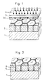
- Figures 1 to 5 schematically illustrate the production of an electrical contact material, consisting of a composite of two components, of which one component has a high hardness and strength and the other component has a high electrical and thermal conductivity.
- Fig. 1 shows in section a metallic carrier layer 1, for. B. made of chromium-nickel steel, on which a resist layer 2 sensitive to X-rays is applied.
- the resist layer 2 is exposed to the extremely parallel radiation 4 from a synchrotron via an X-ray mask 3 with absorber structures 3a.
- the areas of the resist layer 2 that are not shadowed by the absorber structures 3a of the X-ray mask 3 are changed by radiation chemistry.
- a cone-shaped plastic mold 5 (FIG. 2) is produced which corresponds to the absorber structure 3a of the X-ray mask 3 and which has the thickness of the resist layer 2.
- the areas 6 of the plastic mold 5 which are exposed during development are galvanically coated with a metal of high hardness and strength 7, e.g. B. nickel, filled (Fig. 3). After the metallic structure 7 thus formed has been leveled, the remaining plastic (pin) 5 is detached. A coherent, net-shaped metal structure 7 is created with chamber-like depressions 8 (FIG. 4).
- a metal of high hardness and strength 7 e.g. B. nickel
- the metal structure 7 By impregnating the metal structure 7 with a metal whose melting point is lower than the melting points of metals 1 and 7 and which has a high electrical and thermal conductivity, e.g. B. silver, creates a contact material that combines the properties of its two material components.
- the metal structure 7 can be made wettable for the metal with good electrical and thermal conductivity by a dipping process or vapor deposition of a layer. After soaking can the carrier layer 1 are removed.
- Fig. 5 shows this contact material in plan view, consisting of pins made of a material with high electrical and thermal conductivity 9, which are chambered by the reticulated metal structure 7 made of a material of high hardness and strength.
- the carrier layer 1 which in this case does not have to be electrically conductive, can again be removed. If the carrier layer 1 is an electrically conductive contact carrier that is to remain on the contact material, the depressions 8 of the ceramic structure can 7 can also be galvanically filled with a metal of high electrical and thermal conductivity 9 using the carrier layer 1 as an electrode.
- a contact material is formed from a metal / metal carbide, a metal / metal oxide or a metal / metal nitride composite with good electrical conductivity and high erosion resistance.
- the free areas 6 of the plastic mold 5 are galvanically coated with a metal 7 with high electrical and thermal conductivity, e.g. B. copper, filled up and the remaining plastic 5 detached.
- the resulting depressions 8 of the reticulated metal structure 7 (Fig. 4) with an organic compound, for. B. filled with a polymer, phenolic resin.
- a polymer carbon 9 glassy carbon
- the carrier layer 1 can again be removed.
- An advantageous alternative is also a filling of the depressions with carbon black or graphite powder or a slurry of such materials.
- the contact material properties such as contact resistance, erosion resistance, welding and adhesive tendency can be optimally adapted to the respective use of the contact in e.g. B. the measuring technology or power engineering. Due to the precise and even distribution of the areas with a material with high electrical and thermal conductivity and the areas with a material with high hardness and strength, laterally uniform contact material properties are achieved, which largely prevents local welding of the contact during switching.
Landscapes
- Engineering & Computer Science (AREA)
- Chemical & Material Sciences (AREA)
- Composite Materials (AREA)
- Materials Engineering (AREA)
- Manufacturing & Machinery (AREA)
- Manufacture Of Switches (AREA)
- Contacts (AREA)
- Manufacture Of Alloys Or Alloy Compounds (AREA)
- Laminated Bodies (AREA)
- Ceramic Products (AREA)
- Conductive Materials (AREA)
Priority Applications (1)
| Application Number | Priority Date | Filing Date | Title |
|---|---|---|---|
| AT88104920T ATE93648T1 (de) | 1987-04-10 | 1988-03-26 | Verfahren zur herstellung von elektrischen kontaktwerkstoffen. |
Applications Claiming Priority (2)
| Application Number | Priority Date | Filing Date | Title |
|---|---|---|---|
| DE3712268 | 1987-04-10 | ||
| DE3712268A DE3712268C1 (de) | 1987-04-10 | 1987-04-10 | Verfahren zur Herstellung von elektrischen Kontaktwerkstoffen |
Publications (3)
| Publication Number | Publication Date |
|---|---|
| EP0285941A2 EP0285941A2 (de) | 1988-10-12 |
| EP0285941A3 EP0285941A3 (en) | 1990-07-18 |
| EP0285941B1 true EP0285941B1 (de) | 1993-08-25 |
Family
ID=6325384
Family Applications (1)
| Application Number | Title | Priority Date | Filing Date |
|---|---|---|---|
| EP88104920A Expired - Lifetime EP0285941B1 (de) | 1987-04-10 | 1988-03-26 | Verfahren zur Herstellung von elektrischen Kontaktwerkstoffen |
Country Status (4)
| Country | Link |
|---|---|
| EP (1) | EP0285941B1 (enExample) |
| JP (1) | JPH01103967A (enExample) |
| AT (1) | ATE93648T1 (enExample) |
| DE (1) | DE3712268C1 (enExample) |
Families Citing this family (5)
| Publication number | Priority date | Publication date | Assignee | Title |
|---|---|---|---|---|
| DE3937308C1 (enExample) * | 1989-11-09 | 1991-03-21 | Kernforschungszentrum Karlsruhe Gmbh, 7500 Karlsruhe, De | |
| DE4239532C1 (de) * | 1992-11-25 | 1994-02-10 | Kernforschungsz Karlsruhe | Verwendung von Mikro-Carbonfasern |
| DE4240857C2 (de) * | 1992-12-04 | 1994-11-03 | Kernforschungsz Karlsruhe | Verfahren zur Abformung von Mikrostrukturen und Werkzeug zur Abformung |
| DE10103814B4 (de) * | 2001-01-29 | 2004-08-05 | Rohde & Schwarz Gmbh & Co. Kg | Elektrischer Schaltkontakt und Verfahren zu dessen Herstellung |
| DE102019135459A1 (de) * | 2019-12-20 | 2021-06-24 | Deutsches Zentrum für Luft- und Raumfahrt e.V. | Vorrichtung zur Unterbrechung eines elektrischen Kreises |
Family Cites Families (5)
| Publication number | Priority date | Publication date | Assignee | Title |
|---|---|---|---|---|
| DE554720C (de) * | 1930-05-28 | 1932-07-12 | Aeg | Elektrode, insbesondere fuer elektrische Widerstandsschweissmaschinen |
| DE758108C (de) * | 1937-10-09 | 1954-02-01 | Siemens Schuckertwerke A G | Kontaktanordnung fuer elektrische Schaltgeraete |
| US2361089A (en) * | 1942-03-30 | 1944-10-24 | Cutler Hammer Inc | Pressure molded metallic composition article and support therefor and method of making the same |
| GB1174198A (en) * | 1967-07-07 | 1969-12-17 | Nii Rezinovykh I Iateksnykh Iz | A method of producing electric contact. |
| CA1072265A (en) * | 1976-06-14 | 1980-02-26 | W. Peter Metz | Manufacture of improved electrical contact materials |
-
1987
- 1987-04-10 DE DE3712268A patent/DE3712268C1/de not_active Expired
-
1988
- 1988-03-26 AT AT88104920T patent/ATE93648T1/de not_active IP Right Cessation
- 1988-03-26 EP EP88104920A patent/EP0285941B1/de not_active Expired - Lifetime
- 1988-04-11 JP JP63087426A patent/JPH01103967A/ja active Granted
Also Published As
| Publication number | Publication date |
|---|---|
| JPH0471866B2 (enExample) | 1992-11-16 |
| DE3712268C1 (de) | 1988-08-11 |
| EP0285941A2 (de) | 1988-10-12 |
| ATE93648T1 (de) | 1993-09-15 |
| JPH01103967A (ja) | 1989-04-21 |
| EP0285941A3 (en) | 1990-07-18 |
Similar Documents
| Publication | Publication Date | Title |
|---|---|---|
| DE3537483C1 (de) | Verfahren zum Herstellen einer Vielzahl plattenfoermiger Mikrostrukturkoerper aus Metall | |
| EP1163999B1 (de) | Materialsystem zur Verwendung beim 3D-Drucken | |
| DE69131787T2 (de) | Verfahren zur herstellung einer elektrischen vorrichtung | |
| EP0725454B1 (de) | Massenträger und Elektroden für galvanische Primär- und Sekondärelemente | |
| EP0234238B1 (de) | Verfahren zur Herstellung eines folien- oder plattenförmigen Gebildes als Lagerwerkstoff für Gleitlager | |
| DE60315063T2 (de) | Elektrokontaktelement | |
| EP1208573B1 (de) | Anode für elektrolytkondensatoren, elektrolyt-kondensator und verfahren zur herstellung der anode | |
| AT14301U1 (de) | Verfahren zur Herstellung eines Bauteils | |
| DE2623828C2 (enExample) | ||
| EP2734323A1 (de) | Formteil | |
| DE102018201301A1 (de) | Verfahren zum Herstellen eines Kontaktbauteils sowie Kontaktbauteil, Vakuumschaltröhre und Schaltanlage | |
| EP0285941B1 (de) | Verfahren zur Herstellung von elektrischen Kontaktwerkstoffen | |
| DE202018104180U1 (de) | Generativ gefertigtes Schleifwerkzeug zur Bearbeitung von Hartstoffen und Composites | |
| DE1483706B2 (de) | Mehrschichten-Verbundmetall, insbesondere für hochbelastbare elektrische Kontakte und Verfahren zu seiner Herstellung | |
| DE102019207857A1 (de) | Verfahren zur Herstellung eines komplexen Bauteils und Trennwerkzeug | |
| EP1108259B1 (de) | Elektrisch leitfähiges schichtmaterial | |
| DE3782419T2 (de) | Verfahren zur herstellung von elektrischen widerstaenden mit weiten werten der spezifischen widerstaende. | |
| DE2948805C2 (de) | Wolfram-Kupfer-Tränkwerkstoff für Vakuumschalter | |
| WO1992018995A1 (de) | Werkstoff für elektrische kontakte aus silber mit kohlenstoff | |
| EP0618502B1 (de) | Verfahren zum Herstellen gestufter Formeinsätze, gestufte Formeinsätze und damit abgeformte gestufte Mikrostrukturkörper hoher Präzision | |
| DE3205075C2 (enExample) | ||
| DE10235598B4 (de) | Bipolarplatte sowie Verfahren zur Beschichtung derselben | |
| AT399062B (de) | VERBUNDWERKSTOFF FüR ELEKTRISCHE SCHALTKONTAKTSTÜCKE DER ENERGIETECHNIK | |
| DE3888882T2 (de) | Verfahren zum Herstellen einer Nachlieferungskathode. | |
| DE1248303B (de) | Elektrischer, gut loetbarer Zweischichten-Sinterkontaktkoerper mit grosser Schweisssicherheit |
Legal Events
| Date | Code | Title | Description |
|---|---|---|---|
| PUAI | Public reference made under article 153(3) epc to a published international application that has entered the european phase |
Free format text: ORIGINAL CODE: 0009012 |
|
| AK | Designated contracting states |
Kind code of ref document: A2 Designated state(s): AT CH FR GB IT LI NL SE |
|
| PUAL | Search report despatched |
Free format text: ORIGINAL CODE: 0009013 |
|
| AK | Designated contracting states |
Kind code of ref document: A3 Designated state(s): AT CH FR GB IT LI NL SE |
|
| 17P | Request for examination filed |
Effective date: 19900816 |
|
| 17Q | First examination report despatched |
Effective date: 19920915 |
|
| GRAA | (expected) grant |
Free format text: ORIGINAL CODE: 0009210 |
|
| AK | Designated contracting states |
Kind code of ref document: B1 Designated state(s): AT CH FR GB IT LI NL SE |
|
| PG25 | Lapsed in a contracting state [announced via postgrant information from national office to epo] |
Ref country code: SE Effective date: 19930825 Ref country code: IT Free format text: LAPSE BECAUSE OF FAILURE TO SUBMIT A TRANSLATION OF THE DESCRIPTION OR TO PAY THE FEE WITHIN THE PRE;WARNING: LAPSES OF ITALIAN PATENTS WITH EFFECTIVE DATE BEFORE 2007 MAY HAVE OCCURRED AT ANY TIME BEFORE 2007. THE CORRECT EFFECTIVE DATE MAY BE DIFFERENT FROM THE ONE RECORDED.SCRIBED TIME-LIMIT Effective date: 19930825 |
|
| REF | Corresponds to: |
Ref document number: 93648 Country of ref document: AT Date of ref document: 19930915 Kind code of ref document: T |
|
| ET | Fr: translation filed | ||
| PGFP | Annual fee paid to national office [announced via postgrant information from national office to epo] |
Ref country code: GB Payment date: 19931226 Year of fee payment: 7 |
|
| GBT | Gb: translation of ep patent filed (gb section 77(6)(a)/1977) |
Effective date: 19931129 |
|
| PGFP | Annual fee paid to national office [announced via postgrant information from national office to epo] |
Ref country code: CH Payment date: 19940127 Year of fee payment: 7 |
|
| PGFP | Annual fee paid to national office [announced via postgrant information from national office to epo] |
Ref country code: AT Payment date: 19940329 Year of fee payment: 7 |
|
| PGFP | Annual fee paid to national office [announced via postgrant information from national office to epo] |
Ref country code: FR Payment date: 19940330 Year of fee payment: 7 |
|
| PGFP | Annual fee paid to national office [announced via postgrant information from national office to epo] |
Ref country code: NL Payment date: 19940331 Year of fee payment: 7 |
|
| PLBE | No opposition filed within time limit |
Free format text: ORIGINAL CODE: 0009261 |
|
| STAA | Information on the status of an ep patent application or granted ep patent |
Free format text: STATUS: NO OPPOSITION FILED WITHIN TIME LIMIT |
|
| 26N | No opposition filed | ||
| PG25 | Lapsed in a contracting state [announced via postgrant information from national office to epo] |
Ref country code: AT Effective date: 19950326 Ref country code: GB Effective date: 19950326 |
|
| PG25 | Lapsed in a contracting state [announced via postgrant information from national office to epo] |
Ref country code: LI Effective date: 19950331 Ref country code: CH Effective date: 19950331 |
|
| PG25 | Lapsed in a contracting state [announced via postgrant information from national office to epo] |
Ref country code: NL Effective date: 19951001 |
|
| GBPC | Gb: european patent ceased through non-payment of renewal fee |
Effective date: 19950326 |
|
| PG25 | Lapsed in a contracting state [announced via postgrant information from national office to epo] |
Ref country code: FR Free format text: LAPSE BECAUSE OF NON-PAYMENT OF DUE FEES Effective date: 19951130 |
|
| REG | Reference to a national code |
Ref country code: CH Ref legal event code: PL |
|
| NLV4 | Nl: lapsed or anulled due to non-payment of the annual fee |
Effective date: 19951001 |
|
| REG | Reference to a national code |
Ref country code: FR Ref legal event code: ST |