EP0284433A2 - Kristalline Gegenstände und Verfahren zu ihrer Herstellung - Google Patents
Kristalline Gegenstände und Verfahren zu ihrer Herstellung Download PDFInfo
- Publication number
- EP0284433A2 EP0284433A2 EP88302717A EP88302717A EP0284433A2 EP 0284433 A2 EP0284433 A2 EP 0284433A2 EP 88302717 A EP88302717 A EP 88302717A EP 88302717 A EP88302717 A EP 88302717A EP 0284433 A2 EP0284433 A2 EP 0284433A2
- Authority
- EP
- European Patent Office
- Prior art keywords
- nucleation
- ndl
- nds
- nonnucleation
- crystal
- Prior art date
- Legal status (The legal status is an assumption and is not a legal conclusion. Google has not performed a legal analysis and makes no representation as to the accuracy of the status listed.)
- Granted
Links
Images


Classifications
-
- C—CHEMISTRY; METALLURGY
- C30—CRYSTAL GROWTH
- C30B—SINGLE-CRYSTAL GROWTH; UNIDIRECTIONAL SOLIDIFICATION OF EUTECTIC MATERIAL OR UNIDIRECTIONAL DEMIXING OF EUTECTOID MATERIAL; REFINING BY ZONE-MELTING OF MATERIAL; PRODUCTION OF A HOMOGENEOUS POLYCRYSTALLINE MATERIAL WITH DEFINED STRUCTURE; SINGLE CRYSTALS OR HOMOGENEOUS POLYCRYSTALLINE MATERIAL WITH DEFINED STRUCTURE; AFTER-TREATMENT OF SINGLE CRYSTALS OR A HOMOGENEOUS POLYCRYSTALLINE MATERIAL WITH DEFINED STRUCTURE; APPARATUS THEREFOR
- C30B25/00—Single-crystal growth by chemical reaction of reactive gases, e.g. chemical vapour-deposition growth
- C30B25/02—Epitaxial-layer growth
- C30B25/18—Epitaxial-layer growth characterised by the substrate
-
- C—CHEMISTRY; METALLURGY
- C30—CRYSTAL GROWTH
- C30B—SINGLE-CRYSTAL GROWTH; UNIDIRECTIONAL SOLIDIFICATION OF EUTECTIC MATERIAL OR UNIDIRECTIONAL DEMIXING OF EUTECTOID MATERIAL; REFINING BY ZONE-MELTING OF MATERIAL; PRODUCTION OF A HOMOGENEOUS POLYCRYSTALLINE MATERIAL WITH DEFINED STRUCTURE; SINGLE CRYSTALS OR HOMOGENEOUS POLYCRYSTALLINE MATERIAL WITH DEFINED STRUCTURE; AFTER-TREATMENT OF SINGLE CRYSTALS OR A HOMOGENEOUS POLYCRYSTALLINE MATERIAL WITH DEFINED STRUCTURE; APPARATUS THEREFOR
- C30B25/00—Single-crystal growth by chemical reaction of reactive gases, e.g. chemical vapour-deposition growth
- C30B25/02—Epitaxial-layer growth
-
- H10P14/24—
-
- H10P14/271—
-
- H10P14/274—
-
- H10P14/2905—
-
- H10P14/2921—
-
- H10P14/3411—
Definitions
- the present invention relates to a crystal and a method for the growth of a crystal. More particularly, it is concerned with a crystal article comprising a substrate on which single crystals and polycrystals are formed in a controlled manner, and a method for the formation of the same.
- Monocrystalline thin films used in semiconductor devices or optical devices have hitherto been formed by epitaxial growth on a monocrystalline substrate.
- Si monocrystalline substrate or silicon wafer
- Si, Ge, GaAs or the like is known to be epitaxially grown from a liquid phase, gaseous phase or solid phase.
- GaAs monocrystalline substrate monocrystals of GaAs, GaAlAs or the like are also known to be epitaxially grown.
- semiconductor thin films thus formed semiconductor devices, integrated circuits, light-emitting devices such as semiconductor lasers and LEDs, etc. are fabricated.
- the epitaxial growth effected on such a monocrystalline substrate it is required to adjust the lattice constant and thermal expansion coefficient between the monocrystalline material of the substrate and the epitaxial growth layer.
- An insufficiency in this adjustment may result in growth of a lattice defect in an epitaxial layer. It may also occur that the elements constituting the substrate are diffused in the epitaxial layer.
- size of the substate is 6 inches or so at present in the case of Si wafers, and more further progress is needed in making GaAs or sapphire substrates larger in size.
- the monocrystalline substrates involve high production cost, making high the cost per chip.
- the build-up of a thin film on the amorphous insulating material such as SiO2 may make amorphous or polycrystalline the crystalline structure of the built-up film for lack of long-distance order of the substrate material.
- the amorphous film refers to a film kept in a state that the short-distance order as in most vicinal atoms is retained but there is no long-distance order more than that
- the polycrystalline film refers to a film in which monocrystal grains having no particular crystal direction have gathered in a manner separated at the grain boundaries.
- Si is formed on SiO2 by a CVD process
- the grain size and its distribution of the polycrystalline silicon may greatly vary depending on formation methods.
- Polycrystalline thin films having a large grain size of the order of microns or millimeters have been obtained by fusing and solidifying amorphous or polycrystalline films by use of energy beams of lasers, rod-like heaters or the like (see Single Crystal Silicon on Non-single-crystal Insulators, Journal of Crystal Growth, Vol. 63, No. 3, October, 1983, edited by G.W. Cullen).
- the built-up films on amorphous substrates having obtained by conventional methods, come to have the amorphous structure or the polycrystalline structure with a grain size distribution, following that the devices formed thereon have greatly poorer performances as compared with the devices formed on the monocrystalline layers. For this reason, uses are limited to simple switching devices, solar cells, photoelectric transducers, etc.
- the amorphous or monocrystalline thin film is scanned with energy beams for each wafer. Accordingly, there have been involved the problems such that the method requires much time to make large the grain size, it is poor in the mass-productivity, and it is not suited for achieving the large area.
- the conventional crystal growth methods and the crystals fromed thereby can not readily achieve the three-dimensional integration and the large area and have difficulties in practical application to devices, so that it was impossible to form with ease and with a low cost the crystals such as monocrystals and polycrystals which are necessary for the fabrication of devices having good properties and multi-functionality.
- An object of the present invention is to provide a method of forming monocrystals and polycrystals that can eliminate the above problems conventionally involved can readily achieve the three-dimensional integration and the large area, can be easy of practical application to devices, and can have excellent properties.
- Another obect of the present invention is to provide a crystal article comprising; a substrate having i) a nonnucleation surface (S NDS ) having a small nucleation density, ii) at least one single-nucleation surface (S NDL -S) provided adjacent to the nonnucleation surface (S NDS ), having an area small enough for a crystal to grow from only a single nucleus and having a larger nucleation density (ND L ) than the nucleation density (ND S ) of the nonnucleation surface (S NDS ), and iii) at least one multiple-nucleation surface (S NDL -M) having an area large enough for crystals to grow from plural nuclei and having a larger nucleation density (ND L ) than the nucleation density (ND S ) of the nonnucleation surface (S NDS ); at least one monocrystal grown from the single nucleus and extending over the single-nucleation surface (S NDL
- Still another object of the present invention is to provide a method of forming a crystal article, comprising; effecting crystal growth on a substrate having i) a nonnucleation surface (S NDS ) having a small nucleation density, ii) at least one single-nucleation surface (S NDL -S) having an area small enough for a crystal to grow from only a single nucleus and having a larger nucleation density (ND L ) than the nucleation density (ND S ) of the nonnucleation surface (S NDS ), and iii) at least one multiple-nucleation surface (S NDL -M) having a larger nucleation density (ND L ) than the nucleation density (ND S ) of the nonnucleation surface (S NDS ) and having an area large enough for crystals to grow from plural nuclei; and thereby forming a single nucleus on the small nucleation surface (S NDL -S) to further allow a monocrystal to
- the presence invention utilizes that the nucleation density (ND) of a crystal differs depending on the material of the surface on which the crystal is grown. For example, when an Si crystal is build up, SiO2 has a small nucleation density (ND S ), and SiN, a large nucleation density (ND L ). And, on a substrate having an SiO2 surface and an SiN surface, the Si crystal is built up to grow only on SiN and does not grow on SiO2, because of the difference ( ⁇ ND) in this nucleation density.
- ND S small nucleation density
- ND L a large nucleation density
- the surface having the large nucleation density (ND L ) and on which crystals are built up to grow like this is called a nucleation surface (S NDL ), and the surface having a small nucleation density (ND S ) and on which no crystal grows, a nonnucleation surface (S NDS ).
- S NDL nucleation surface
- S NDS nonnucleation surface
- the present invention makes use of a technique for such selective formation of crystals, thereby making it possible to obtain crystals comprised of monocrystals and polycrystals formed on the same substrate in a controlled manner.
- a substrate to effect thereon the growth of monocrystals and polycrystals according to the present invention where used as a base substrate 1 is an insulating substrate made of quartz, heat-resistant glass, alumina, spinel, etc., a semiconductor substrate made of Si, Ge, GaAs, InP, etc., or a substrate made of metals such as Mo, Cr, Ti, W, Ta, Al and Fe or an alloy of any of these.
- the nonnucleation surface (S NDS ) 2 is formed by use of materials having a small nucleation density like an SiO2 film.
- the SiO2 film is formed by techniques such as a heat CVD process, a plasma CVD process, an optical CVD process or a sputtering process. In these techniques, an SiO x (x ⁇ 2) film may happen to be formed depending on conditions, but, even in such instances, some of them can be used as the nonnucleation surface (S NDS ) 2.
- the base substrate 1 comprises a crystal silicon substrate
- the nucleation surface (S NDL ) 3 is constituted of materials having a sufficiently larger nucleation density than the above nonnucleation surface (S NDS ) 2.
- a silicon nitride (Si x N y ) film can be used as such materials.
- the ratio of content of silicon and nitrogen (Si/N) can be greatly varied by changing the ratio of flow rate of the silicon raw material gas and nitrogen raw material gas.
- the nucleation density of the nucleation surface (S NDL ) 3 can be varied by changing the above ratio of content of silicon and nitrogen (Si/N).
- oxides of tantalum (Ta2O5), oxides of silicon nitride (SiON), etc. besides silicon nitride (Si x N y ) to obtain similar effect.
- Methods for obtaining the nucleation surface having large nucleation density also include a method in which ions of a given substance are implanted to the surface of the nonnucleation surface (S NDS ) 2 to make this modified area serve as the nucleation surface (S NDL ) 3.
- ions of a given substance are implanted to the surface of the nonnucleation surface (S NDS ) 2 to make this modified area serve as the nucleation surface (S NDL ) 3.
- ion implantation of Si, N, P,B, Ar, He, C, As, Ga, Ge, etc. may be locally made to the surface of the nonnucleation surface (S NDS ) 2, whereby the nucleation surface (S NDL ) 3 can be formed.
- the surface of the nonnucleation surface (S NDS ) 2 comprised of the SiO2 film or the like is covered with a resist, and any desired portions are exposed to light, developed and dissolved so that the surface of the nonnucleation surface (S NDS ) 2 is uncovered to the surface to form openings.
- ions of any desired substances are implanted to the surface of the nonnucleation surface (S NDS ) 2 through the above openings and thereafter the resist is peeled, thus forming a modified area, i.e., the nucleation surface (S NDL ) 3 on the nonnucleation surface (S NDS ) 2.
- a concentrated Si ion beam may be scanned on the nonnucleation surface (S NDS ) 2 according to a focusing ion beam (FIB) technique without use of any resist mask, to obtain the nucleation surface (S NDL ) 3 with a desired pattern and desired arrangement.
- FIB focusing ion beam
- FIG. 3 is a graph showing the relationship between the rate of ion implantation and Si-nucleation density when Si ions are implanted on a thermally oxidized SiO2 film. As shown in the graph, the nucleation density of Si crystals is seen to unequivocally change depending on the Si-ion implantation rate.
- S NDL -S single nucleation surface
- S NDL -M multiple nucleation surface
- the single nucleation surface 3A and the multiple nucleation surface 3B may be constituted of materials of the same quality and composition or may be constituted of different quality and composition. Accordingly, it is possible that the area of the multiple nucleation surface (S NDL -M) 3B is smaller than the area of the single nucleation surface (S NDL -S) 3A when the quality and composition of the multiple nucleation surface (S NDL -M) 3B is different from the quality and composition of the single nucleation surface (S NDL -S) 3A and the nucleation density of the multiple nucleation surface (S NDL -M) 3B is larger than the nucleation density of the single nucleation surface (S NDL -S) 3A.
- the fact that the areas of the single nucleation surface (S NDL -S) 3A and multiple nucleation surface (S NDL -M) 3B are not in any direct relationship to mutually have the degree of freedom is also important from the viewpoint of assuring the degree of freedom in designing a device employing the monocrystal and polycrystal formed on the respective surfaces.
- the area of the multiple nucleation surface ( NDL -M) 3B must be larger than that of the single nucleation surface (NDL) 3A.
- Crystal growth effected on the substrate formed with the constitution and by the process as described above will be described below.
- a liquid phase growth system, a gaseous phase growth system, etc. can be used as the crystal growth system, and a thermal CVD process, a plasma CVD process, an optical CVD process, an MOCVD process, etc. can be used as the gas phase growth system.
- a thermal CVD process, a plasma CVD process, an optical CVD process, an MOCVD process, etc. can be used as the gas phase growth system.
- description will be made by taking the thermal CVD process as an example.
- semiconductors such as silicon (Si), gallium arscenic (GaAs), indium phosphorous (InP), zinc selenide (ZnSe) and zinc sulfide (ZnS), insulating materials such as diamond (C), or metals such as tungsten (W).
- Si silicon
- GaAs gallium arscenic
- InP indium phosphorous
- ZnSe zinc selenide
- ZnS zinc sulfide
- insulating materials such as diamond (C)
- metals such as tungsten (W).
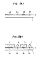
- the substrate shown in Fig. 1(A) is set in a thermal CVD apparatus, and the substrate temperature is raised to a given degree, followed by flowing a carrier gas and then a silicon source gas mixed in the carrier gas to cause Si crystals to grow.
- a substrate temperature of from 600°C to 1,200°C, particularly desirably from 800°C to 1,100°C.
- H2 gas and used as the silicon source gas are SiH4, SiH2Cl2, SiHCl3, SiCl4, SiF4, etc.
- HCl gas may also be optionally used as an additional gas.
- Si crystals grow only from the nucleation surfaces (S NDL ) 3A and 3B as shown in Fig. 1(B) and do not grow from the SiO2 film. Only the monocrystal is formed from the single nucleation surface (S NDL -S) 3A and a monocrystal 4 grows from this single nucleus until it covers the SiO2 film.
- the size of the single nucleation surface (S NDL -S) 3A is preferably 10 ⁇ m or smaller, more preferably 5 ⁇ m or smaller, optimally 1 ⁇ m or smaller.
- the grain size of the Si polycrystal in the multiple nucleation surface (S NDL -M) 3B at least depends on the nucleation density of the multiple nucleation surface (S NDL -M) 3B, where the larger the nucleation density is, the smaller the grain size becomes, or the smaller the nucleation density is, the grain size becomes larger.
- the size of a multiple-nucleation surface is desired to e large enough to allow as many nucleation as pollsible, and is preferably 20 ⁇ m or larger, more preferably 30 ⁇ m or larger.
- Fig. 2(A) is a view illustrating a cross-section of grown crystals
- Fig 2(B) a top plan view thereof.
- the technique presented by the present invention can achieve simultaneously the formation of Si monocrystals 4 and polycrystals 5 on any desired base substrate 1.
- the respective monocrystals and polycrystals can be formed in a controlled manner at any desired positions and in any desired shapes.
- the monocrystals and polycrystals thus formed are of sameness in the material and also can cover the whole surface of the substrate. Accordingly, the surface can be readily flattened. It is also readily possible to separate the respective monocrystals by the etching of grain boundaries of the respective monocrystals and to re-work the polycrystal areas into any desired shapes according to a photolithographic process.
- the grain boundaries of the above respective monocrystals can be formed at substantially the central position of a plurality of single nucleation surfaces (S NDL -S) 3A, thus making it possible to carry out the separation of the monocrystals at the grain boudary areas by the above etching, by using a photomask designed and prepared in advance.
- SiO2 film On an alumina substrate an SiO2 film was built up with a thickness of about 500 ⁇ by sputtering using Ar gas. Thereafter, a silicon nitride film was formed by using the reduced-pressure CVD process using SiH2Cl2 gas and NH3 gas as source gases at a substrate temperature of 800°C. Auger electron spectroscopy revealed that the Si/N ratio in the silicon nitride (Si x N y ) film was about 0.8.
- the above silicon nitride film was subjected to patterning by the photolithographic process to form four single nucleation surfaces (S NDL -S) 3A-1 to 3A-4 and one multiple nucleation surface (S NDL -M) 3B as shown in Fig. 4(A) and Fig. 4(B).
- the single nucleation surfaces had shapes of squares with a side of 1.0 ⁇ m each, and mutual distance thereof were 10 ⁇ m.
- the multiple nucleation surface (S NDL -M) was also made to have a shape of a rectangle of 20 ⁇ m long and 40 ⁇ m broad.
- a substrate temperature 1,030°C
- a gas flow rate of SiH2Cl2/HCl/H2 1.2 lit/min/1.5 lit/min/100 lit/min and a total pressure of 175 Torr.
- four monocrystals uniformly having a grain size of about 10 ⁇ m were found to have grown from the single nucleation surfaces (S NDL -S) 3A-1 to 3A-4, and the grain boundaries 6 were positioned substantially at the centers of the segments connecting the respective single nucleation surfaces.
- SiO x film On a fused quartz substrate the plasma CVD process was applied using SiH4 gas and oxygen gas, diluted with hydrogen gas, to form an SiO x film with a film thickness of about 1,000 ⁇ . Next, Si-ion implantation was effected only on desired positions on the above SiO x film with use of a focusing ion beam apparatus.
- the implantation was carried out under the conditions of an accelerated voltage of 50 keV, a beam diameter of 0.4 ⁇ m, and an implantation rate of 2 ⁇ 1018cm ⁇ 2 at the areas corresponding to the single nucleation surfaces (S NDL -S) 3A-5 to 3A-8, and 3 ⁇ 1019cm ⁇ 2 at the areas corresponding to the multiple nucleation surfaces (S NDL -M) 3B-5 to 3B-8.
- the single nucleation surfaces (S NDL -S) 3A-5 to 3A-8 were made to have shapes of squares with a side of 2.0 ⁇ m each, and the multiple nucleation surface (S NDL -M), shapes of rectangles of 20 ⁇ m long and 30 ⁇ m broad each.
- These single nucleation surfaces were each longwise arranged in a line with a distance of 25 ⁇ m between centers, and on the side area thereof the multiple nucleation surfaces were similarly longwise arranged in a line with a distance of 25 ⁇ m between centers.
- the distance between the center of a single nucleation surface and the center of a multiple nucleation surfaces were made to be 28 ⁇ m.
- a substrate temperature of 1,030°C 1,030°C
- a gas flow rate of SiH2Cl2/HCl/H2 1.7 lit/min/1.3 lit/min/100 lit/min
- a total pressure of 175 Torr As a result, there were obtained monocrystals 4-5 to 4-8 and polycrystals 5-5 to 5-8 as shown in the cross-section of Fig. 5(A) and the plan view of Fig. 5(C).
- the monocrystals 4 had a grain size of about 25 ⁇ m, and the polycrystals 5, an average grain size of about 0.5.
- the resulting crystals were flattened on these surfaces by mechanical grinding and chemical grinding to obtain a flat crystal thin film with average thickness of about 3 ⁇ m for both the monocrystals 4 and polycrystals 5.
- Fig. 6(B) On the flattened crystalline thin film (Fig. 5(B)) prepared in Example 2, a circuit as shown in Fig. 6(B) was prepared. Photodiodes were prepared on the monocrystalline areas 4, and switching MOS transistors, on the polycrystalline areas 5. A cross-section of the device at this time is shown in Fig. 6(A).
- the numeral 7 denotes the SiO2 film formed by the CVD process; 8 to 11, electrodes comprising transparent conductive films, wherein, 8, an electrode of the photodiode; 9, a source electrode of the MOS transistor; 10, a gate electrode; and 11, a drain electrode.
- the photodiodes were made to have shapes of squares with about 10 ⁇ m square each at the junction portion, and the MOS transistors, to have a channel length of 4 ⁇ m and a channel width of 6 ⁇ m for each.
- the MOS transistors had a field-effect mobility of about 3.0 cm2/V ⁇ s and a threshold voltage of about 3.5 V.
- pulses as shown in the timing chart of Fig.
Landscapes
- Chemical & Material Sciences (AREA)
- Chemical Kinetics & Catalysis (AREA)
- General Chemical & Material Sciences (AREA)
- Engineering & Computer Science (AREA)
- Crystallography & Structural Chemistry (AREA)
- Materials Engineering (AREA)
- Metallurgy (AREA)
- Organic Chemistry (AREA)
- Recrystallisation Techniques (AREA)
- Crystals, And After-Treatments Of Crystals (AREA)
Applications Claiming Priority (2)
| Application Number | Priority Date | Filing Date | Title |
|---|---|---|---|
| JP73516/87 | 1987-03-27 | ||
| JP62073516A JP2592834B2 (ja) | 1987-03-27 | 1987-03-27 | 結晶物品およびその形成方法 |
Publications (3)
| Publication Number | Publication Date |
|---|---|
| EP0284433A2 true EP0284433A2 (de) | 1988-09-28 |
| EP0284433A3 EP0284433A3 (de) | 1989-03-08 |
| EP0284433B1 EP0284433B1 (de) | 1998-12-02 |
Family
ID=13520487
Family Applications (1)
| Application Number | Title | Priority Date | Filing Date |
|---|---|---|---|
| EP88302717A Expired - Lifetime EP0284433B1 (de) | 1987-03-27 | 1988-03-25 | Kristalline Gegenstände und Verfahren zu ihrer Herstellung |
Country Status (4)
| Country | Link |
|---|---|
| EP (1) | EP0284433B1 (de) |
| JP (1) | JP2592834B2 (de) |
| CA (1) | CA1339827C (de) |
| DE (1) | DE3856275T2 (de) |
Cited By (3)
| Publication number | Priority date | Publication date | Assignee | Title |
|---|---|---|---|---|
| EP0364139A1 (de) * | 1988-10-02 | 1990-04-18 | Canon Kabushiki Kaisha | Gegenstand aus Kristall und Verfahren zu seiner Herstellung |
| EP0510587A1 (de) * | 1991-04-22 | 1992-10-28 | Canon Kabushiki Kaisha | Lichtemittierende Vorrichtung unter Verwendung von polykristallinem Halbleitermaterial und Herstellungsverfahren dafür |
| EP0514889A1 (de) * | 1991-05-23 | 1992-11-25 | Canon Kabushiki Kaisha | Lichtemittierende Vorrichtung, optischer Druckkopf mit solcher Vorrichtung, und optischer Drucker mit solchem Druckkopf |
Family Cites Families (4)
| Publication number | Priority date | Publication date | Assignee | Title |
|---|---|---|---|---|
| US3620833A (en) * | 1966-12-23 | 1971-11-16 | Texas Instruments Inc | Integrated circuit fabrication |
| JPS6046074B2 (ja) * | 1981-06-30 | 1985-10-14 | 日本電信電話株式会社 | 半導体結晶成長方法 |
| US4657603A (en) * | 1984-10-10 | 1987-04-14 | Siemens Aktiengesellschaft | Method for the manufacture of gallium arsenide thin film solar cells |
| JPH0782996B2 (ja) * | 1986-03-28 | 1995-09-06 | キヤノン株式会社 | 結晶の形成方法 |
-
1987
- 1987-03-27 JP JP62073516A patent/JP2592834B2/ja not_active Expired - Fee Related
-
1988
- 1988-03-25 DE DE3856275T patent/DE3856275T2/de not_active Expired - Fee Related
- 1988-03-25 EP EP88302717A patent/EP0284433B1/de not_active Expired - Lifetime
- 1988-03-25 CA CA000562511A patent/CA1339827C/en not_active Expired - Fee Related
Cited By (5)
| Publication number | Priority date | Publication date | Assignee | Title |
|---|---|---|---|---|
| EP0364139A1 (de) * | 1988-10-02 | 1990-04-18 | Canon Kabushiki Kaisha | Gegenstand aus Kristall und Verfahren zu seiner Herstellung |
| US5320907A (en) * | 1988-10-02 | 1994-06-14 | Canon Kabushiki Kaisha | Crystal article and method for forming same |
| EP0510587A1 (de) * | 1991-04-22 | 1992-10-28 | Canon Kabushiki Kaisha | Lichtemittierende Vorrichtung unter Verwendung von polykristallinem Halbleitermaterial und Herstellungsverfahren dafür |
| US5369290A (en) * | 1991-04-22 | 1994-11-29 | Canon Kabushiki Kaisha | Light emission element using a polycrystalline semiconductor material of III-V group compound |
| EP0514889A1 (de) * | 1991-05-23 | 1992-11-25 | Canon Kabushiki Kaisha | Lichtemittierende Vorrichtung, optischer Druckkopf mit solcher Vorrichtung, und optischer Drucker mit solchem Druckkopf |
Also Published As
| Publication number | Publication date |
|---|---|
| CA1339827C (en) | 1998-04-21 |
| DE3856275D1 (de) | 1999-01-14 |
| JP2592834B2 (ja) | 1997-03-19 |
| JPS63239186A (ja) | 1988-10-05 |
| EP0284433A3 (de) | 1989-03-08 |
| EP0284433B1 (de) | 1998-12-02 |
| DE3856275T2 (de) | 1999-05-12 |
Similar Documents
| Publication | Publication Date | Title |
|---|---|---|
| US5733369A (en) | Method for forming crystal | |
| US5281283A (en) | Group III-V compound crystal article using selective epitaxial growth | |
| US5130103A (en) | Method for forming semiconductor crystal and semiconductor crystal article obtained by said method | |
| US5846320A (en) | Method for forming crystal and crystal article obtained by said method | |
| US5447117A (en) | Crystal article, method for producing the same and semiconductor device utilizing the same | |
| JP2596547B2 (ja) | 太陽電池及びその製造方法 | |
| JPH06140346A (ja) | ヘテロエピタキシアルの薄い層と電子デバイスの製造法 | |
| EP0240309B1 (de) | Herstellungsverfahren eines Kristalls und so hergestellter Kristall | |
| EP0241204B1 (de) | Herstellungsverfahren einer niedergeschlagenen Kristallschicht | |
| US5364815A (en) | Crystal articles and method for forming the same | |
| AU631117B2 (en) | Method for forming crystal | |
| CA1339827C (en) | Crystal articles and method for forming the same | |
| AU651806B2 (en) | Method for forming crystalline deposited film | |
| US5190613A (en) | Method for forming crystals | |
| US5118365A (en) | Ii-iv group compound crystal article and process for producing same | |
| CA1333248C (en) | Method of forming crystals | |
| EP0284435B1 (de) | Selektives Herstellungsverfahren von Schichten aus II-VI-Verbindungen | |
| US5254211A (en) | Method for forming crystals | |
| EP0284437A2 (de) | Kristalliner Gegenstand aus III-V-Gruppe-Verbindung und Verfahren zu seiner Herstellung | |
| JP2659745B2 (ja) | ▲iii▼−v族化合物結晶物品およびその形成方法 | |
| JP2659746B2 (ja) | ▲ii▼−▲vi▼族化合物結晶物品およびその形成方法 | |
| US5463975A (en) | Process for producing crystal | |
| EP0455981A1 (de) | Verfahren zur Herstellung von Kristallen | |
| JPH04130717A (ja) | 結晶の形成方法 | |
| JP2592832B2 (ja) | 結晶の形成方法 |
Legal Events
| Date | Code | Title | Description |
|---|---|---|---|
| PUAI | Public reference made under article 153(3) epc to a published international application that has entered the european phase |
Free format text: ORIGINAL CODE: 0009012 |
|
| AK | Designated contracting states |
Kind code of ref document: A2 Designated state(s): DE FR GB IT NL |
|
| PUAL | Search report despatched |
Free format text: ORIGINAL CODE: 0009013 |
|
| RHK1 | Main classification (correction) |
Ipc: H01L 21/20 |
|
| AK | Designated contracting states |
Kind code of ref document: A3 Designated state(s): DE FR GB IT NL |
|
| 17P | Request for examination filed |
Effective date: 19890726 |
|
| 17Q | First examination report despatched |
Effective date: 19910718 |
|
| GRAG | Despatch of communication of intention to grant |
Free format text: ORIGINAL CODE: EPIDOS AGRA |
|
| GRAG | Despatch of communication of intention to grant |
Free format text: ORIGINAL CODE: EPIDOS AGRA |
|
| GRAH | Despatch of communication of intention to grant a patent |
Free format text: ORIGINAL CODE: EPIDOS IGRA |
|
| GRAH | Despatch of communication of intention to grant a patent |
Free format text: ORIGINAL CODE: EPIDOS IGRA |
|
| GRAA | (expected) grant |
Free format text: ORIGINAL CODE: 0009210 |
|
| AK | Designated contracting states |
Kind code of ref document: B1 Designated state(s): DE FR GB IT NL |
|
| PG25 | Lapsed in a contracting state [announced via postgrant information from national office to epo] |
Ref country code: IT Free format text: LAPSE BECAUSE OF FAILURE TO SUBMIT A TRANSLATION OF THE DESCRIPTION OR TO PAY THE FEE WITHIN THE PRE;WARNING: LAPSES OF ITALIAN PATENTS WITH EFFECTIVE DATE BEFORE 2007 MAY HAVE OCCURRED AT ANY TIME BEFORE 2007. THE CORRECT EFFECTIVE DATE MAY BE DIFFERENT FROM THE ONE RECORDED.SCRIBED TIME-LIMIT Effective date: 19981202 Ref country code: NL Free format text: LAPSE BECAUSE OF FAILURE TO SUBMIT A TRANSLATION OF THE DESCRIPTION OR TO PAY THE FEE WITHIN THE PRESCRIBED TIME-LIMIT Effective date: 19981202 |
|
| REF | Corresponds to: |
Ref document number: 3856275 Country of ref document: DE Date of ref document: 19990114 |
|
| ET | Fr: translation filed | ||
| NLV1 | Nl: lapsed or annulled due to failure to fulfill the requirements of art. 29p and 29m of the patents act | ||
| PLBE | No opposition filed within time limit |
Free format text: ORIGINAL CODE: 0009261 |
|
| STAA | Information on the status of an ep patent application or granted ep patent |
Free format text: STATUS: NO OPPOSITION FILED WITHIN TIME LIMIT |
|
| 26N | No opposition filed | ||
| REG | Reference to a national code |
Ref country code: GB Ref legal event code: IF02 |
|
| PGFP | Annual fee paid to national office [announced via postgrant information from national office to epo] |
Ref country code: GB Payment date: 20030311 Year of fee payment: 16 |
|
| PGFP | Annual fee paid to national office [announced via postgrant information from national office to epo] |
Ref country code: FR Payment date: 20030321 Year of fee payment: 16 |
|
| PGFP | Annual fee paid to national office [announced via postgrant information from national office to epo] |
Ref country code: DE Payment date: 20030327 Year of fee payment: 16 |
|
| PG25 | Lapsed in a contracting state [announced via postgrant information from national office to epo] |
Ref country code: GB Free format text: LAPSE BECAUSE OF NON-PAYMENT OF DUE FEES Effective date: 20040325 |
|
| PG25 | Lapsed in a contracting state [announced via postgrant information from national office to epo] |
Ref country code: DE Free format text: LAPSE BECAUSE OF NON-PAYMENT OF DUE FEES Effective date: 20041001 |
|
| GBPC | Gb: european patent ceased through non-payment of renewal fee |
Effective date: 20040325 |
|
| PG25 | Lapsed in a contracting state [announced via postgrant information from national office to epo] |
Ref country code: FR Free format text: LAPSE BECAUSE OF NON-PAYMENT OF DUE FEES Effective date: 20041130 |
|
| REG | Reference to a national code |
Ref country code: FR Ref legal event code: ST |