EP0455981A1 - Verfahren zur Herstellung von Kristallen - Google Patents
Verfahren zur Herstellung von Kristallen Download PDFInfo
- Publication number
- EP0455981A1 EP0455981A1 EP91105269A EP91105269A EP0455981A1 EP 0455981 A1 EP0455981 A1 EP 0455981A1 EP 91105269 A EP91105269 A EP 91105269A EP 91105269 A EP91105269 A EP 91105269A EP 0455981 A1 EP0455981 A1 EP 0455981A1
- Authority
- EP
- European Patent Office
- Prior art keywords
- nucleation
- crystal
- substrate
- nucleation surface
- forming
- Prior art date
- Legal status (The legal status is an assumption and is not a legal conclusion. Google has not performed a legal analysis and makes no representation as to the accuracy of the status listed.)
- Ceased
Links
Images


Classifications
-
- C—CHEMISTRY; METALLURGY
- C30—CRYSTAL GROWTH
- C30B—SINGLE-CRYSTAL GROWTH; UNIDIRECTIONAL SOLIDIFICATION OF EUTECTIC MATERIAL OR UNIDIRECTIONAL DEMIXING OF EUTECTOID MATERIAL; REFINING BY ZONE-MELTING OF MATERIAL; PRODUCTION OF A HOMOGENEOUS POLYCRYSTALLINE MATERIAL WITH DEFINED STRUCTURE; SINGLE CRYSTALS OR HOMOGENEOUS POLYCRYSTALLINE MATERIAL WITH DEFINED STRUCTURE; AFTER-TREATMENT OF SINGLE CRYSTALS OR A HOMOGENEOUS POLYCRYSTALLINE MATERIAL WITH DEFINED STRUCTURE; APPARATUS THEREFOR
- C30B25/00—Single-crystal growth by chemical reaction of reactive gases, e.g. chemical vapour-deposition growth
- C30B25/02—Epitaxial-layer growth
- C30B25/18—Epitaxial-layer growth characterised by the substrate
-
- H—ELECTRICITY
- H01—ELECTRIC ELEMENTS
- H01L—SEMICONDUCTOR DEVICES NOT COVERED BY CLASS H10
- H01L21/00—Processes or apparatus adapted for the manufacture or treatment of semiconductor or solid state devices or of parts thereof
- H01L21/02—Manufacture or treatment of semiconductor devices or of parts thereof
- H01L21/02104—Forming layers
- H01L21/02365—Forming inorganic semiconducting materials on a substrate
- H01L21/02367—Substrates
- H01L21/0237—Materials
- H01L21/02373—Group 14 semiconducting materials
- H01L21/02381—Silicon, silicon germanium, germanium
-
- H—ELECTRICITY
- H01—ELECTRIC ELEMENTS
- H01L—SEMICONDUCTOR DEVICES NOT COVERED BY CLASS H10
- H01L21/00—Processes or apparatus adapted for the manufacture or treatment of semiconductor or solid state devices or of parts thereof
- H01L21/02—Manufacture or treatment of semiconductor devices or of parts thereof
- H01L21/02104—Forming layers
- H01L21/02365—Forming inorganic semiconducting materials on a substrate
- H01L21/02612—Formation types
- H01L21/02617—Deposition types
- H01L21/0262—Reduction or decomposition of gaseous compounds, e.g. CVD
-
- H—ELECTRICITY
- H01—ELECTRIC ELEMENTS
- H01L—SEMICONDUCTOR DEVICES NOT COVERED BY CLASS H10
- H01L21/00—Processes or apparatus adapted for the manufacture or treatment of semiconductor or solid state devices or of parts thereof
- H01L21/02—Manufacture or treatment of semiconductor devices or of parts thereof
- H01L21/02104—Forming layers
- H01L21/02365—Forming inorganic semiconducting materials on a substrate
- H01L21/02612—Formation types
- H01L21/02617—Deposition types
- H01L21/02636—Selective deposition, e.g. simultaneous growth of mono- and non-monocrystalline semiconductor materials
- H01L21/02639—Preparation of substrate for selective deposition
- H01L21/02645—Seed materials
Definitions
- the present invention relates to a method of forming a crystal, particularly to a crystal forming method for growing a single-crystal by subjecting a substrate having a free surface on which a non-nucleation surface and a nucleation surface are arranged adjacent to each other to a crystal forming process.
- the nucleation surface has a greater nucleation density than the non-nucleation surface with respect to a material with which the single-crystal will be formed.
- the nucleation surface has an area sufficiently small to selectively permit only one nucleus to form, which will grow to form a single-crystal.
- the method of the present invention forms a crystal which is used, for example, as an electronic, optical, magnetic, piezoelectric or surface acoustic element of a semiconductor integrated circuit, an optical integrated circuit, or a magnetic circuit.
- single crystal thin films to be used for semiconductor electronic devices or optical devices have been formed by epitaxial growth on a single crystal substrate.
- epitaxial growth of Si, Ge, GaAs, etc. can be performed from the liquid phase, gas phase or solid phase on Si single crystal substrate (silicon wafer), and it is also known that epitaxial growth of a single crystal such as GaAs, GaAlAs, etc., occurs on a GaAs single crystal substrate.
- semiconductor devices and integrated circuits, electroluminescent devices such as semiconductor lasers or LED have been prepared.
- the method for forming a single crystal thin film of the prior art by epitaxial growth may be understood to be dependent greatly on its substrate material.
- Mathews et al. have examined combinations of the substrate material with epitaxial growth layer (EPITAXIAL GROWTH, Academic Press, New York, 1975, ed. by J.W. Mathews).
- the growth of a crystalline silicon on a crystalline silicon substrate is essentially two-dimensional growth, which is formed layer-by-layer by atomic arrangement on the lattice of the single crystal substrate.
- the presence of matching lattice constants and matching coefficients of thermal expansion between the single crystal material and the epitaxial growth layer make possible the formation of a uniform single crystal.
- the order in the single crystal substrate is carried over and matched during epitaxial growth.
- overlayers are amorphous overlayers, or, at best, polycrystalline overlayers, which are aggregates of small random-sized crystal grains with grain boundaries between adjacent grains.
- Both silicon oxides and silicon nitrides are stable amorphous materials, which have been widely used for silicon integrated circuit processing. Such amorphous compounds are formed by chemical vapor deposition.
- silicon was deposited on amorphous silicon oxide, or amorphous silicon nitride, an amorphous layer or at best, a polycrystalline silicon layer, was formed with a variety of grain sizes. That is because the silicon layer was formed by spontaneous nucleation, coalescence and recrystallization. In that disordered system, the crystal grain boundary locations were randomly determined, since the silicon nuclei were randomly formed over the substrate surface. Closely located nuclei formed small grains, while more remote nuclei formed larger grains due to the difference in time before interaction with adjacent grains.
- the size of the substrate is presently about 6 inches for a Si wafer, and the enlargement of GaAs and sapphire substrate is further inhibited.
- the single crystal substrate is high in production cost, the cost per chip becomes higher.
- the crystal structure of the deposited film becomes amorphous or polycrystalline.
- the amorphous film refers to a state in which near distance order to the extent of the closest atoms is preserved, but no longer distance order exists, while the polycrystalline film refers to single crystal grains having no specific crystal direction gathered as separated at the grain boundaries.
- the deposition temperature is abut 600°C or lower, it becomes an amorphous silicon, while it becomes a polycrystalline silicon with grain sizes distributed between some hundred to some thousand ⁇ at a temperature higher than said temperature.
- the grain sizes and their distribution of polycrystalline silicon will be varied greatly depending on the formation method.
- Diamond thin film which is particularly broad in bandgap as 5.5 eV as the semiconductor, can be actuated at higher temperature (about 500°C or less) as compared with Si, Ge, GaAs, etc., which are semiconductor materials of the prior art. Also, the carrier mobility of both electrons and positive holes surpass that of Si (1800 cm2/V ⁇ sec from electrons, 1600 cm2/V ⁇ sec for positive holes), and thermal conductivity is also extremely high. For this reason, it has been expected to be promising for application in semiconductor devices of the great consumption power type with great heat generation quantity.
- diamond nuclei are generated by utilizing excitation with microwaves, using a hydrocarbon type gas such as CH4, etc., and by irradiation with a hot filament or an electron beam, but the nucleation density is generally low, whereby a continuous thin film can only be obtained with difficulty. Even if a continuous thin film may be formed, it has a polycrystalline structure with great grain size distribution and is difficult to apply for semiconductor devices.
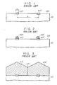
- a substrate 401 having a surface 403 with a small nucleation density is prepared, and regions 407 and 407' with a diameter a and with a nucleation density greater than that of the surface 403 are arranged on the substrate 401 at a pitch of b .
- the substrate 401 is subjected to a predetermined crystal forming process, whereby nuclei 409 and 409' made of a deposited substance (the substance with which the crystals are to be formed) are generated only on the surfaces of the regions 407 and 407', respectively, whereas no nuclei are generated on the surface 403.
- nucleation surfaces surfaces corresponding to the surfaces of the regions 407 and 407' will be referred to as “nucleation surfaces”
- those corresponding to the surface 403 will be referred to as “non-nucleation surfaces”.
- the nuclei 409 and 409' generated on the nucleation surfaces of the regions 407 and 407', respectively, are grown so that they grow beyond the nucleation surface regions 407 and 407' until, finally, the crystal grain 410 grown from the nucleation surface 407 abuts on the crystal grain 410' grown from the adjacent nucleation surface 407' to define a grain boundary 411.
- the first report described an example in which amorphous Si3N4 was the material used to form a plurality of nucleation surfaces arranged at desired positions on the substrate, while SiO2 was the material used to form the non-nucleation surfaces.
- a Si single-crystal was formed on each nucleation surface by a chemical vapor deposition (CVD) method.
- the crystal forming method as described in the first report entails the following problems concerning control over the crystal formation. This is because under certain crystal growth conditions, the difference in nucleation density between Si3N4 and SiO2 is insufficient, corresponding to a ratio of about 1000 : 1 at most.
- nucleation surfaces and the non-nucleation surfaces may not have any nuclei generated thereon to grow into single-crystals. Hence, these surfaces may not be able to grow single-crystals.
- the nucleation densities are determined based on a one-to-one relationship under the given crystal growth conditions. For this reason, it is sometimes difficult to determine, under certain crystal growth conditions adapted to avoid unnecessary nucleation on the non-nucleation surfaces, a particular nucleation density on the nucleation surfaces which assures that a crystal grown from a single nucleus is formed on each of the nucleation surfaces. It is also difficult to suppress, under certain crystal growth conditions adapted to assure that a nucleus is generated and grows into a single-crystal, unnecessary generation of nuclei and unnecessary growth of crystals on the non-nucleation surfaces. Thus, under certain crystal growth conditions, it is difficult to fill a large area with good-quality crystal grains, in which grain size and the grain boundary positions are successfully controlled. As a result, it is difficult to improve the yield of the crystals.
- the second method used nucleation surfaces consisting of regions where the nucleation density is increased by ion implantation employing a focused ion beam.
- nucleation surfaces are formed in the following manner: a mask of a photoresist is patterned by a resist process so that it has openings only at positions corresponding to the regions where ions should be implanted; then, ion implantation is performed throughout the surface of a substrate over the mask, thereby implanting ions only in those portions of the substrate surface which are to serve as the nucleation surfaces.
- ion implantation is performed at a high dose, the photoresist may have its properties changed in the vicinity of the openings, thereby making stripping of the photoresist difficult.
- the present invention solves the problem of forming crystals over non-monocrystalline substrate surfaces.
- two growth factors must be controlled.
- the crystal growth must grow on a nucleation surface of (1) sufficiently small area and (2) of sufficient nucleation density to selectively grow only a single nucleus.
- the single nucleus grows to form a crystal. By patterning the nucleation surface, large grains of single crystals can be formed having well-defined and uniform grain boundaries.
- an object of the present invention is to provide a method of forming crystals in which the difference in nucleation density between the nucleation surfaces and the non-nucleation surfaces of a substrate is sufficient to generate a nucleus on each nucleation surface, thereby improving the yield of the selective growth of crystals.
- Another object of the present invention is to provide a method of forming crystals in which an ion implantation process is performed without employing a resist.
- this method there is no generation of denaturant or other unwanted substances even when a large dosage of ions are implanted.
- a further object of the present invention is to provide a method of forming crystals in which selective etching is performed without using a resist. Instead, the method utilizes the difference in the etching rate between the material forming the nucleation surfaces and the material forming the non-nucleation surfaces, thus simplifying the entire process.
- a method of forming a single-crystal on a substrate comprising: (a) providing a substrate having a non-nucleation surface and a nucleation surface made of an amorphous material arranged adjacent to each other wherein the nucleation surface has a sufficiently greater nucleation density than the non-nucleation surface to selectively form a single nucleus, the nucleation surface has an area sufficiently small, that is, an area 10 ⁇ m or less in maximum diameter, to permit only one nucleus to form, which will grow into a single crystal, and the non-nucleation surface is composed of a material having a greater etching rate than the material of which the nucleation surface is composed; (b) implanting ions in the substrate; (c) selectively etching the substrate implanted with the ions such that only the non-nucleation surface is etched; and (d) growing by vapor deposition a single crystal from a single nucleus formed on the nucleation surface and
- nucleation density is used to mean the number of nuclei generated per unit area.
- nuclei means the following: When the substrate surface (the deposition surface) is made of a material different from the atoms being projected, particularly when the surface is made of an amorphous material, the atoms projected freely diffuse over the surface of the substrate, or diffuse and re-evaporate (i.e., are desorbed). As a result of atoms colliding with each other, aggregates of atoms are formed.
- ⁇ 0 the surface energy between each aggregate and vacuum
- g v the free energy per unit volume
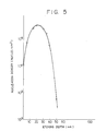
- the free energy G changes with changes in the size (the radius of curvature) of the aggregate or nucleus in the manner shown in Fig. 4. As shown in this graph, when the the radius of curvature is equal to r c , the free energy G is at the extremum (maximum: G max ).
- a method of forming crystals according to the present invention provides nucleation surface forming regions made of a nucleation surface material and non-nucleation surface forming regions made of a non-nucleation surface material having a higher etching rate than the nucleation surface material, the two different regions are positioned adjacent to each other, and ions are implanted in the nucleation surface forming regions and the non-nucleation surface forming regions. This is followed by the selective etching of the ion-implanted portions of the non-nucleation surface forming regions.
- the method according to the present invention is capable of increasing the difference in nucleation density between the nucleation and non-nucleation surfaces, and is hence capable of increasing the yield of crystal formation.
- the nucleation density reaches the extremum (the maximum) when the etching depth corresponds to the projection range.
- the nucleation density at such a depth is lower than the nucleation density on the surface.
- the removal of those affected areas in the non-nucleation surface material resulting from the ion implantation is performed by selective etching without employing a resist. Instead, their removal is achieved by utilizing the difference in the etching rate.
- This feature is advantageous in that it is possible to completely avoid the problem of changes in the properties of the resist, conventionally caused by ion implantation.
- Another advantage is that, since selective etching is performed, there is no need to prepare a newly patterned resist for the etching process. Therefore, the difficult operation of removing the resist becomes unnecessary and can be accomplished without increasing the number of processes required. This method thereby improves the level of control over the generation of nuclei.
- nucleation surfaces and non-nucleation surfaces are arranged on a substrate.
- a part of the substrate is made of a base material 101 which may be of any type and may have any shape so long as it is suitable for a crystal forming process.
- Preferable examples include a Si wafer, quartz (silica), high-melting-point glass, and metals.
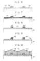
- nucleation surface forming region 104 and non-nucleation surface forming region 105 are formed on the base material 101 by ion implantation, as shown in Fig. 6, thereby preparing a substrate having two kinds of regions 104 and 105.
- the nucleation surface material is an amorphous material having an etching rate slower than that of the non-nucleation surface material. This is because it is desired that the nucleation surface forming regions 104 remain substantially unetched even when the non-nucleation surface forming region 105 is etched to remove the upper portion 112 (the ion implanted portion) where there is a high concentration of ions unnecessarily implanted in the region 105 (see Figs. 7 and 8).
- the portions of the region 104 with a high concentration of implanted ions can be maintained. This allows the nucleation surface to have a nucleation density which is at least 1000 times higher than that of the non-nucleation surface
- the method according to the present invention is particularly advantageous in that it is able to achieve a nucleation density of the nucleation surface material which is at least 103 times the nucleation density of the non-nucleation surface material, thereby enabling crystal growth to take place with good selectivity.
- the nucleation surface preferably has a maximum diameter of not greater than 10 ⁇ m, more preferably, a maximum diameter of 0.1 ⁇ m to 5 ⁇ m. That is, the nucleation surface must be of sufficiently small area and of sufficient nucleation density to selectively grow a single nucleus only.
- the nucleation surface material may be, for example, silicon nitride when the non-nucleation surface material is silicon oxide.
- the nucleation surface is formed by implanting ions in the nucleation surface forming region 104.
- the ion species implanted is preferably the same element or common element that will form the crystals to be grown. For instance, if silicon crystal is to be grown, silicon ions are implanted. However, ions that can be implanted are not limited to ions of the element that will form the crystal to be grown. Any ion species can be implanted so long as the nucleation density of the nucleation surfaces is increased by ion implantation.
- the non-nucleation surface material is a material which assures a lower nucleation density of the non-nucleation surface than that of the nucleation surface, and which has a higher etching rate than the nucleation surface material.
- the non-nucleation surface material is silicon oxide.
- ion implantation is performed over the entire surface of the substrate, on which are arranged the non-nucleation surface of the region 105 and the nucleation surface of the region 104.
- Region 104 has an area sufficiently small to permit only one nucleus to be generated. This single nucleus will, in a crystal forming process, grow into a single-crystal.
- Ions are implanted in both portions 112 and 112' of the regions 105 and 104.
- the ion implantation conditions such as the acceleration voltage and the dose, are so determined as to assure a sufficiently great nucleation density of the nucleation surfaces in the portions 112'.
- the ion implantation should be performed at a low acceleration voltage so that the ion species concentration is generally high in the vicinity of the surface.
- the dose is at least 1016 ions/cm2 when nuclei for the formation of, e.g., Si crystal, are to be generated on the nucleation surface.
- the acceleration voltage for the ion implantation should not exceed an allowable upper limit, which is preferably 50 keV, and more preferably 30 keV, from the view point of curtailing the time required for the etching process and improving the selectivity of the crystal formation.
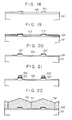
- An example of this relationship is shown in Fig. 11. Specifically, when silicon ions were implanted in silicon oxide sample, and when the excessive Si atom concentration on the sample surfaces was determined, the results showed that the relationship of that excessive Si concentration with the nucleation density was represented by a characteristic curve such as that shown in the graph (Fig. 11).
- Ion implantation (shown in Fig. 7) causes an increase in the nucleation density of the ion-implanted portions 112 as well as in the non-nucleation surface forming regions 105. This is because the concentration of the implanted ion species increases also in the non-nucleation surface forming regions 105.
- the ion species implanted by ion implantation are distributed at various depths of the material in the manner shown in Fig. 12.
- the concentration of the implanted ion species has a distribution approximating Gaussian distribution, that is, a distribution which is determined by the type of implanted ion species, the material implanted, and the acceleration voltage, and which is centered on the depth corresponding to the projection range (i.e., the depth at which the concentration of the implanted ions is the maximum).
- the non-nucleation surface forming regions 105 are selectively etched, with an etchant such as a hydrogen fluoride (HF) aqueous solution or an HF gas, to a certain depth where the concentration of the implanted ion species is low enough to avoid influencing the nucleation density.
- a hydrogen fluoride (HF) aqueous solution or an HF gas such as a hydrogen fluoride (HF) aqueous solution or an HF gas
- the projection range and the standard deviation of the distribution pattern of the implanted ion species are approximately determined by the implanted ion species, the surface implanted, and the implantation energy. It is desired that the depth to which the regions 105 are etched be great enough to achieve a lower concentration of the implanted ion species on the exposed surfaces than that of the unetched surfaces. For this purpose, it is desired that the etching be performed to a depth preferably corresponding to two times the projection range, and preferably more than two times the projection range. Specifically, the etching should be performed to a depth at least equal to a value which is preferably the sum of the projection range and three times the standard deviation, and preferably, the sum of the projection range and five times the standard deviation.
- the etching be performed to a depth which assures that the ion species (Si) concentration on the exposed non-nucleation surfaces 103 will preferably be not more than 5 x 1013 cm ⁇ 2, and more preferably be not more than 2 x 1013 cm ⁇ 2. If the difference in the etching rates selected is not sufficient, the nucleation surface material may be etched.
- the preferred ratio is 1000 : 1, preferably, 104 : 1.
- the etching method adopted may be any of the following methods: wet process etching employing an acid or alkali solution; dry process etching employing an etching gas such as halogenated hydrogen gas; and a reactive ion etching (RIE) method employing plasma.
- the nucleation surface material is silicon nitride and the non-nucleation surface material is silicon oxide
- hydrofluoric acid or the like is used.
- the etching rate of silicon oxide with respect to buffered hydrofluoric acid is about 500 ⁇ /min., whereas that of silicon nitride is about 0 ⁇ /min., rendering silicon nitride substantially unetched.
- the resultant substrate is then subjected to a crystal forming process.
- the crystal forming process should desirably be a physical vapor deposition (PVD) method such as evaporation or sputtering, or a chemical vapor deposition (CVD) method such as thermal CVD, metal organic CVD (MOCVD), or plasma CVD.
- PVD physical vapor deposition
- CVD chemical vapor deposition
- the crystal forming process employing such a method generates nuclei 109 and 109' on the nucleation surfaces 107 and 107', respectively, which will grow into single-crystals.
- the nuclei are grown, thereby forming single-crystals 110 and 110' which have grown, starting at the nucleation surfaces 107 and 107', until they abut on each other to define a crystal grain boundary 111.
- Example 1 a plurality of Si single-crystals were formed by the method according to the present invention in the following manner.
- the crystal growth by vapor deposition was continued whereby silicon a single-crystal 110 and a silicon single-crystal 110' each having a size of 40 ⁇ m were grown, respectively, from single nucleus 109 and single nucleus 109'.
- the growth began starting at the adjacent nucleation surfaces 107 and 107', respectively, until the single-crystals abutted on one another, as shown in Fig. 17.
- the grown crystals 110 and 110' defined a grain boundary 111 at a substantially intermediate position between the nucleation surfaces 107 and 107'.
- An examination was made to determine whether any error crystals were formed by unnecessary generation of, and growth of, nuclei on the non-nucleation surfaces 103 and no formation of such error cyrstals was observed. Nor was there any observation of the formation of poly-crystalline error crystals on the nucleation surfaces where single-crystals should be formed.
- Example 1 single-crystals were formed with good selectivity, and having a grain size and a grain boundary position which were both successfully controlled.
- Example 2 a plurality of Si single-crystals were formed in the following manner.
- the method of forming crystals according to the present invention is capable of increasing the nucleation density of the nucleation surfaces by implanting ions in the substrate surface without employing resist. Further, since the affected layers (unnecessarily ion-implanted portions) resulting in the non-nucleation surface forming regions from ion implantation can be removed by a selective etching, whereby only the non-nucleation surface material is effected. These features make it possible to achieve a sufficiently great difference between the respective nucleation densities of the nucleation and non-nucleation surfaces.
- the ion implantation process that does not employ a resist renders the method completely free from the problems conventionally caused by ion-implantation using a resist, such as a lowered level of selectivity of the crystal growth.
- the selective etching which utilizes the difference between the respective etching rates of the nucleation and non-nucleation surface materials does not require the process of patterning a resist.
- a method of forming crystals is adapted to grow a single-crystal by subjecting a substrate having a free surface with mutually adjacent non-nucleation and nucleation surfaces to a crystal forming process.
- Each nucleation surface consists of an amorphous material, having a greater nucleation density than the non-nucleation surface, with respect to a material with which the single-crystal will be formed, and having an area sufficiently small to permit only one nucleus to be generated, which will grow into the single crystal.
- the non-nucleation surfaces are made of a material having a higher etching rate than the material of which the nucleation surfaces are made.
- the resultant substrate is subjected to an etching process whereby the non-nucleation surface material alone is selectively etched to remove the unnecessarily ion-implanted portions of the material.
Applications Claiming Priority (4)
| Application Number | Priority Date | Filing Date | Title |
|---|---|---|---|
| JP9044290 | 1990-04-06 | ||
| JP90442/90 | 1990-04-06 | ||
| JP89118/91 | 1991-03-29 | ||
| JP8911891A JP2825676B2 (ja) | 1990-04-06 | 1991-03-29 | 結晶の形成方法 |
Publications (1)
| Publication Number | Publication Date |
|---|---|
| EP0455981A1 true EP0455981A1 (de) | 1991-11-13 |
Family
ID=26430550
Family Applications (1)
| Application Number | Title | Priority Date | Filing Date |
|---|---|---|---|
| EP91105269A Ceased EP0455981A1 (de) | 1990-04-06 | 1991-04-03 | Verfahren zur Herstellung von Kristallen |
Country Status (2)
| Country | Link |
|---|---|
| EP (1) | EP0455981A1 (de) |
| JP (1) | JP2825676B2 (de) |
Cited By (2)
| Publication number | Priority date | Publication date | Assignee | Title |
|---|---|---|---|---|
| EP0412755A1 (de) * | 1989-08-07 | 1991-02-13 | Canon Kabushiki Kaisha | Verfahren zur Herstellung eines kristallinen Halbleiterfilms |
| WO2000017932A1 (de) * | 1998-09-21 | 2000-03-30 | Institut für Halbleiterphysik Frankfurt (Oder) GmbH | Bipolartransistor und verfahren zu seiner herstellung |
Families Citing this family (1)
| Publication number | Priority date | Publication date | Assignee | Title |
|---|---|---|---|---|
| US5792270A (en) * | 1993-10-21 | 1998-08-11 | Saxena; Arjun | Apparatus for forming a pattern of nucleation sites |
Citations (2)
| Publication number | Priority date | Publication date | Assignee | Title |
|---|---|---|---|---|
| EP0307108A1 (de) * | 1987-08-24 | 1989-03-15 | Canon Kabushiki Kaisha | Verfahren zur Herstellung von Kristallen |
| EP0339793A1 (de) * | 1988-03-27 | 1989-11-02 | Canon Kabushiki Kaisha | Verfahren zur Herstellung einer Kristallschicht auf einem Substrat |
-
1991
- 1991-03-29 JP JP8911891A patent/JP2825676B2/ja not_active Expired - Fee Related
- 1991-04-03 EP EP91105269A patent/EP0455981A1/de not_active Ceased
Patent Citations (2)
| Publication number | Priority date | Publication date | Assignee | Title |
|---|---|---|---|---|
| EP0307108A1 (de) * | 1987-08-24 | 1989-03-15 | Canon Kabushiki Kaisha | Verfahren zur Herstellung von Kristallen |
| EP0339793A1 (de) * | 1988-03-27 | 1989-11-02 | Canon Kabushiki Kaisha | Verfahren zur Herstellung einer Kristallschicht auf einem Substrat |
Cited By (2)
| Publication number | Priority date | Publication date | Assignee | Title |
|---|---|---|---|---|
| EP0412755A1 (de) * | 1989-08-07 | 1991-02-13 | Canon Kabushiki Kaisha | Verfahren zur Herstellung eines kristallinen Halbleiterfilms |
| WO2000017932A1 (de) * | 1998-09-21 | 2000-03-30 | Institut für Halbleiterphysik Frankfurt (Oder) GmbH | Bipolartransistor und verfahren zu seiner herstellung |
Also Published As
| Publication number | Publication date |
|---|---|
| JPH04218911A (ja) | 1992-08-10 |
| JP2825676B2 (ja) | 1998-11-18 |
Similar Documents
| Publication | Publication Date | Title |
|---|---|---|
| US5281283A (en) | Group III-V compound crystal article using selective epitaxial growth | |
| US5733369A (en) | Method for forming crystal | |
| US5363793A (en) | Method for forming crystals | |
| JP2670442B2 (ja) | 結晶の形成方法 | |
| JPH06140346A (ja) | ヘテロエピタキシアルの薄い層と電子デバイスの製造法 | |
| JP2596547B2 (ja) | 太陽電池及びその製造方法 | |
| EP0306154A1 (de) | Kristalliner Artikel, Verfahren zu seiner Herstellung und Halbleiterbauelement, das diesen benutzt | |
| US5690736A (en) | Method of forming crystal | |
| US5653802A (en) | Method for forming crystal | |
| EP0240309A2 (de) | Herstellungsverfahren eines Kristalls und so hergestellter Kristall | |
| EP0455981A1 (de) | Verfahren zur Herstellung von Kristallen | |
| EP0276960A2 (de) | Verfahren zur Herstellung kristalliner Artikel | |
| JP2756320B2 (ja) | 結晶の形成方法 | |
| EP0284437A2 (de) | Kristalliner Gegenstand aus III-V-Gruppe-Verbindung und Verfahren zu seiner Herstellung | |
| EP0365166B1 (de) | Gegenstand aus Kristall und Verfahren zu seiner Herstellung | |
| JPH0715888B2 (ja) | シリコンエピタキシャル膜の選択成長方法及びその装置 | |
| US5118365A (en) | Ii-iv group compound crystal article and process for producing same | |
| EP0276959A2 (de) | Verfahren zur Herstellung kristalliner Artikel | |
| EP0284434A2 (de) | Verfahren zur Herstellung von Kristallen | |
| EP0289114B1 (de) | Verfahren zur Herstellung von Kristallen auf einem Lichtdurchlässigen Substrat | |
| JPH01132116A (ja) | 結晶物品及びその形成方法並びにそれを用いた半導体装置 | |
| JP2659745B2 (ja) | ▲iii▼−v族化合物結晶物品およびその形成方法 | |
| EP0284433B1 (de) | Kristalline Gegenstände und Verfahren zu ihrer Herstellung | |
| EP0289117B1 (de) | Verfahren zur Herstellung von Kristallen auf einem Substrat | |
| JP2762103B2 (ja) | Soi膜の形成方法 |
Legal Events
| Date | Code | Title | Description |
|---|---|---|---|
| PUAI | Public reference made under article 153(3) epc to a published international application that has entered the european phase |
Free format text: ORIGINAL CODE: 0009012 |
|
| AK | Designated contracting states |
Kind code of ref document: A1 Designated state(s): AT BE CH DE DK ES FR GB GR IT LI LU NL SE |
|
| 17P | Request for examination filed |
Effective date: 19920325 |
|
| 17Q | First examination report despatched |
Effective date: 19940805 |
|
| STAA | Information on the status of an ep patent application or granted ep patent |
Free format text: STATUS: THE APPLICATION HAS BEEN REFUSED |
|
| 18R | Application refused |
Effective date: 19990420 |