EP0280882B1 - Blockorganisierter RAM-Speicher, fähig, um in einer Blockzugriffszeit Daten zu Lesen, zu Schreiben und Aufzufrischen - Google Patents
Blockorganisierter RAM-Speicher, fähig, um in einer Blockzugriffszeit Daten zu Lesen, zu Schreiben und Aufzufrischen Download PDFInfo
- Publication number
- EP0280882B1 EP0280882B1 EP88101323A EP88101323A EP0280882B1 EP 0280882 B1 EP0280882 B1 EP 0280882B1 EP 88101323 A EP88101323 A EP 88101323A EP 88101323 A EP88101323 A EP 88101323A EP 0280882 B1 EP0280882 B1 EP 0280882B1
- Authority
- EP
- European Patent Office
- Prior art keywords
- data
- read
- memory
- address
- write
- Prior art date
- Legal status (The legal status is an assumption and is not a legal conclusion. Google has not performed a legal analysis and makes no representation as to the accuracy of the status listed.)
- Expired - Lifetime
Links
- 230000015654 memory Effects 0.000 claims description 210
- 238000013500 data storage Methods 0.000 claims description 19
- 230000008878 coupling Effects 0.000 claims description 3
- 238000010168 coupling process Methods 0.000 claims description 3
- 238000005859 coupling reaction Methods 0.000 claims description 3
- 210000004027 cell Anatomy 0.000 description 51
- 238000012163 sequencing technique Methods 0.000 description 51
- 210000000352 storage cell Anatomy 0.000 description 18
- 230000001360 synchronised effect Effects 0.000 description 10
- 101150012612 SELENOW gene Proteins 0.000 description 7
- 238000010586 diagram Methods 0.000 description 7
- 230000002093 peripheral effect Effects 0.000 description 7
- 230000006870 function Effects 0.000 description 5
- 238000005070 sampling Methods 0.000 description 5
- 239000011159 matrix material Substances 0.000 description 4
- 230000004044 response Effects 0.000 description 4
- 239000003990 capacitor Substances 0.000 description 3
- 239000002131 composite material Substances 0.000 description 2
- 230000001934 delay Effects 0.000 description 2
- 230000005055 memory storage Effects 0.000 description 2
- 238000000034 method Methods 0.000 description 2
- 230000009467 reduction Effects 0.000 description 2
- 230000008859 change Effects 0.000 description 1
- 230000003111 delayed effect Effects 0.000 description 1
- 230000009977 dual effect Effects 0.000 description 1
- 230000000694 effects Effects 0.000 description 1
- 238000005516 engineering process Methods 0.000 description 1
- 230000006386 memory function Effects 0.000 description 1
- 230000008520 organization Effects 0.000 description 1
- 230000000737 periodic effect Effects 0.000 description 1
- 230000008569 process Effects 0.000 description 1
- 230000000750 progressive effect Effects 0.000 description 1
- 230000000644 propagated effect Effects 0.000 description 1
- 239000007787 solid Substances 0.000 description 1
- 230000002123 temporal effect Effects 0.000 description 1
Images

Classifications
-
- H—ELECTRICITY
- H04—ELECTRIC COMMUNICATION TECHNIQUE
- H04N—PICTORIAL COMMUNICATION, e.g. TELEVISION
- H04N5/00—Details of television systems
- H04N5/76—Television signal recording
- H04N5/907—Television signal recording using static stores, e.g. storage tubes or semiconductor memories
-
- G—PHYSICS
- G11—INFORMATION STORAGE
- G11C—STATIC STORES
- G11C11/00—Digital stores characterised by the use of particular electric or magnetic storage elements; Storage elements therefor
- G11C11/21—Digital stores characterised by the use of particular electric or magnetic storage elements; Storage elements therefor using electric elements
- G11C11/34—Digital stores characterised by the use of particular electric or magnetic storage elements; Storage elements therefor using electric elements using semiconductor devices
- G11C11/40—Digital stores characterised by the use of particular electric or magnetic storage elements; Storage elements therefor using electric elements using semiconductor devices using transistors
- G11C11/401—Digital stores characterised by the use of particular electric or magnetic storage elements; Storage elements therefor using electric elements using semiconductor devices using transistors forming cells needing refreshing or charge regeneration, i.e. dynamic cells
- G11C11/406—Management or control of the refreshing or charge-regeneration cycles
-
- G—PHYSICS
- G11—INFORMATION STORAGE
- G11C—STATIC STORES
- G11C11/00—Digital stores characterised by the use of particular electric or magnetic storage elements; Storage elements therefor
- G11C11/21—Digital stores characterised by the use of particular electric or magnetic storage elements; Storage elements therefor using electric elements
- G11C11/34—Digital stores characterised by the use of particular electric or magnetic storage elements; Storage elements therefor using electric elements using semiconductor devices
- G11C11/40—Digital stores characterised by the use of particular electric or magnetic storage elements; Storage elements therefor using electric elements using semiconductor devices using transistors
- G11C11/401—Digital stores characterised by the use of particular electric or magnetic storage elements; Storage elements therefor using electric elements using semiconductor devices using transistors forming cells needing refreshing or charge regeneration, i.e. dynamic cells
- G11C11/4063—Auxiliary circuits, e.g. for addressing, decoding, driving, writing, sensing or timing
- G11C11/407—Auxiliary circuits, e.g. for addressing, decoding, driving, writing, sensing or timing for memory cells of the field-effect type
- G11C11/4076—Timing circuits
-
- G—PHYSICS
- G11—INFORMATION STORAGE
- G11C—STATIC STORES
- G11C11/00—Digital stores characterised by the use of particular electric or magnetic storage elements; Storage elements therefor
- G11C11/21—Digital stores characterised by the use of particular electric or magnetic storage elements; Storage elements therefor using electric elements
- G11C11/34—Digital stores characterised by the use of particular electric or magnetic storage elements; Storage elements therefor using electric elements using semiconductor devices
- G11C11/40—Digital stores characterised by the use of particular electric or magnetic storage elements; Storage elements therefor using electric elements using semiconductor devices using transistors
- G11C11/401—Digital stores characterised by the use of particular electric or magnetic storage elements; Storage elements therefor using electric elements using semiconductor devices using transistors forming cells needing refreshing or charge regeneration, i.e. dynamic cells
- G11C11/4063—Auxiliary circuits, e.g. for addressing, decoding, driving, writing, sensing or timing
- G11C11/407—Auxiliary circuits, e.g. for addressing, decoding, driving, writing, sensing or timing for memory cells of the field-effect type
- G11C11/409—Read-write [R-W] circuits
-
- G—PHYSICS
- G11—INFORMATION STORAGE
- G11C—STATIC STORES
- G11C7/00—Arrangements for writing information into, or reading information out from, a digital store
- G11C7/22—Read-write [R-W] timing or clocking circuits; Read-write [R-W] control signal generators or management
-
- G—PHYSICS
- G11—INFORMATION STORAGE
- G11C—STATIC STORES
- G11C8/00—Arrangements for selecting an address in a digital store
- G11C8/12—Group selection circuits, e.g. for memory block selection, chip selection, array selection
Definitions
- This invention relates to a digital data memory system realized as a single integrated circuit, including a block oriented digital data storage means as indicated in the preamble of claim 1 and as eg. known from US-A-4,633,441.
- the design of a memory system used for field or frame based video signal processing in a consumer television receiver is subject to several constraints affecting both the performance and cast of the memory system.
- the memory system should accept and supply pixel samples at standard video rates.
- a commonly used video sampling rate in NTSC receivers, for example, is 14.32 MHz, or 4f sc , four times the frequency, f sc (3.58 MHz), of the color subcarrier signal component of the composite video signal. This sampling rate is preferred because it simplifies the processing of the color signal components of the composite video signal.
- the memory system should include a sufficient number of storage elements to hold pixels representing one field of the video signal. This number of storage elements depends on the signal standard and on the sampling rate.
- the memory system should be able to be configured as delay element or as a random access memory.
- the memory system is configured as a delay element, the pixels provided at the output port are delayed by a fixed amount of time, for example, one field period, with respect to the samples applied to the input port.
- the memory system may be part of a field progressive scan system, frame comb filter or temporal noise reduction system.
- blocks of pixels may be written or read in an arbitrary sequence.
- a fourth constraint which affects the design of a video memory system is its cost. Desirably, the memory system should be inexpensive and should not need expensive peripheral circuitry to integrate it into the television receiver.
- RAM random access memory
- a block of eight nibbles is read from the memory into a parallel-to-serial buffer which provides eight four-bit nibbles representing portions of pixel values in a serial stream at the 33 MHZ rate.
- the read and write operations may be interleaved to achieve continuous data input and output at the 33 MHz rate.
- refresh operations are integrated into the interleaved read and write operations. Since this memory system stores and provides data in four-bit nibbles, two of these memory systems are needed for processing eight-bit pixel values at the 33 MHz rate.
- the memory system described in the above-referenced paper includes circuitry to control data bus contention resulting from coincident read and write requests, it does not significantly improve the memory address interface over that which is provided by random access memory circuits designed for data processing applications. Accordingly, the integrated circuit described in the above-referenced paper may need extensive peripheral circuitry to control the proper sequencing of address values applied to the memory circuitry to read, write and refresh the stored data values. In addition, because the address values are applied to the integrated circuit in parallel, it is contained in a 40-pin package. This is a relatively large package which may be too costly to use in an inexpensive consumer television receiver.
- US-A-4,633,441 discloses a dual port memory which enables consecutive access operations from an arbitrary address.
- the memory includes a memory cell array including memory cells arranged in rows and columns, a random access peripheral circuit for performing a random access operation with respect to the cell array in response to row and column address information, and a series access peripheral circuit performing consecutive access operations with respect to the columns of the array in response to shift pulses.
- the serial access circuit includes a selection circuit for selecting one of the columns to be accessed, a counter circuit, means response to the output of the counter circuit for controlling the selection circuit, means for setting the counting value of the counter at an optional value and means for consecutively advancing the state of the counter circuit from the optional value in response to the shift pulses.
- this document is generally silent on the specifics of the duration and occurrence timing of write, read and refresh operations in its memory system. No specific circuit structure is shown or described for how and when refresh operations are performed.
- the memory system according to the invention enables to carry out respective write, read and refresh operations in a defined included time frame, necessary to support a continuous stream of input and output data values, without conflict in the memory system. This is accomplished by a novel control arrangement internal to the memory which simplifies the memory system interface and reduces the need for additional external peripheral circuitry. For example, in the refresh operation, the memory system according to the invention provides continuously updated refresh address incrementing and execution, without any need for external information and control. This results in a smaller and simpler integrated circuit package which is easier and less costly to bill.
- the present invention is embodied in a digital data memory system which includes a plurality of memory blocks, each having D data storage elements. These memory blocks are coupled to circuitry which writes data into a first selected memory block, reads data from a second selected block and refreshes the data held by at least a third selected block in respective, mutually exclusive time intervals T WR , T ⁇ ⁇ , and T RF .
- the D data values provided from the second selected block during the time interval T RD are stored in parallel into an output buffer. Data values are provided by the output buffer sequentially, synchronous with D successive pulses of a data output clock signal having a nominal frequency of f c .
- the value of D is chosen such that the amount of time represented by the mathematical expression D/f c is not less than the sum of the lengths of the time intervals T WR , T R p, and T RF .
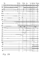
- FIGURE 1 is a block diagram of a memory system which includes an embodiment of the present invention.
- FIGURES 2A and 2B show timing diagrams of several signals that are useful in explaining the operation of the memory system shown in FIGURE 1.
- broad arrows represent busses conveying multiple-bit parallel digital signals and line arrows represent connections conveying single-bit digital signals.
- compensating delays may be required in certain of the signal paths.
- One skilled in the art of digital memory circuit design would know where such delays are needed in a particular system.
- the memory system described below accepts and provides four-bit nibbles at the NTSC sampled data video rate of 14.32 MHz. To simplify the explanation of this memory system, these four-bit nibbles are referred to as pixel values.
- a memory system which operates at 14.32 MHz and uses eight-bit pixel values may be built by configuring two of these memory systems in parallel.
- FIGURE 1 is a block diagram of a video memory system which may be realized as a single 18-pin integrated circuit.
- the pin designations correspond respectively to signal names used in FIGURE 1 as shown in TABLE I.
- the two remaining pins are for coupling the integrated circuit to a source of operating potential and a source of reference potential (e.g. ground).
- the memory system shown in FIGURE 1 may include, for example, a sufficient number of bit storage elements (cells) in the memory cell array 50 to hold 262,144 (2 18 ) four-bit pixel values. This number of cells is sufficient to hold, for example, one field (238,875 four-bit pixel values) of a sampled data NTSC video signal having a sampling frequency of 14.32 MHz (4f c ).
- This memory system is able to accept and supply four-bit pixel values at standard video rates.
- the pixel values applied to the memory system may be written into storage cells addressed by a write address value while other pixel values held in storage cells addressed by an independent read address value are provided by the memory system.
- the write and read address values are incremented as the pixel values are accepted and provided in order to maintain continuous input and output data streams.
- the address values may be changed and read or write operations may be enabled or inhibited by loading address and control values into the memory system via the serial address input terminal SAD. Another function of the control value loaded via the SAD terminal is to allow the memory read and write operations to be synchronized to the signal TAS.
- serial-to-parallel converters 38B through 38E Four-bit pixel values, applied to the data input terminals Dlo through D1 3 , are stored sequentially in respective serial-to-parallel converters 38B through 38E.
- the serial-to-parallel converters 38 collect, for example 32 pixel values during 32 successive periods of a write clock signal, WCK, and then transfer the collected pixel values as a single block of data into buffer latches 40B through 40E respectively. This transfer occurs in a fraction of the next successive clock period.
- the pixel values are transferred from the latches 40 to the memory cell array 50 during several of the ensuing 32 clock periods while new pixel values are loaded into the serial-to-parallel converters 38.
- a block of 32 pixel values is read from the memory cell array 50 over several periods of a read clock signal, RCK, and stored in output buffer latches 52A through 52D. From the latches 52A through 52D, the block of pixel values is transferred to respective parallel-to-serial converters 54A through 54D during a portion of one of the read clock cycles. The parallel-to-serial converters 54 then provide the individual four-bit pixel values, synchronous with the read clock signal, RCK, via the output terminals DOo through D0 3 over the next 32 periods of the signal RCK.
- the addresses applied to the cell array 50 and the control signals which determine when the data are transferred from the serial-to-parallel converters 38 and latches 40 to the memory cell array 50 and from the cell array 50 to the latches 52 and parallel-to-serial converters 54, are generated by circuitry internal to the memory system shown in FIGURE 1.
- This circuitry, the memory sequencing circuitry 22, is controlled by externally provided address and control signal values as outlined below.
- Read and write address values are applied to the SAD input terminal of the memory system as a bit-sequential signal.
- the signal applied to the SAD input terminal is separated into one read address and one write address and stored in the internal read and write address registers 24 and 26 respectively.
- the memory system also includes an automatic refresh function which may, for example, restore all of the data in a predetermined portion of the memory cell array in one operation.
- the refresh address is internally generated and stored in an internal refresh address register 28.
- the memory sequencing circuitry 22 may, for example, sequentially perform a read, a write and a refresh operation on the memory cell array 50 during one 32 clock cycle interval. These operations are timed by the sequencing circuitry 22 to prevent any conflicting access to data in the memory cell array. Generally, during each of the read, write and refresh operations, the address value used to access the memory is incremented by one in address incrementing circuitry 32 and stored into the read, write or refresh address register as appropriate.
- the memory system shown in FIGURE 1 is capable of reading and writing pixel data using the same sequence of successive block address values or using respectively different sequences of successive block address values.
- the memory system may appear to be a one-field-period delay element suitable for use in field or frame based video signal processing circuitry.
- the memory system may appear as a delay element providing a time delay of less than one field period or as a "random access" memory where the pixel data are accessed in blocks of 32 four-bit pixel values.
- the read and write address values and the control value are applied as a bit-serial signal to the serial address input terminal SAD.
- each of the address values is a 13- bit value and the control value is a three-bit value.
- the bit-serial signal is loaded into the address input buffer 10 in synchronism with a serial address clock signal SAS.
- the address input buffer 10 may, for example, be realized as a 29 bit serial input, parallel output shift-register.
- the read and write address values and the control value are applied to the serial input port and provided via parallel output ports of the buffer 10.
- the bits of the read and write address values are interleaved.
- the most significant bits of the two address values are the first two bits of the signal followed by the next most significant bits of the two address values and continuing on to the least significant bits.
- the three-bit control signal is appended to the interleaved addresses following the least significant bits of the two address values.
- the signal TAS is coupled to the read and write address latches 16 and 14 to control the transfer of the read and write address values from the address input buffer 10 to the respective latches 16 and 14.
- Each of the latches 16 and 14 may include, for example, 13 data-type flip-flops arranged as a parallel-in-parallel-out register.
- the address values provided by the buffer 10 are loaded into the latches 16 and 14 on the negative-going edge of the signal TAS.
- FIGURE 2 The timing of an address load and transfer is shown in FIGURE 2.
- the memory system contains pixel data but has no outstanding read, write or refresh operations scheduled.
- the first bit of a new pair of address values ARo and AWo is applied to the address input terminal SAD at time TA o .
- the individual bits of the read address value, AR o , and write address value, AW o , and the three-bit control value are sequentially loaded into the address input buffer 10, one bit per period in the 29 periods of the signal SAS following time TAo.
- the address input buffer 10 contains a 13 bit read address value, a 13 bit write address value and a three-bit control value.
- the read and write address values are transferred to the respective read and write address latches 16 and 14 and the three-bit control value is transferred to the memory sequencing circuitry 22.
- the three control bits, designated RF, WF and MF, from the input buffer 10, and the signal TAS are applied to the memory sequencing circuitry 22 to control the operation of the memory system.
- the bits RF and WF control whether data are read from or written to the pixel storage elements addressed by the respective read and write address values in the respective latches 16 and 14.
- the bit MF determines whether these read and write operations are synchronized by circuitry internal to the memory system or by the externally supplied signal TAS.
- the function of the control signals RF, WF and MF are summarized in Table 2. In the example shown in FIGURE 2A, the three control bits, RF, WF and MF provided at time TA 1 all have values of logic zero.
- data applied to the memory system via the input terminals Dlo through D1 3 after time TA will be written into the pixel storage elements addressed by the newly supplied write address value, AWo; data provided via the output terminal DOo through D0 3 , after a suitable delay (e.g. 32 periods of the signal CLK) will be data from the pixel storage elements addressed by the newly supplied read address value, ARo, and the read and write operations using these address values are initiated by the negative going edge of the signal TAS.
- a suitable delay e.g. 32 periods of the signal CLK
- the read and write address values held by the latches 16 and 14, respectively, are applied to respective first input ports of the multiplexers 20 and 18. Second input ports of the multiplexers 20 and 18 are coupled to the output port of the address incrementing circuitry 32.
- the multiplexers 20 and 18 are controlled by the respective control signals SELR and SELW provided by the memory sequencing circuitry 22.
- the memory sequencing circuitry 22 pulses the signals SELR and SELW, two and one-half master clock pulses after the negative going edge of the signal TAS to condition the respective multiplexers 20 and 18 to apply the address values AR o and AW o held by the respective latches 16 and 14 to the input ports of the read address register 24 and write address register 26, respectively.
- the signals SELR and SELW condition the multiplexers 20 and 18 to apply the address value provided by the address incrementing circuitry 32 to the input port of the respective read and write address registers 24 and 26.
- the read address register 24 and write address register 26 are controlled by respective signals LD1 and LD2 provided by the memory sequencing circuitry 22 to load new read and write address values, respectively, when the signals SELR and SELW are pulsed or when respective incremented read and write address values are available at the output port of the incrementing circuitry 32.
- a 10-bit refresh address value held by a refresh address register 28 is applied to the multiplexer 30.
- the input port of the refresh address register 28 is coupled to the output port of the incrementing circuitry 32.
- the ten least significant bits of the value provided by the incrementing circuit 32 are stored in the refresh address register coincident with a pulse of the signal LD3 provided by the memory sequencing circuitry 22.
- the multiplexer 30 is controlled by a two-bit signal MC provided by the memory sequencing circuitry 22.
- the signal MC conditions the multiplexer to apply either the read address value from register 24, the write address value from register 26 or the refresh address value from register 28 to the memory address register 31.
- the selected address value is loaded into the register 31 coincident with the positive-going edge of signal LD4 provided by the memory sequencing circuitry 22.
- the 13-bit address value held by the memory address register 31 is applied to the address incrementing circuitry 32.
- the circuitry 32 may include, for example, a 13-bit binary adder (not shown) having the value held by the register 31 applied to one input port and a value of one applied to the other input port.
- the address value available at the output port of the incrementing circuitry 32 is applied to the refresh address register 28 and to the second input ports of the multiplexers 18 and 20 as set forth above.
- the memory cell array As a matrix of blocks of pixel cells.
- the matrix has 2 10 (1024) rows and 2 3 (8) columns.
- Each unique combination of a row and column address value corresponds to a respectively different block of 32 four-bit pixel storage cells.
- the ten least significant bits of the address value held by the memory address register 31 are applied to row address decoding circuitry 34 and the three most significant bits are applied to column address decoding circuitry 36.
- the row decoding circuitry 34 which may be of conventional design, decodes the ten least significant bits of the address value to select one of the 1024 rows
- the column decoding circuitry 36 which may be of conventional design, decodes the three most significant bits of the address value to select ore of the eight columns.
- the block of pixel storage cells selected by the row and column decoding circuitry 34 and 36 is gated onto a 32 x 4 (128) bit data bus, I/O, by conventional circuitry.
- the data bus I/O is coupled to the data input gating circuits 42A through 42D and to the data output latches 52A through 52D.
- Data are provided to the memory cell array 50 via the data input terminals Dl o through D1 3 , serial-to-parallel converters 38B through 38E, data input latches 40B through 40E and data input gating circuits 42A through 42D.
- Data applied to the write enable input terminal, WE, and to the four data input terminals Dlo through D1 3 are stored in the respective serial-to-parallel converters 38A through 38E.
- a new bit of data is stored in each of the five serial-to-parallel converters coincident with negative-going edge of each pulse of the clock signal WCK provided by the memory sequencing circuitry 22.
- the signal WCK may be, for example, the logical AND of the system clock signal CLK and an inverted version of the write clock gate signal GW.
- the clock signal WCK is disabled and, so, data values applied to the serial-to-parallel converters 38 are not stored.
- the signal GW is a logic zero, however, the signal WCK is enabled and data are stored in the converters 38 synchronous with the negative-going edges of the clock signal CLK.
- the memory sequencing circuitry 22 counts pulses of the signal WCK, as set forth below, to determine when the data held in the serial-to-parallel converters 38 is to be transferred to the five 32-bit latches 40A through 40E.
- the latches 40A through 40E are controlled by the memory sequencing circuitry 22 to load the 32 four-bit pixel values and the corresponding 32 bits of the signal WE coincident with the positive-going edge of a signal WLD.
- the output values from the 32-bit latches 40B through 40E are applied to respectively different ones of the data input gating circuits 42A through 42D.
- Each of these gating circuits includes, for example, 32 three-state gates (not shown).
- Each of the three-state gates in a gating circuit is connected to a respectively different output terminal of its associated data input latch.
- the output terminals of the three-state gates are coupled to respectively different bit lines of the data bus I/O.
- the 32 three state gates in each of the gating circuits 42 are controlled by the signals generated by respectively different ones of the 32 OR gates 41.
- the OR gates 41 combine a signal ENW and corresponding bit values of the 32-bit signal WE stored in the register 40A in a logical OR function to generate 32 control signals applied to the 32 three-state gates of each of the data input gating circuits 42.
- the memory sequencing circuitry 22 provides a logic zero value for the signal ENW to transfer, to the memory cell array 50, the four-bit pixel values held in the latches 40B through 40E, as masked by the values of the signal WE Held in latch 40A.
- the signal WE masks the pixel values as follows. When a bit of the signal WE is a logic zero, the corresponding three state gates in each of the gating circuits 42A through 42D are enabled to apply the corresponding four-bit pixel value to the data bus I/O of the memory cell array 50. When a bit of the signal WE is a logic one, however, the corresponding three-state gates in each of the input gating circuits 42A through 42D present a high impedance to the data bus I/O.
- a memory read operation proceeds as follows in this embodiment of the invention. Thirty-two four-bit pixel values are transferred from an addressed block of pixel value storage cells in the memory cell array 50 to the data output latches 52A through 52D when the signal ENR, supplied by the memory sequencing circuitry 22, has a value of logic-one.
- Each of the data output latches 52A through 52D may include, for example, 32 data-type flip-flops configured as a parallel-in-parallel-out register.
- the 32 four-bit pixel values held in the latches 52A through 52D are transferred into four 32-bit parallel-to-serial converters 54A through 54D, respectively, coincident with the positive-going edge of a pulse of the signal RLD, supplied by the memory sequencing circuitry 22.
- Each of the parallel-to-serial converters 54A through 54D may include, for example, 32 data type flip-flops configured as a parallel-in-serial-out shift register.
- Each of the parallel-to-serial converters 54 provides one-bit of the 32 four-bit pixel values synchronous with a read clock signal RCK, provided by the memory sequencing circuitry 22.
- the signal RCK may be, for example, the logical AND of the master clock signal CLK and an inverted version of the read clock gate signal GR.
- the memory sequencing circuitry 22 may include, for example, a counter (not shown) which counts the pulses of the signal RCK. This counter is reset when new pixel values are loaded into the parallel-to-serial converters 54.
- the memory sequencing circuitry 22 pulses the signal RLD to load 32 new pixel values into the converters 54 and resets the RCK counter (not shown).
- the output terminals of the four parallel-to-serial converters 54A through 54D are coupled to respective three-state gate circuits 56A through 56D.
- the three-state gate circuits 56 are controlled by an externally supplied output enable signal OE.
- the signal OE has a value of logic one
- the three state gate circuits 56 present a high impedance at the output terminals DOo through D0 3 .
- the circuits 56 present the logic values, applied to their input terminals, at the output terminals DOo through D0 3 .
- the memory sequencing circuitry 22 In addition to controlling the reading of data from, and writing of data into the memory cell array 50, the memory sequencing circuitry 22 also controls the periodic refreshing of data values stored in the memory cell array 50. To understand how the refresh operation occurs, it is helpful to first understand why the data values are refreshed.
- the memory cell array 50 is composed of 2 2 ° (1,048,576) dynamic bit-storage cells arranged as 2 13 (8,192) blocks of 32 four-bit pixel storage cells. A datum is stored in one of these dynamic bit-storage cells as a charge or absence of a charge on a capacitor (not shown). This charge is not stable and tends to dissipate over time.
- the memory cell array 50 used in the present embodiment of the invention may be considered to be organized as a matrix having 1024 rows, 256 columns and four bit planes.
- the four bit planes correspond, respectively, to the four bits of pixel values.
- the 256 columns on each bit plane are organized in eight groups where each group includes 32 columns, all 32 columns in a given group have the same column address. In this memory organization, each of the 256 columns in each of the four bit planes has a separate sense amplifier (not shown).
- each refresh operation restores 256 pixel values (1024 bits of data). All of the data in the memory cell array 50 may be refreshed in 1024 refresh operations (i.e. a refresh operation for each row in the matrix).
- the automatic refresh system used in the memory system shown in FIGURE 1 refreshes all of the bit-storage cells in the memory cell array in less than 5 milliseconds. To do this, one row of the memory cell array is refreshed every 64 cycles of the clock signal CLK.
- a typical refresh operation proceeds as follows. Once a refresh address has been established, the memory sequencing circuitry 22 pulses a signal REF applied to the column decoding circuitry 36 and to the memory cell array 50 to activate the sense amplifiers in all 256 columns on all four-bit planes of the memory cell array 50 and to inhibit the gating of the sense amplifiers to the data bus.
- the sense-amplifiers read and restore the data held in each of the dynamic bit storage cells in the addressed row.
- the structure of the individual memory bit storage cells and of the sense amplifiers depends on the technology (e.g. NMOS or CMOS) used to implement the memory system and may also depend on factors such as the desired data access time and the power dissipation for the memory system.
- Exemplary circuitry for implementing the memory storage cells, sense amplifiers and address decoders is shown in an article by K. Kimura et al. entitled “Power Reduction Techniques in Megabit DRAM's", IEEE Journal of Solid-State Circuits, Vol. SC-21, No. 3, June 1986, pp. 381-389.
- FIGURES 2A and 2B are signal timing diagrams which are useful for illustrating the operation of the memory system under the control of the memory sequencing circuitry 22.
- the timing values shown in these figures are specific to this embodiment of the invention. They are provided to illustrate one possible implementation of the invention.
- the master clock signal CLK used in this embodiment of the invention has a frequency of 14.32 MHz, 4f c in the NTSC system.
- the other clock signals, SAS, WCK and RCK are all derived from this master clock signal.
- the timing diagrams in FIGURES 2A and 2B show a series of memory functions which illustrate the operation of the memory sequencing circuitry 22.
- time values are marked across the top of the FIGURES 2A and 2B.
- the time values TAo, TA 1 , TA 2 and TA 3 designate times at which memory address events occur, either the start or finish of an address load operation.
- the time values TC o through TC 1 3 mark the boundaries of internal memory cycles, each memory cycle spans eight periods of the master clock signal CLK. Memory operations which affect the memory cell array 50 (i.e. memory read, write and refresh) occur during respectively different memory cycles and are initiated on the memory cycle boundaries.
- the time values TB o , TB 1 and TB 2 mark times at which data are transferred from the serial-to-parallel converters 38 to the data input latches 40 and/or times at which data are transferred from the data output latches 52 to the parallel-to-serial converter 54.
- a read address value AR o and a write address AW o are loaded into the memory system.
- Read operations using AR o and AR 0+1 are initiated at times TC o and TC s , respectively.
- a write operation using memory address AW o is initiated at time TC 4 .
- a read address value AR 1 and write address value AW 1 are loaded into the memory system.
- a memory write operation using address AW 1 is initiated at time TC 8 and a read operation using address AR 1 is initiated at time TC 9 .
- Memory refresh operations are initiated at times TC 1 and TC 10 .
- the memory sequencing circuitry 22 pulses the signals SELR and SELW to condition the respective multiplexers 20 and 18 to apply these address values to the read and write address registers 24 and 26, respectively. Shortly after the positive going edges of the signals SELR and SELW, the circuitry 22 pulses the signals LD1 and LD2 to load the respective address values ARo and AWo into the respective read and write address registers 24 and 26.
- the MF bit of the control value applied to the memory sequencing circuitry 22 at time TA 1 is a logic zero. Consequently, the read and write operations which uses the address values supplied at TA 1 are synchronized to the signal TAS. In the present embodiment of the invention this is accomplished by resetting the counters (not shown) in the memory sequencing circuitry 22 which count pulses of the respective signals WCK and RCK, and by scheduling a memory read operation. To indicate that a read write or refresh operation is scheduled, the memory sequencing circuitry 22 may include, for example, three set-reset latches (not shown).
- the first, second and third latches are set by the circuitry 22 to schedule a read, a write and a refresh operation, respectively and are reset by the circuitry 22 when the corresponding operation is initiated.
- a priority is established such that a write operation has the highest priority followed by a read operation and then a refresh operation. This priority assignment is somewhat arbitrary although it is generally desirable for refresh operations to have the lowest priority.
- the 32 four-bit pixel values, applied to the data input terminals Dlo through D1 3 over the 32 periods of the signal WCK following the negative going edge of the signal TAS are sequentially stored in the serial-to-parallel converters 38B through 38E.
- the input terminal WE is held at a logic zero value so that none of the four-bit pixel values are masked from being written into the memory cell array 50 as set forth above.
- the entry of pixel data into the serial-to-parallel converters 38 is started at time TA, when the value of the externally supplied write clock gate signal GW is changed to a logic zero.
- the time TC o is at the start of the first memory cycle shown in FIGURE 2A.
- a read operation and a refresh operation are scheduled. According to the priority scheme set forth above, the read operation is initiated first.
- the first step in the read operation is to change the signal MC to condition the multiplexer 30 to apply the read address value ARo from the read address register 24 to the memory address register 31.
- the signal LD4 is pulsed to load the read address value into the memory address register 31.
- the address value held by the register 31 is applied to the row decoding circuitry 34 and column decoding circuitry 36 to select a block of pixel storage cells from the memory cell array 50.
- the signal ENR is pulsed for five periods of the master clock signal CLK. While the signal ENR has a logic one value, the data output latches 52 are gated onto the bus I/O.
- the 32 four-bit pixel values held in the addressed block of pixel storage cells are transferred to the output latches 52.
- the signal LD1 is pulsed to load the incremented read address value from the incrementing circuitry 32 into the read address register 24.
- the data held in the latches 52 at time TC 1 is not transferred to the parallel-to-serial converters until a time 32 periods of the signal CLK after time TA 1 . This time is shortly after time TBo in FIGURE 2A.
- the delay of 32 master clock periods between the completion of the read operation and the availability of the pixel data at the output terminals DOo through D0 3 allows the memory sequencing circuitry 22 to initiate the read operation, which was initiated in the present example at time TCo, either at time TCo, time TC 1 or time TC 2 . This flexibility ensures that any potential conflict between read, write and refresh operations can be resolved before the data read from the memory cell array 50 is expected at the output port.
- the portion of the read operation which accesses the memory cell array 50 is complete.
- the refresh operation which has been scheduled since time TC o , is initiated by the memory sequencing circuitry 22.
- the circuitry 22 first changes the state of the signal MC to condition the multiplexer 30 to apply the refresh address value from the refresh address register 28 to the memory address register 31.
- the circuitry 22 then pulses the signal LD4, one master clock period after time TC,, to load, the refresh address value into the register 31.
- a pulse having a width of three clock periods is applied, as the signal REF, to the column decoding circuitry 36 and to the memory cell array 50, to refresh the addressed row of bit-storage cells in each of the four bit planes of the memory cell array 50.
- the signal LD3 is pulsed to load the ten least significant bits of the incremented refresh address value, as provided by the incrementing circuitry 32, into the refresh address register 28.
- the refresh operation is complete.
- a new address and control value is applied to the serial address input terminal SAD and loaded into the input buffer 10 synchronous with the clock signal SAS.
- This address load operation occurs in the same sequence of steps as the one set forth above and is not described in detail.
- a new read address value, AR1, and a new write address value, AW are loaded into the read address latch 16 and write address latch 14, respectively, and new control values RF, WF and MF, having respective values of zero, zero and one, are loaded into the memory sequencing circuitry 22.
- new control values RF, WF and MF having respective values of zero, zero and one
- a read operation and a refresh operation have been performed on the memory cell array 50 and no write operation is scheduled, since only 19 four-bit pixel values have been loaded into the serial-to-parallel converters 38. Since no memory operations are scheduled at time TC 2 or at time TC 3 , none are performed.
- the 32nd pixel value is loaded into the serial-to-parallel converters 38.
- the memory sequencing circuitry 22 pulses the signal WLD to transfer the 32 four-bit pixel values from the converters 38 to the input latches 40.
- the circuitry 22 resets its internal counter (not shown) which tallies the pixels applied to the serial-to-parallel converters 38 and schedules a memory write operation.
- the time at which the contents of the serial-to-parallel converters 38 are to be transferred to the latches 40 is 32 periods of the master clock signal CLK after time TA 1 . This is also the time at which the pixel data values read from the memory cell array 50 having the address AR o are to be supplied via the output terminals DOo through D0 3 . Accordingly, at the same time that the circuitry 22 pulses the signal WLD, it also pulses the signal RLD to transfer the contents of the output buffer latches 52 to the parallel-to-serial converters 54. At this time, the circuitry 22 also schedules the next read operation.
- the externally supplied read clock gate signal GR and output enable signal OE are changed to have logic zero values, enabling the signal RCK and the three-state gates 56.
- the 32 four-bit pixel values held in the parallel to serial converters 54 are provided via the output terminals DOo through D0 3 .
- a read operation and a write operation are scheduled. Since the write operation has a higher priority it is initiated by the memory sequencing circuitry 22.
- the signal MC is changed by the circuitry 22 to condition the multiplexer 30 to apply the write address value AW o , held in the write address register 26, to the memory address register 31.
- the circuitry 22 pulses the signal LD4 to load the address value AWo into the register 31.
- the memory sequencing circuitry 22 changes the signal ENW to a logic zero value, for five periods of the master clock signal, to gate the 32 four-bit pixel values held by the latches 40 onto the data bus I/O.
- the memory write operation is complete and a memory read operation is scheduled.
- the read and write address values, AR 1 and AW1 supplied at time TA 3 , one-half of one master clock cycle before time TC s , have not yet been propagated to the read and write address registers 24 and 26, respectively. Consequently, the read operation initiated at time TC 5 uses the incremented read address value (i.e. ARo + 1) from the read address register 24 rather than the newly provided read address value AR 1 .
- the address value ARo + 1 is transferred from the read address register 24 to the memory address register 31 by the signal LD4 emitted by the memory sequencing circuitry 22 one master clock period after time TCs. Two and one-half master clock periods after time TC 5 (or three clock periods after time TA 3 ) the newly provided read and write address values are loaded into the respective read and write address registers 24 and 26 by the memory sequencing circuitry 22 by pulsing the signals SELR, SELW, LD1 and LD2 as set forth above.
- the read operation initiated at time TC 5 proceeds in the same manner as the read operation which was initiated at time TCo except that the memory sequencing circuitry 22 does not pulse the signal LD1 seven master clock cycles after TC 5 to load the incremented address value into the register 24.
- the memory sequencing circuitry disables the signals LD1 and LD2 to prevent the newly loaded address values AR 1 and AW 1 from being overwritten by the incremented address value from a read or write operation which may be in progress as the new address values are supplied.
- the signals LD1 and LD2 are only disabled when the control value MF of the newly loaded address and control signal is a logic one. In this instance, the read and write operations using the newly supplied address values occur only after any currently scheduled read and write operations.
- the sequencing circuitry 22 schedules a new read operation which overrides any currently scheduled read operation. In addition, it resets the internal counter which tallies the pulses of the signal WCK, postponing the next memory write operation.
- Time TB 1 is 32 master clock periods after time TBo.
- 32 four-bit pixel values have been stored in the serial-to-parallel converters 38 and 32 four-bit pixel values have been provided by the parallel-to-serial converters 54. Consequently, coincident with the positive going edge of the first pulse of the signal CLK following time TB1, the memory sequencing circuitry 22 pulses the signals RLD and WLD to transfer, respectively, the 32 four-bit pixel values stored in the output latches 52 into the parallel-to-serial converters 54 and the 32 four-bit pixel values held in the serial-to-parallel converters 38 into the input latches 40.
- the memory sequencing circuitry 22 also schedules a read operation and a write operation, one master clock period after time TB 1 .
- the four-bit pixel values applied to the data input terminals Dlo through D1 3 between time TB 1 and TB 2 are written into the block of pixel value storage cells which is addressed by the write address value AW 1 .
- these pixels are to be subsampled in a one-to-two ratio. This subsampling may be performed, for example, to compress the lines of pixel data stored in the memory cell array 50 by one-half to produce a compressed image for a pix-in-pix feature.
- the subsampling is achieved by applying a bilevel signal, having a frequency that is half the frequency of the master clock signal, as the write clock gate signal GW.
- the signal WCK is the logical AND of the master clock signal CLK and an inverted version of the signal GW.
- the signal WCK determines which pixel values are loaded into the serial-to-parallel converters 38. It is also used by the memory sequencing circuitry 22 to determine when to transfer the collected pixel values to the input latches 40.
- the signal WCK after time TB 1 is a clock signal having a 25% duty cycle and a frequency that is one-half of the frequency of the signal CLK. Responsive to this signal, the serial-to-parallel converters store only every other one of the four-bit pixel values applied to the input terminals Dlo through D1 3 . The pixel values that are stored are those occurring coincident with the negative-going edges of the clock signal WCK.
- a write request and a read request are pending.
- the write request is initiated at time TC 8 .
- the 32 four-bit pixel values applied to the memory system in the interval between TBo and TB 1 are written into the block of pixel storage cells that is addressed by the write address value AW 1 loaded at time TA 3 .
- This write operation is performed in the same manner as the one that was initiated at time TC 4 . Accordingly, it is not described in detail.
- Time TC 8 is 64 master clock-cycles after time TC o , the time that the previous refresh operation was scheduled. Since the memory system is designed to refresh one row of bit storage cells every 64 master clock cycles, a refresh operation is scheduled at time TC 8 .
- the memory sequencing circuitry 22 initiates a read operation to transfer the 32 four-bit pixel values, addressed by the read address value, AR1, from the memory cell array 50 into the output latches 52.
- This read operation is performed in the same manner as the one that was initiated at time TCo and, so, is not described in detail.
- the refresh operation which was scheduled at time TC 8 , is performed at time TC 10 .
- This refresh operation proceeds in the same manner as the one initiated at time TC,, consequently, it is not described in detailed.
- the time TB 2 is 32 periods of the clock signal RCK after time TBi.
- all the 32 four-bit pixel values which had been transferred to the parallel-to-serial converters 54 shortly after time TB 1 have been provided by the converters 54 via the output terminals DOo through D0 3 .
- the memory sequencing circuitry 22 pulses the signal RLD to transfer the 32 four-bit pixel values held in the latches 52 into the parallel-to-serial converters 54. In this example, these values are to be provided at the output terminals DOo through D0 3 at one-half the rate at which the prior pixel values were supplied.
- the expansion of the lines of samples is accomplished by changing the read clock gate signal, GR, to be a bilevel signal having a frequency that is one-half the frequency of the signal CLK.
- This signal, GR changes the signal RCK to have a 25% duty cycle and a frequency one-half of the frequency of the signal CLK.
- the parallel-to-serial converters 54 provide the 32 four-bit pixel values at the desired rate.
- the memory sequencing circuitry 22 schedules read and write operations after counting 32 pulses of the respective signals RCK and WCK, no new write operation will be scheduled until a time (not shown) 64 master clock cycles after TB 1 and no new read operation will be scheduled until a time (not shown) 64 master clock cycles after TB 2 .
- the read clock gate signal GR and write clock gate signal GW can be used to control when, and at what rate, data are respectively read from and written into the memory system shown in FIGURE 1.
- the clock signals which load the values into the serial-to-parallel converters 38 and provide values from the parallel-to-serial converters 54 are synchronized to the master clock signal because transfers occur only on the edges of master clock pulses.
- the actual data input and output may be otherwise asynchronous. Data may be applied to or provided by the memory system at any frequency that is a rational fraction of the master clock frequency.
- this memory system is described in the context of video signal processing, it is contemplated that it may also be used in computer data processing applications. For example, the ability to simultaneously and semi-synchronously write and read continuous data streams at respectively different data rates may make this memory system desirable as a data buffer between a microprocessor and a peripheral device, such as a printer, or as an emulator for a mechanical mass storage device, e.g. as a "RAM DISK" device.
Landscapes
- Engineering & Computer Science (AREA)
- Microelectronics & Electronic Packaging (AREA)
- Computer Hardware Design (AREA)
- Multimedia (AREA)
- Signal Processing (AREA)
- Dram (AREA)
Claims (5)
Applications Claiming Priority (2)
| Application Number | Priority Date | Filing Date | Title |
|---|---|---|---|
| US07/008,695 US4823302A (en) | 1987-01-30 | 1987-01-30 | Block oriented random access memory able to perform a data read, a data write and a data refresh operation in one block-access time |
| US8695 | 1987-01-30 |
Publications (3)
| Publication Number | Publication Date |
|---|---|
| EP0280882A2 EP0280882A2 (de) | 1988-09-07 |
| EP0280882A3 EP0280882A3 (en) | 1990-01-17 |
| EP0280882B1 true EP0280882B1 (de) | 1994-05-11 |
Family
ID=21733144
Family Applications (1)
| Application Number | Title | Priority Date | Filing Date |
|---|---|---|---|
| EP88101323A Expired - Lifetime EP0280882B1 (de) | 1987-01-30 | 1988-01-29 | Blockorganisierter RAM-Speicher, fähig, um in einer Blockzugriffszeit Daten zu Lesen, zu Schreiben und Aufzufrischen |
Country Status (5)
| Country | Link |
|---|---|
| US (1) | US4823302A (de) |
| EP (1) | EP0280882B1 (de) |
| KR (1) | KR950010458B1 (de) |
| CA (1) | CA1299738C (de) |
| DE (1) | DE3889480T2 (de) |
Cited By (1)
| Publication number | Priority date | Publication date | Assignee | Title |
|---|---|---|---|---|
| CN1307647C (zh) * | 2000-07-07 | 2007-03-28 | 睦塞德技术公司 | 动态随机存取存储器、存储器器件及其执行读命令的方法 |
Families Citing this family (24)
| Publication number | Priority date | Publication date | Assignee | Title |
|---|---|---|---|---|
| US5283885A (en) * | 1988-09-09 | 1994-02-01 | Werner Hollerbauer | Storage module including a refresh device for storing start and stop refresh addresses |
| JPH0283899A (ja) * | 1988-09-20 | 1990-03-23 | Fujitsu Ltd | 半導体記憶装置 |
| US4920407A (en) * | 1989-01-03 | 1990-04-24 | Gte Laboratories Incorporated | Composite video frame store |
| US5167020A (en) * | 1989-05-25 | 1992-11-24 | The Boeing Company | Serial data transmitter with dual buffers operating separately and having scan and self test modes |
| US5206834A (en) * | 1989-10-14 | 1993-04-27 | Mitsubishi Denki Kabushiki Kaisha | Semiconductor memory device performing last in-first out operation and the method for controlling the same |
| US5633829A (en) * | 1990-03-09 | 1997-05-27 | Mitsubishi Denki Kabushiki Kaisha | Serial access memory device capable of controlling order of access to memory cell areas |
| TW198135B (de) * | 1990-11-20 | 1993-01-11 | Oki Electric Ind Co Ltd | |
| JP3100622B2 (ja) * | 1990-11-20 | 2000-10-16 | 沖電気工業株式会社 | 同期型ダイナミックram |
| US5386531A (en) * | 1991-05-15 | 1995-01-31 | International Business Machines Corporation | Computer system accelerator for multi-word cross-boundary storage access |
| US5319606A (en) * | 1992-12-14 | 1994-06-07 | International Business Machines Corporation | Blocked flash write in dynamic RAM devices |
| US5493530A (en) * | 1993-08-26 | 1996-02-20 | Paradigm Technology, Inc. | Ram with pre-input register logic |
| US5533187A (en) * | 1993-10-29 | 1996-07-02 | Sun Microsystems, Inc | Multiple block mode operations in a frame buffer system designed for windowing operations |
| US5504855A (en) * | 1993-10-29 | 1996-04-02 | Sun Microsystems, Inc. | Method and apparatus for providing fast multi-color storage in a frame buffer |
| WO1995012164A2 (en) * | 1993-10-29 | 1995-05-04 | Sun Microsystems, Inc. | Frame buffer system designed for windowing operations |
| EP0677200B1 (de) * | 1993-10-29 | 2002-04-03 | Sun Microsystems, Inc. | Verschiebungsgeschwindigkeitserhöhung in einem rasterpuffer |
| US5946469A (en) * | 1995-11-15 | 1999-08-31 | Dell Computer Corporation | Computer system having a controller which emulates a peripheral device during initialization |
| JPH09161478A (ja) * | 1995-12-12 | 1997-06-20 | Mitsubishi Electric Corp | 半導体記憶装置 |
| US5740116A (en) * | 1995-12-22 | 1998-04-14 | Townsend And Townsend And Crew, Llp | Current limiting during block writes of memory circuits |
| KR100198541B1 (ko) | 1996-08-26 | 1999-06-15 | 구자홍 | 영상 프레임 데이터를 일 메모리에 저장하는 방법 |
| US5982453A (en) * | 1996-09-25 | 1999-11-09 | Thomson Consumer Electronics, Inc. | Reduction of visibility of spurious signals in video |
| US5903916A (en) * | 1996-12-16 | 1999-05-11 | Intel Corporation | Computer memory subsystem and method for performing opportunistic write data transfers during an access latency period within a read or refresh operation |
| TW430815B (en) * | 1998-06-03 | 2001-04-21 | Fujitsu Ltd | Semiconductor integrated circuit memory and, bus control method |
| US6938142B2 (en) | 2002-08-28 | 2005-08-30 | Micron Technology, Inc. | Multi-bank memory accesses using posted writes |
| CN111128281B (zh) * | 2018-10-31 | 2024-06-21 | 长鑫存储技术有限公司 | 集成电路结构和存储器 |
Family Cites Families (8)
| Publication number | Priority date | Publication date | Assignee | Title |
|---|---|---|---|---|
| FR121860A (de) * | 1973-07-19 | |||
| US4321695A (en) * | 1979-11-23 | 1982-03-23 | Texas Instruments Incorporated | High speed serial access semiconductor memory with fault tolerant feature |
| GB2084361B (en) * | 1980-09-19 | 1984-11-21 | Sony Corp | Random access memory arrangements |
| GB2098021B (en) * | 1981-05-06 | 1985-06-19 | Sony Corp | Digital television apparatuses |
| US4435792A (en) * | 1982-06-30 | 1984-03-06 | Sun Microsystems, Inc. | Raster memory manipulation apparatus |
| JPS6072020A (ja) * | 1983-09-29 | 1985-04-24 | Nec Corp | デュアルポ−トメモリ回路 |
| EP0179605B1 (de) * | 1984-10-17 | 1992-08-19 | Fujitsu Limited | Halbleiterspeicheranordnung mit einer seriellen Dateneingangs- und Ausgangsschaltung |
| JPS61239491A (ja) * | 1985-04-13 | 1986-10-24 | Fujitsu Ltd | 電子装置 |
-
1987
- 1987-01-30 US US07/008,695 patent/US4823302A/en not_active Expired - Lifetime
-
1988
- 1988-01-28 CA CA000557613A patent/CA1299738C/en not_active Expired - Lifetime
- 1988-01-29 EP EP88101323A patent/EP0280882B1/de not_active Expired - Lifetime
- 1988-01-29 DE DE3889480T patent/DE3889480T2/de not_active Expired - Fee Related
- 1988-01-29 KR KR1019880000734A patent/KR950010458B1/ko not_active Expired - Fee Related
Cited By (1)
| Publication number | Priority date | Publication date | Assignee | Title |
|---|---|---|---|---|
| CN1307647C (zh) * | 2000-07-07 | 2007-03-28 | 睦塞德技术公司 | 动态随机存取存储器、存储器器件及其执行读命令的方法 |
Also Published As
| Publication number | Publication date |
|---|---|
| KR880009519A (ko) | 1988-09-15 |
| EP0280882A2 (de) | 1988-09-07 |
| DE3889480T2 (de) | 1994-12-01 |
| KR950010458B1 (ko) | 1995-09-18 |
| DE3889480D1 (de) | 1994-06-16 |
| EP0280882A3 (en) | 1990-01-17 |
| US4823302A (en) | 1989-04-18 |
| CA1299738C (en) | 1992-04-28 |
Similar Documents
| Publication | Publication Date | Title |
|---|---|---|
| EP0276871B1 (de) | Video-Doppelzugriffsspeichersystem mit bitseriellem Adresseneingangstor | |
| EP0280882B1 (de) | Blockorganisierter RAM-Speicher, fähig, um in einer Blockzugriffszeit Daten zu Lesen, zu Schreiben und Aufzufrischen | |
| EP0276870B1 (de) | Video-Doppelzugriffsspeichersystem mit einem halbsynchronen Dateneingang und Datenausgang | |
| US5093807A (en) | Video frame storage system | |
| EP0208325B1 (de) | Bildspeicher | |
| US4646270A (en) | Video graphic dynamic RAM | |
| JP2740097B2 (ja) | クロック同期型半導体記憶装置およびそのアクセス方法 | |
| JPS62152050A (ja) | 半導体メモリ | |
| US4961169A (en) | Method of and apparatus for generating variable time delay | |
| US4972376A (en) | Self-refresh system for use in a field memory device operating without reliance upon external control | |
| US5587962A (en) | Memory circuit accommodating both serial and random access including an alternate address buffer register | |
| KR0133078B1 (ko) | 동기식 다이나믹 랜덤 억세스 메모리 장치 및 이를 사용하여 기록을 행하는 방법 | |
| US5835418A (en) | Input/output buffer memory circuit capable of minimizing data transfer required in input and output buffering operations | |
| JPH07101551B2 (ja) | 映像記憶装置 | |
| JPH036595B2 (de) | ||
| JPH01263777A (ja) | 画像メモリのシリアルバッファ装置 | |
| JPH0236483A (ja) | 画像用メモリ装置 | |
| JPH0489688A (ja) | デュアルポート・グラフィック・バッファ |
Legal Events
| Date | Code | Title | Description |
|---|---|---|---|
| PUAI | Public reference made under article 153(3) epc to a published international application that has entered the european phase |
Free format text: ORIGINAL CODE: 0009012 |
|
| AK | Designated contracting states |
Kind code of ref document: A2 Designated state(s): DE FR GB IT |
|
| RAP1 | Party data changed (applicant data changed or rights of an application transferred) |
Owner name: RCA LICENSING CORPORATION |
|
| PUAL | Search report despatched |
Free format text: ORIGINAL CODE: 0009013 |
|
| AK | Designated contracting states |
Kind code of ref document: A3 Designated state(s): DE FR GB IT |
|
| 17P | Request for examination filed |
Effective date: 19900712 |
|
| 17Q | First examination report despatched |
Effective date: 19920116 |
|
| RAP1 | Party data changed (applicant data changed or rights of an application transferred) |
Owner name: RCA THOMSON LICENSING CORPORATION |
|
| GRAA | (expected) grant |
Free format text: ORIGINAL CODE: 0009210 |
|
| AK | Designated contracting states |
Kind code of ref document: B1 Designated state(s): DE FR GB IT |
|
| REF | Corresponds to: |
Ref document number: 3889480 Country of ref document: DE Date of ref document: 19940616 |
|
| ITF | It: translation for a ep patent filed | ||
| ET | Fr: translation filed | ||
| PLBE | No opposition filed within time limit |
Free format text: ORIGINAL CODE: 0009261 |
|
| STAA | Information on the status of an ep patent application or granted ep patent |
Free format text: STATUS: NO OPPOSITION FILED WITHIN TIME LIMIT |
|
| 26N | No opposition filed | ||
| REG | Reference to a national code |
Ref country code: GB Ref legal event code: 732E |
|
| REG | Reference to a national code |
Ref country code: GB Ref legal event code: IF02 |
|
| REG | Reference to a national code |
Ref country code: FR Ref legal event code: D6 |
|
| REG | Reference to a national code |
Ref country code: GB Ref legal event code: 746 Effective date: 20030228 |
|
| PGFP | Annual fee paid to national office [announced via postgrant information from national office to epo] |
Ref country code: GB Payment date: 20051123 Year of fee payment: 19 |
|
| PGFP | Annual fee paid to national office [announced via postgrant information from national office to epo] |
Ref country code: DE Payment date: 20051125 Year of fee payment: 19 |
|
| PGFP | Annual fee paid to national office [announced via postgrant information from national office to epo] |
Ref country code: FR Payment date: 20060130 Year of fee payment: 19 |
|
| PGFP | Annual fee paid to national office [announced via postgrant information from national office to epo] |
Ref country code: IT Payment date: 20060131 Year of fee payment: 19 |
|
| PG25 | Lapsed in a contracting state [announced via postgrant information from national office to epo] |
Ref country code: DE Free format text: LAPSE BECAUSE OF NON-PAYMENT OF DUE FEES Effective date: 20070801 |
|
| GBPC | Gb: european patent ceased through non-payment of renewal fee |
Effective date: 20070129 |
|
| REG | Reference to a national code |
Ref country code: FR Ref legal event code: ST Effective date: 20070930 |
|
| PG25 | Lapsed in a contracting state [announced via postgrant information from national office to epo] |
Ref country code: GB Free format text: LAPSE BECAUSE OF NON-PAYMENT OF DUE FEES Effective date: 20070129 |
|
| PG25 | Lapsed in a contracting state [announced via postgrant information from national office to epo] |
Ref country code: FR Free format text: LAPSE BECAUSE OF NON-PAYMENT OF DUE FEES Effective date: 20070131 |
|
| PG25 | Lapsed in a contracting state [announced via postgrant information from national office to epo] |
Ref country code: IT Free format text: LAPSE BECAUSE OF NON-PAYMENT OF DUE FEES Effective date: 20070129 |