EP0280381B1 - Anti-Larsen-Pegelregelungsanordnung in einem Verstärker eines Fernsprechapparats - Google Patents
Anti-Larsen-Pegelregelungsanordnung in einem Verstärker eines Fernsprechapparats Download PDFInfo
- Publication number
- EP0280381B1 EP0280381B1 EP88200355A EP88200355A EP0280381B1 EP 0280381 B1 EP0280381 B1 EP 0280381B1 EP 88200355 A EP88200355 A EP 88200355A EP 88200355 A EP88200355 A EP 88200355A EP 0280381 B1 EP0280381 B1 EP 0280381B1
- Authority
- EP
- European Patent Office
- Prior art keywords
- gain
- control means
- output
- comparator
- capacitor
- Prior art date
- Legal status (The legal status is an assumption and is not a legal conclusion. Google has not performed a legal analysis and makes no representation as to the accuracy of the status listed.)
- Expired - Lifetime
Links
Images

Classifications
-
- H—ELECTRICITY
- H03—ELECTRONIC CIRCUITRY
- H03G—CONTROL OF AMPLIFICATION
- H03G3/00—Gain control in amplifiers or frequency changers without distortion of the input signal
- H03G3/20—Automatic control
- H03G3/30—Automatic control in amplifiers having semiconductor devices
-
- H—ELECTRICITY
- H03—ELECTRONIC CIRCUITRY
- H03G—CONTROL OF AMPLIFICATION
- H03G1/00—Details of arrangements for controlling amplification
- H03G1/0005—Circuits characterised by the type of controlling devices operated by a controlling current or voltage signal
- H03G1/0088—Circuits characterised by the type of controlling devices operated by a controlling current or voltage signal using discontinuously variable devices, e.g. switch-operated
-
- H—ELECTRICITY
- H04—ELECTRIC COMMUNICATION TECHNIQUE
- H04M—TELEPHONIC COMMUNICATION
- H04M9/00—Arrangements for interconnection not involving centralised switching
- H04M9/08—Two-way loud-speaking telephone systems with means for conditioning the signal, e.g. for suppressing echoes for one or both directions of traffic
Definitions
- the present invention relates to a gain control circuit of an amplifier for listening by loudspeaker in a device also comprising a microphone and its associated amplifier, in particular for the purpose of eliminating the Larsen effect, a circuit consisting essentially of a feedback loop reducing the gain of the loudspeaker amplifier when the signal from the microphone exceeds a determined threshold.
- the invention also relates to the application of this gain control circuit to a telephone set with amplified listening by loudspeaker. It is well known that in all systems comprising both a speaker powered by its amplifier and a microphone whose signal is applied more or less directly to the amplifier, there is a risk of oscillation by Larsen effect. due to the acoustic coupling between the speaker and the microphone. This is the case for example of a telephone set provided with an amplified listening, case to which the invention is addressed more particularly but not exclusively.
- the Larsen effect detection circuit must be very selective to distinguish an oscillation signal from an audio signal. high amplitude but momentary like an ambient noise or a shock on the microphone.
- the invention aims to provide a suitable control circuit for the gain of the loudspeaker amplifier, avoiding relaxation and which would use essentially integrable circuits.
- control circuit in accordance with the preliminary paragraph, characterized in that the feedback loop comprising first control means, controlling a gain reduction of the listening amplifier by loudspeaker with a first time constant, and said predetermined threshold being a first threshold, it also comprises second control means comparing the signal coming from the microphone with a second threshold, lower than said first threshold, which control a reduction in gain with a second time constant lower than the first, from the moment when the gain has been reduced below a reference gain value by said first means, while they remain inactive when the gain remains greater than said reference value.
- said first control means are normally sufficient to properly attenuate the amplification of the listening signal by loudspeaker, if necessary, and to regulate the amplification of the usual way.
- any acoustic signal which arrives at the microphone with a high level but for a short duration, that is to say a duration less than the first time constant, does not trigger the second means, in contrast to the instability caused by the 'Larsen effect which generates, by acoustic coupling, a strong microphone signal and for a generally long duration depending on the acoustic coupling conditions between the loudspeaker and the microphone.
- the first control means have led to lowering the gain below the determined value taken as a reference, which occurs after the first time constant
- the second control means come into action with a time constant set significantly more lower than the time constant of the first means, and the gain is quickly reduced to the value necessary for the regulation to operate by comparison with the second threshold.
- the second threshold is chosen to be lower than the first threshold, relaxation does not occur and the circuit returns to normal gain conditions only when the microphone signal drops below the second threshold, i.e. in practice when the cause of the oscillation has disappeared.
- the gain control circuit is characterized in that the gain of the loudspeaker amplifier is controlled by the charging voltage of a capacitor, permanently charged through a current source and in that the first and second control means have their outputs which cause the discharge of this capacitor via respectively a first and a second discharge resistance, the first discharge resistance having a higher value than that of the second discharge resistor.
- control circuit is further characterized in that the capacitor is charged from the most positive potential of the circuit, in that said first and second control means discharge the capacitor by their terminal.
- output which is of the NPN transistor type (or N channel MOS), with open collector (or open drain), and in that the first discharge resistance of the capacitor is arranged in series with the second discharge resistance.
- Transistors of this type have the advantage of being easily integrated.
- open collector type outputs makes it possible to couple the outputs of the first and second control means through their respective discharge resistance since the high impedance state of the output of one of the control means remains without effect on the output of the other.
- a variant of this embodiment dispenses with the use of discharge resistors when the first and second control means have their output which operates at a discharge current limited to a fixed value; the output current of the first means is then fixed at a lower value than the value of the output current of the second means, and the outputs in question are connected in parallel on the capacitor.
- a particular embodiment of the invention is characterized in that the first control means comprise a first comparator whose positive input receives the signal from the microphone after amplification, whose negative input is brought to a first voltage reference which being lower than the continuous level of the signal from the microphone, defines with respect to this level said first threshold, and the output of which constitutes the output of said first control means, in that the second control means comprise a second, a third and fourth comparator, all with open collector type output of an NPN transistor, in that the second comparator has its negative input which receives the signal from the microphone after amplification, and its positive input which is brought to a second reference voltage slightly higher than the first reference voltage but nevertheless lower than the continuous level of the signal coming from the microphone and which defines with respect to this level said second threshold, in that the output of the second comparator is on the one hand connected to the intermediate point of a first impedance bridge which is also connected between the extreme voltages of the circuit and on the other hand connected to the negative input of the third comparator, in that the fourth comparator receives on its positive
- the elements constituting the control circuit can be integrated, which leads to a particularly economical circuit.
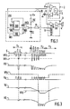
- FIG. 1 represents the general diagram of a device comprising a microphone 1, a signal amplification and processing chain 2 and 3, and a loudspeaker 4.
- the block represented by 2 comprises a preamplifier 5 for the microphone signal, a splitter module 6 also called a hybrid function, connected to the telephone line L and a listening preamplifier 7 for the earpiece 8 of the handset.
- the block shown in 3 amplifies the listening signal in order to power the loudspeaker 4 and includes a preamplifier stage 3a with controllable gain and a power amplifier stage 3b with fixed gain.
- a gain control circuit 10 of the listening amplifier per speaker contained in block 3 is provided.
- the gain control circuit 10 is generally behaves like a feedback loop. Its input signal S can be taken from any point in the amplification chain between the microphone 1 and the loudspeaker 4, but preferably it is taken from the microphone 1, in particular in the case of a telephone set. According to the invention the signal S is applied after a possible amplification at the input of first control means 100 which perform a comparison of the signal S with a first reference voltage VR1.
- the gain control circuit 10 also includes a capacitor C, one armature of which is connected to ground and the other is charged from the positive potential V + through a load resistor RC.
- the charging voltage VC of this capacitor C can be limited if desired by a voltage limiter 11 constituted for example by a number semiconductor junctions live situation which may exist by construction at the gain control input of the preamplifier stage 3a.
- the voltage VC is used for the gain control of the listening amplifier 3 and can be converted into control current by means of a resistor R as shown in the figure.
- the capacitor C can be discharged by the output of the first control means 100 through a first discharge resistor RD1 and a second discharge resistor RD2 connected in series.
- the quiescent voltage of the signal S determines with respect to the first reference voltage VR1 a first threshold which, when it is not crossed, maintains the output of the first control means 100 in the high impedance state, the output of these means being of the open collector type.
- the first threshold is crossed the output of the first control means 100 goes to the low state and causes the discharge of the capacitor C through the discharge resistors RD1 and RD2 according to a first time constant which is equal to (RD1 + RD2 ) .VS .
- the signal S is also applied to the input of second control means 200 and this signal is compared to a second reference voltage VR2 while the output of these second control means 200 is connected to the intermediate point between the discharge resistors RD1 and RD2.
- the second reference voltage VR2 is chosen such that it forms, with the quiescent voltage of the signal S, a second threshold lower than said first threshold.
- the second control means 200 are also controlled from the charging voltage VC of the capacitor C, and the output of these second means is only activated when the voltage VC has dropped below d a third reference voltage VR3 corresponding to the voltage presented by the capacitor C for a reduced gain value which serves as a reference.
- the second control means 200 do not command a reduction in the gain of the power amplifier until the first control means 100 have already reduced the gain below said reference value.
- the output of the second control means 200 which is also of the open collector type causes a discharge of the capacitor C through the discharge resistance RD2 chosen preferably with a value much lower than the first discharge resistance RD1 and therefore according to a second time constant much lower than the first time constant of the first control means 100. If the signal S of the microphone maintains a relatively high amplitude, that is to say greater than the second threshold determined by the second reference voltage VR2 , the gain of the listening amplifier 3 is regulated by the second control means 200.
- Another alternative embodiment concerns the discharge resistors RD1 and RD2 which can be suppressed when the outputs of the control means 100 and 200 operate at a fixed current when they are in their conductive state.
- an output current value of the first control means 100 is then chosen which is preferably much lower than the value of the output current of the second control means 200.
- FIG. 2 shows, by way of example of implementation, a more detailed diagram of the control circuit 10 of FIG. 1.
- the two microphone terminals are connected to the two input terminals 13 and 14 of the control circuit 10.
- the continuous reference of the microphone signal is first eliminated by a pi filter constituted by the series association of the capacitor 15 of the resistor 16 and of the capacitor 17.
- the microphone signal thus filtered is applied via the protection resistors 18 and 19 to the inputs of a differential amplifier 20.
- the main reference voltage VR0 is applied to the positive input of the differential amplifier 20 through a protection resistor 25 and the negative input of this differential amplifier is looped back to its output via a feedback resistor 26.
- the signal which is denoted S 'in the figure and which is the microphone signal amplified by the differential amplifier 20, has a continuous level substantially equal to the main reference voltage VR0.
- the gain of the differential amplifier 20 is established near 50 the reference voltages VR0, VR1 and VR2 are established around half of the voltage V + while the reference voltage VR1 is lower at the main reference voltage VR0 of approximately 12 millivolts, the difference which constitutes said first threshold, and that the second reference voltage VR2 is less than the main reference voltage VR0 by 1.5 millivolt, and constitutes said second threshold which is eight times smaller than the first threshold.
- the signal S ′ coming from the microphone, after amplification, is applied to the positive input of a first comparator 101 with open collector output and the negative input of which receives the first reference voltage VR1.
- the signal S ' is also applied to the negative input of a second comparator 202 with open collector output while its positive input receives the second reference voltage VR2.
- the output of the comparator 202 is connected to the intermediate point A of a bridge constituted by the resistor 28 also connected to the positive voltage V + and by the resistor 29 connected to the ground.
- the values of resistors 28 and 29 are chosen so that the voltage VA of point A is slightly greater than half of the positive voltage V +.
- a third comparator 203 with open collector output has its negative input connected to point A.
- a fourth comparator 204 with open collector output has its negative input brought to a third reference voltage VR3 carried by the intermediate point B of a resistance bridge 30 and 31 which are also connected respectively to the positive voltage V + and to ground.
- the third reference voltage VR3 corresponds to the voltage presented by the capacitor C for a certain value of reference gain below which the second control means must come into action, as will be explained below.
- the capacitor C is permanently charged from the positive voltage V + through the load resistor RC and possibly discharged according to the circumstances from the outputs of the first comparator 101 and of the third comparator 203 through the discharge resistors RD1 and RD2 respectively whose serial connection is connected to the junction point between the load resistor RC and the capacitor C.
- the output of the third comparator 203 which when it is at high impedance carries a voltage substantially equal to the charging voltage of the capacitor C is connected via a protective resistor 32 to the input positive of the fourth comparator 204.
- the output of the fourth comparator 204 is connected to the foot of a bridge made up of resistors 34 and 35 which is connected at the head to the positive voltage V + and the intermediate point F of which shows a fourth reference voltage VR4 which, when the output of the fourth comparator 204 is in the low state, is set to a value lower than the voltage VA of point A when the output of the second comparator 202 is in the high impedance state.
- the intermediate point F of the resistance bridge 34 and 35 is connected to the positive input of the third comparator 203.
- a first period t1 has been shown during which the signal S 'has a temporarily high amplitude which is characteristic of the speech signal.
- the control circuit 10 takes advantage of this characteristic property of the voice signal.
- the first comparator 101 has its output which goes to the low state when the first reference voltage VR1 is crossed and gradually influences through the discharge resistance DR1 of relatively high value, on the charge voltage VC of the capacitor C.
- the second reference voltage VR2 is also crossed so that the second comparator 202 has its output which has a signal VA which at rest is in the low state and has positive slots for the corresponding alternations of the signal S ⁇ however that the fourth comparator 204 not having switched the voltage VR4 of the point F remains at the highest potential V +.
- the third comparator 203 does not switch during this time period t1.
- FIG. 3 also shows another time period t2 during which an acoustic coupling condition is assumed to be achieved such that the system oscillates while for the following time period t3 the oscillation conditions have disappeared.
- a first time interval corresponding to the first discharge time constant due to the action of the first comparator 101 and the first discharge resistance RD1 the gain of the listening amplifier 3 is gradually reduced under the sole effect of the first comparator 101 and this until the charging voltage of the capacitor VC falls below the third reference voltage VR3.
- the fourth comparator 204 switches and the point F shows a reference voltage VR4 lower than the apex of the positive slots of the signal VA at the output of the comparator 202.
- the third comparator 203 is able to switch to response to the positive slots of the output of the second comparator 202 and induces on its output in the low state an accelerated discharge of the capacitor C under the effect of the discharge resistance RD2 chosen much lower than the resistance RD1.
- the gain then quickly goes to a very low value under the effect of the voltage control of the capacitor C and the circuit then regulates the value of this gain according to the conditions and of the amplitude of the signal S 'as long as it has an amplitude such that the second reference voltage VR2 remains crossed by the negative half-waves of this signal.
- the signal S ' is assumed to be reduced to a low value such that neither of the two thresholds is exceeded.
- the outputs of the first comparators 101 and third comparator 203 are now in the high impedance state so that the capacitor C is recharged through the load resistor RC.
- the fourth comparator 204 again switches to the state of high impedance at the output so that the voltage at the point F rises to the value of the positive voltage V +.
- the set of comparators 202, 203 and 204 returns to its stable point of operation in the absence of a high amplitude of the signal S '.
- the comparator 101 playing the role of first control means acts according to a first time constant determined mainly by the discharge resistance RD1 as long as the signal S 'remains of an amplitude which can be regulated by the first means without the gain being lowered below the reference gain corresponding to the third reference voltage VR3.
- the capacitor C discharges according to said first time constant after which all of the comparators 202, 203 and 204 enter into operation with a time constant due to the discharge resistance RD2 which can be chosen for example 20 times lower than the discharge resistance RD1 and this set of comparators constituting the second control means, then regulate the discharge of the capacitor and therefore the gain of the listening amplifier 3 as long as the signal S 'maintains an amplitude which exceeds the second threshold corresponding to the second reference voltage VR2.
- the part of the circuit 10 in FIG. 2, which is surrounded by a dashed frame 36, can be easily integrated in the form of a monolithic circuit.
- certain high value resistors can advantageously be replaced by functionally equivalent elements.
- the first impedance bridge described as being constituted by resistors 28 and 29 can be, according to a variant not shown in the figure, constituted by the association in series of a current source connected to the voltage V + and d a non-linear impedance connected to ground, this non-linear impedance being formed of a plurality of semiconductor junctions in series which normally fixes the voltage VA of point A.
- resistor 21 can be replaced by a current source and resistor 24 by a series of direct semiconductor junctions, while resistors 22 and 23, which are of lower value, can be kept.
Claims (6)
- Verstärkungsregelschaltung (10) eines Verstärkers zum Hören über einen Lautsprecher in einem Gerät, das außerdem ein Mikrophon (1) und einen zugeordneten Verstärker (5) aufweist, insbesondere zum Unterdrücken des Larsen-Effektes, wobei diese Schaltung im wesentlichen eine Gegenkopplungsschleife bildet, welche die Verstärkung des Verstärkers (3) zum Hören über den Lautsprecher verringert, wenn das von dem Mikrophon herrührende Signal eine vorbestimmte Schwelle überschreitet, dadurch gekennzeichnet, daß die Gegenkopplungsschleife, die erste Regelmittel (100) aufweist, die eine Verringerung der Verstärkung zum Hören über den Lautsprecher mit einer ersten Zeitkonstanten regeln und daß die genannte vorbestimmte Schwelle eine erste Schwelle (VR1) ist, und daß die Schleife außerdem zweite Regelmittel aufweist, die das Mikrophonsignal mit einer zweiten Schwelle (VR2) vergleichen, die niedriger ist als die genannte erste Schwelle, wobei diese Mittel eine Verringerung der Verstärkung mit einer gegenüber der ersten, niedrigeren zweiten Zeitkonstanten herbeiführen, ausgehend von dem Zeitpunkt, an dem die Verstärkung durch die genannten ersten Mittel bis unter einen Bezugsverstärkungswert zurückgebracht wird, während sie inaktiv bleiben, wenn die Verstärkung höher bleibt als der genannte Bezugswert.
- Verstärkungsregelschaltung nach Anspruch 1, dadurch gekennzeichnet, daß die Verstärkung des Verstärkers zum Hören über den Lautsprecher durch die Ladespannung (VC) eines über eine Stromquelle konstant geladenen Kondensators gesteuert wird, und daß die ersten und zweiten Regelmittel mit ihrem die Entladung des Kondensators herbeiführenden Ausgang über einen ersten (RD1) bzw. einen zweiten Entladewiderstand (RD2) verbunden sind, wobei der erste Entladewiderstand einen Wert aufweist, der höher ist als der des zweiten Entladewiderstandes.
- Verstärkungsregelschaltung nach Anspruch 2, dadurch gekennzeichnet, daß der Kondensator aus dem positivsten Potential der Schaltung aufgeladen wird, daß die genannten ersten und zweiten Regelmittel (100, 200) über ihren Ausgang, der vom Typ eines NPN-Transistors ist (oder vom N-Kanal MOS-Typ) mit offenem Kollektor (oder mit offener Drain), den Kondensator entladen, und daß der erste Entladewiderstand (RD1) des Kondensators mit dem zweiten Entladewiderstand (RD2) reihengeschaltet ist.
- Verstärkungsregelschaltung nach Anspruch 1, dadurch gekennzeichnet, daß die Verstärkung des Verstärkers zum Hören über den Lautsprecher durch die Ladespannung (VC) eines Kondensators gesteuert wird, der über eine Stromquelle konstant aufgeladen wird, und daß die ersten und zweiten Regelmittel (100, 200) die Entladung dieses Kondensators mittels eines Stromes herbeiführen, dessen Wert an dem Ausgang jedes dieser Regelmittel vorbestimmt wird, wobei der Ausgangsstrom der ersten Mittel auf einen Wert festgesetzt wird, der niedriger ist als der Wert des Ausgangsstromes der zweiten Mittel, und wobei die betreffenden Ausgänge mit dem Kondensator parallelgeschaltet sind.
- Verstärkungsregelschaltung nach Anspruch 3 oder 4, dadurch gekennzeichnet, daß die ersten Regelmittel eine erste Vergleichsschaltung (101) aufweisen, deren positiver Eingang das von dem Mikrophon herrührende, verstärkte Signal (5) erhält, deren negativer Eingang auf einer erste Bezugsspannung (VR1) gebracht wird, die niedriger ist als der kontinuierliche Pegel des Mikrophonsignals und die genannte erste Schwelle gegenüber diesem Pegel bestimmt, und deren Ausgang (VD) den Ausgang der genannten Regelmittel bildet, daß die zweiten Regelmittel eine zweite, eine dritte und eine vierte Vergleichsschaltung (202, 203, 204) aufweisen, alle mit einem Ausgang vom Typ eines NPN-Transistors mit offenem Kollektor, daß die zweite Vergleichsschaltung einen negativen Eingang aufweist, der das verstärkte Mikrophonsignal (5') erhält, und einen positiven Eingang, der auf eine zweite Bezugsspannung (VR2) gebracht wird, die etwas höher ist als die erste Bezugsspannung, aber niedriger als der kontinuierliche Pegel des Mikrophonsignals und gegenüber diesem Pegel die zweite Schwelle bestimmt, daß der Ausgang der zweiten Vergleichsschaltung (202) einerseits mit dem Mittenabgriff einer ersten Impedanzbrücke verbunden ist, die u.a. zwischen den äußersten Spannungen der Schaltung verbunden ist, und andererseits mit dem negativen Eingang der dritten Vergleichsschaltung (203) verbunden ist, daß die vierte Vergleichsschaltung (204) an dem positiven Eingang eine Spannung erhält, die der Ladespannung des Kondensators nahezu entspricht und an dem negativen Eingang, der auf eine dritte Bezugsspannung gebracht ist, die der Spannung entspricht, die durch den Kondensator für den genannten Bezugsverstärkungswert angeboten wird, daß der Ausgang der vierten Vergleichsschaltung mit dem Schenkel einer zweiten Impedanzbrücke verbunden ist, deren Kopf mit der positiveren Spannung verbunden ist, und deren Mittenabgriff mit dem negativen Eingang der dritten Vergleichsschaltung verbunden ist und eine vierte Bezugsspannung erscheinen läßt, wenn der Ausgang der vierten Vergleichsschaltung niedrig ist, wobei diese vierte Bezugsspannung auf einen Wert geregelt wird, der niedriger ist als die Spannung des Mittenabgriffs der ersten Impedanzbrücke, wenn der Ausgang der zweiten Vergleichsschaltung sich in dem Zustand hoher Impedanz befindet, und daß der Ausgang der dritten Vergleichsschaltung den Ausgang der genannten zweiten Regelmittel bildet.
- Verwendung der Regelschaltung nach einem der Ansprüche 1 bis 5 bei einem lautsprechenden Fernsprechapparat.
Applications Claiming Priority (2)
| Application Number | Priority Date | Filing Date | Title |
|---|---|---|---|
| FR8702660 | 1987-02-27 | ||
| FR8702660A FR2611408B1 (fr) | 1987-02-27 | 1987-02-27 | Circuit de commande d e gain d'un amplificateur d'ecoute par haut-parleur pour la suppression de l'effet larsen |
Publications (2)
| Publication Number | Publication Date |
|---|---|
| EP0280381A1 EP0280381A1 (de) | 1988-08-31 |
| EP0280381B1 true EP0280381B1 (de) | 1992-01-15 |
Family
ID=9348420
Family Applications (1)
| Application Number | Title | Priority Date | Filing Date |
|---|---|---|---|
| EP88200355A Expired - Lifetime EP0280381B1 (de) | 1987-02-27 | 1988-02-25 | Anti-Larsen-Pegelregelungsanordnung in einem Verstärker eines Fernsprechapparats |
Country Status (6)
| Country | Link |
|---|---|
| US (1) | US4835484A (de) |
| EP (1) | EP0280381B1 (de) |
| JP (1) | JPH0716216B2 (de) |
| KR (1) | KR960011067B1 (de) |
| DE (1) | DE3867654D1 (de) |
| FR (1) | FR2611408B1 (de) |
Families Citing this family (7)
| Publication number | Priority date | Publication date | Assignee | Title |
|---|---|---|---|---|
| US5369711A (en) * | 1990-08-31 | 1994-11-29 | Bellsouth Corporation | Automatic gain control for a headset |
| US5371803A (en) * | 1990-08-31 | 1994-12-06 | Bellsouth Corporation | Tone reduction circuit for headsets |
| JP3058923B2 (ja) * | 1991-01-11 | 2000-07-04 | 株式会社東芝 | 無線電話装置アダプタ |
| JPH04239251A (ja) * | 1991-01-11 | 1992-08-27 | Toshiba Corp | 無線電話装置アダプタ |
| EP0494780B1 (de) * | 1991-01-11 | 1997-03-26 | Kabushiki Kaisha Toshiba | Adapter zur Versorgung eines transportablen Funktelefons mit Spannung |
| US5701352A (en) * | 1994-07-14 | 1997-12-23 | Bellsouth Corporation | Tone suppression automatic gain control for a headset |
| US11589154B1 (en) * | 2021-08-25 | 2023-02-21 | Bose Corporation | Wearable audio device zero-crossing based parasitic oscillation detection |
Family Cites Families (6)
| Publication number | Priority date | Publication date | Assignee | Title |
|---|---|---|---|---|
| US4346261A (en) * | 1980-03-17 | 1982-08-24 | United Networks, Inc. | Speaker phones |
| CA1186826A (en) * | 1981-03-18 | 1985-05-07 | Jin H. Yun | Loudspeaker telephone system |
| DE3148305A1 (de) * | 1981-12-03 | 1983-06-09 | Deutsche Telephonwerke Und Kabelindustrie Ag, 1000 Berlin | Schaltungsanordnung fuer eine freisprecheinrichtung |
| FR2518854B1 (fr) * | 1981-12-18 | 1986-08-08 | Thomson Csf Mat Tel | Poste telephonique a amplificateurs de parole |
| FR2537810A1 (fr) * | 1982-12-14 | 1984-06-15 | Thomson Csf | Poste telephonique a ecoute amplifiee muni d'un dispositif antilarsen |
| US4542263A (en) * | 1984-03-07 | 1985-09-17 | Oki Electric Industry Co., Ltd. | Speech control circuit |
-
1987
- 1987-02-27 FR FR8702660A patent/FR2611408B1/fr not_active Expired
-
1988
- 1988-02-18 US US07/161,565 patent/US4835484A/en not_active Expired - Lifetime
- 1988-02-24 KR KR1019880001894A patent/KR960011067B1/ko not_active IP Right Cessation
- 1988-02-24 JP JP63039746A patent/JPH0716216B2/ja not_active Expired - Lifetime
- 1988-02-25 DE DE8888200355T patent/DE3867654D1/de not_active Expired - Lifetime
- 1988-02-25 EP EP88200355A patent/EP0280381B1/de not_active Expired - Lifetime
Also Published As
| Publication number | Publication date |
|---|---|
| KR880010566A (ko) | 1988-10-10 |
| FR2611408B1 (fr) | 1989-05-26 |
| EP0280381A1 (de) | 1988-08-31 |
| DE3867654D1 (de) | 1992-02-27 |
| JPS63227242A (ja) | 1988-09-21 |
| KR960011067B1 (ko) | 1996-08-16 |
| JPH0716216B2 (ja) | 1995-02-22 |
| FR2611408A1 (fr) | 1988-09-02 |
| US4835484A (en) | 1989-05-30 |
Similar Documents
| Publication | Publication Date | Title |
|---|---|---|
| EP0280381B1 (de) | Anti-Larsen-Pegelregelungsanordnung in einem Verstärker eines Fernsprechapparats | |
| FR2724072A1 (fr) | Etage amplificateur de puissance, de type suiveur. | |
| FR2484740A1 (fr) | Circuit de protection pour un transistor de commutation et son procede de realisation | |
| EP0271938B1 (de) | Automatische Verstärkungsregelung einer Verstärkerschaltung | |
| EP0649079B1 (de) | Geregelter Spannungsquellengenerator der Bandgapbauart | |
| FR2853471A1 (fr) | Circuit amplificateur audio | |
| EP0022015B1 (de) | Audioverstärker und Verfahren zur Audiofrequenzverstärkung | |
| EP0377205B1 (de) | Strombegrenzer und seine Verwendung in einem optischen Empfänger | |
| FR3025373A1 (de) | ||
| EP0415503B1 (de) | Integrierte Schaltung mit einer Feststellung des Sättigungszustandes | |
| FR2524732A1 (fr) | Circuit de protection contre les surcharges | |
| FR3069397A1 (fr) | Circuit et procede de pilotage d'un amplificateur audio | |
| FR2635680A1 (fr) | Prothese auditive | |
| FR2460576A1 (fr) | Circuit d'alimentation a trois bornes pour appareil telephonique | |
| FR2611283A1 (fr) | Dispositif comportant un circuit electronique de traitement d'un signal analogique | |
| FR2946202A1 (fr) | Annulation de glitche pour amplificateur audio | |
| EP0305301B1 (de) | Signalkompressorschaltung, insbesondere für Fernsprechapparate | |
| WO1994030005A1 (fr) | Dispositif d'extraction de synchronisation d'un signal video | |
| EP0065335B1 (de) | Einrichtung zur Vermeidung störender ungedämpfter Schwingungen in einem Schleifensystem und diese Einrichtung verwendender Fernsprechapparat mit Lautsprecher | |
| FR2645373A1 (fr) | Procede et dispositif de reduction du bruit sur un signal codable a plusieurs niveaux predetermines | |
| FR2853472A1 (fr) | Circuit amplificateur audio | |
| EP0847193A1 (de) | Zwischenfrequenzverstärker für Funkwellenempfänger | |
| EP0836272B1 (de) | Rauscharme Verstärkungsanordnung | |
| FR2674705A1 (fr) | Dispositif amplificateur video. | |
| FR3103333A1 (fr) | Dispositif pour générer un courant |
Legal Events
| Date | Code | Title | Description |
|---|---|---|---|
| PUAI | Public reference made under article 153(3) epc to a published international application that has entered the european phase |
Free format text: ORIGINAL CODE: 0009012 |
|
| AK | Designated contracting states |
Kind code of ref document: A1 Designated state(s): DE FR GB IT SE |
|
| 17P | Request for examination filed |
Effective date: 19890209 |
|
| RAP1 | Party data changed (applicant data changed or rights of an application transferred) |
Owner name: N.V. PHILIPS' GLOEILAMPENFABRIEKEN Owner name: PHILIPS COMPOSANTS |
|
| 17Q | First examination report despatched |
Effective date: 19910313 |
|
| GRAA | (expected) grant |
Free format text: ORIGINAL CODE: 0009210 |
|
| AK | Designated contracting states |
Kind code of ref document: B1 Designated state(s): DE FR GB IT SE |
|
| REF | Corresponds to: |
Ref document number: 3867654 Country of ref document: DE Date of ref document: 19920227 |
|
| ITF | It: translation for a ep patent filed |
Owner name: ING. C. GREGORJ S.P.A. |
|
| GBT | Gb: translation of ep patent filed (gb section 77(6)(a)/1977) | ||
| PLBE | No opposition filed within time limit |
Free format text: ORIGINAL CODE: 0009261 |
|
| STAA | Information on the status of an ep patent application or granted ep patent |
Free format text: STATUS: NO OPPOSITION FILED WITHIN TIME LIMIT |
|
| 26N | No opposition filed | ||
| EAL | Se: european patent in force in sweden |
Ref document number: 88200355.1 |
|
| ITPR | It: changes in ownership of a european patent |
Owner name: CAMBIO RAGIONE SOCIALE;PHILIPS ELECTRONICS N.V. |
|
| REG | Reference to a national code |
Ref country code: FR Ref legal event code: CD |
|
| REG | Reference to a national code |
Ref country code: FR Ref legal event code: TP |
|
| PGFP | Annual fee paid to national office [announced via postgrant information from national office to epo] |
Ref country code: FR Payment date: 20010216 Year of fee payment: 14 |
|
| PGFP | Annual fee paid to national office [announced via postgrant information from national office to epo] |
Ref country code: SE Payment date: 20010223 Year of fee payment: 14 |
|
| PGFP | Annual fee paid to national office [announced via postgrant information from national office to epo] |
Ref country code: GB Payment date: 20010227 Year of fee payment: 14 |
|
| PGFP | Annual fee paid to national office [announced via postgrant information from national office to epo] |
Ref country code: DE Payment date: 20010420 Year of fee payment: 14 |
|
| REG | Reference to a national code |
Ref country code: GB Ref legal event code: IF02 |
|
| PG25 | Lapsed in a contracting state [announced via postgrant information from national office to epo] |
Ref country code: GB Free format text: LAPSE BECAUSE OF NON-PAYMENT OF DUE FEES Effective date: 20020225 |
|
| PG25 | Lapsed in a contracting state [announced via postgrant information from national office to epo] |
Ref country code: SE Free format text: LAPSE BECAUSE OF NON-PAYMENT OF DUE FEES Effective date: 20020226 |
|
| PG25 | Lapsed in a contracting state [announced via postgrant information from national office to epo] |
Ref country code: DE Free format text: LAPSE BECAUSE OF NON-PAYMENT OF DUE FEES Effective date: 20020903 |
|
| EUG | Se: european patent has lapsed |
Ref document number: 88200355.1 |
|
| GBPC | Gb: european patent ceased through non-payment of renewal fee |
Effective date: 20020225 |
|
| PG25 | Lapsed in a contracting state [announced via postgrant information from national office to epo] |
Ref country code: FR Free format text: LAPSE BECAUSE OF NON-PAYMENT OF DUE FEES Effective date: 20021031 |
|
| REG | Reference to a national code |
Ref country code: FR Ref legal event code: ST |
|
| PG25 | Lapsed in a contracting state [announced via postgrant information from national office to epo] |
Ref country code: IT Free format text: LAPSE BECAUSE OF NON-PAYMENT OF DUE FEES;WARNING: LAPSES OF ITALIAN PATENTS WITH EFFECTIVE DATE BEFORE 2007 MAY HAVE OCCURRED AT ANY TIME BEFORE 2007. THE CORRECT EFFECTIVE DATE MAY BE DIFFERENT FROM THE ONE RECORDED. Effective date: 20050225 |