EP0280381B1 - Anti-larsen effect gain control circuit in a telephone amplifier - Google Patents
Anti-larsen effect gain control circuit in a telephone amplifier Download PDFInfo
- Publication number
- EP0280381B1 EP0280381B1 EP88200355A EP88200355A EP0280381B1 EP 0280381 B1 EP0280381 B1 EP 0280381B1 EP 88200355 A EP88200355 A EP 88200355A EP 88200355 A EP88200355 A EP 88200355A EP 0280381 B1 EP0280381 B1 EP 0280381B1
- Authority
- EP
- European Patent Office
- Prior art keywords
- gain
- control means
- output
- comparator
- capacitor
- Prior art date
- Legal status (The legal status is an assumption and is not a legal conclusion. Google has not performed a legal analysis and makes no representation as to the accuracy of the status listed.)
- Expired - Lifetime
Links
Images

Classifications
-
- H—ELECTRICITY
- H03—ELECTRONIC CIRCUITRY
- H03G—CONTROL OF AMPLIFICATION
- H03G3/00—Gain control in amplifiers or frequency changers without distortion of the input signal
- H03G3/20—Automatic control
- H03G3/30—Automatic control in amplifiers having semiconductor devices
-
- H—ELECTRICITY
- H03—ELECTRONIC CIRCUITRY
- H03G—CONTROL OF AMPLIFICATION
- H03G1/00—Details of arrangements for controlling amplification
- H03G1/0005—Circuits characterised by the type of controlling devices operated by a controlling current or voltage signal
- H03G1/0088—Circuits characterised by the type of controlling devices operated by a controlling current or voltage signal using discontinuously variable devices, e.g. switch-operated
-
- H—ELECTRICITY
- H04—ELECTRIC COMMUNICATION TECHNIQUE
- H04M—TELEPHONIC COMMUNICATION
- H04M9/00—Arrangements for interconnection not involving centralised switching
- H04M9/08—Two-way loud-speaking telephone systems with means for conditioning the signal, e.g. for suppressing echoes for one or both directions of traffic
Definitions
- the present invention relates to a gain control circuit of an amplifier for listening by loudspeaker in a device also comprising a microphone and its associated amplifier, in particular for the purpose of eliminating the Larsen effect, a circuit consisting essentially of a feedback loop reducing the gain of the loudspeaker amplifier when the signal from the microphone exceeds a determined threshold.
- the invention also relates to the application of this gain control circuit to a telephone set with amplified listening by loudspeaker. It is well known that in all systems comprising both a speaker powered by its amplifier and a microphone whose signal is applied more or less directly to the amplifier, there is a risk of oscillation by Larsen effect. due to the acoustic coupling between the speaker and the microphone. This is the case for example of a telephone set provided with an amplified listening, case to which the invention is addressed more particularly but not exclusively.
- the Larsen effect detection circuit must be very selective to distinguish an oscillation signal from an audio signal. high amplitude but momentary like an ambient noise or a shock on the microphone.
- the invention aims to provide a suitable control circuit for the gain of the loudspeaker amplifier, avoiding relaxation and which would use essentially integrable circuits.
- control circuit in accordance with the preliminary paragraph, characterized in that the feedback loop comprising first control means, controlling a gain reduction of the listening amplifier by loudspeaker with a first time constant, and said predetermined threshold being a first threshold, it also comprises second control means comparing the signal coming from the microphone with a second threshold, lower than said first threshold, which control a reduction in gain with a second time constant lower than the first, from the moment when the gain has been reduced below a reference gain value by said first means, while they remain inactive when the gain remains greater than said reference value.
- said first control means are normally sufficient to properly attenuate the amplification of the listening signal by loudspeaker, if necessary, and to regulate the amplification of the usual way.
- any acoustic signal which arrives at the microphone with a high level but for a short duration, that is to say a duration less than the first time constant, does not trigger the second means, in contrast to the instability caused by the 'Larsen effect which generates, by acoustic coupling, a strong microphone signal and for a generally long duration depending on the acoustic coupling conditions between the loudspeaker and the microphone.
- the first control means have led to lowering the gain below the determined value taken as a reference, which occurs after the first time constant
- the second control means come into action with a time constant set significantly more lower than the time constant of the first means, and the gain is quickly reduced to the value necessary for the regulation to operate by comparison with the second threshold.
- the second threshold is chosen to be lower than the first threshold, relaxation does not occur and the circuit returns to normal gain conditions only when the microphone signal drops below the second threshold, i.e. in practice when the cause of the oscillation has disappeared.
- the gain control circuit is characterized in that the gain of the loudspeaker amplifier is controlled by the charging voltage of a capacitor, permanently charged through a current source and in that the first and second control means have their outputs which cause the discharge of this capacitor via respectively a first and a second discharge resistance, the first discharge resistance having a higher value than that of the second discharge resistor.
- control circuit is further characterized in that the capacitor is charged from the most positive potential of the circuit, in that said first and second control means discharge the capacitor by their terminal.
- output which is of the NPN transistor type (or N channel MOS), with open collector (or open drain), and in that the first discharge resistance of the capacitor is arranged in series with the second discharge resistance.
- Transistors of this type have the advantage of being easily integrated.
- open collector type outputs makes it possible to couple the outputs of the first and second control means through their respective discharge resistance since the high impedance state of the output of one of the control means remains without effect on the output of the other.
- a variant of this embodiment dispenses with the use of discharge resistors when the first and second control means have their output which operates at a discharge current limited to a fixed value; the output current of the first means is then fixed at a lower value than the value of the output current of the second means, and the outputs in question are connected in parallel on the capacitor.
- a particular embodiment of the invention is characterized in that the first control means comprise a first comparator whose positive input receives the signal from the microphone after amplification, whose negative input is brought to a first voltage reference which being lower than the continuous level of the signal from the microphone, defines with respect to this level said first threshold, and the output of which constitutes the output of said first control means, in that the second control means comprise a second, a third and fourth comparator, all with open collector type output of an NPN transistor, in that the second comparator has its negative input which receives the signal from the microphone after amplification, and its positive input which is brought to a second reference voltage slightly higher than the first reference voltage but nevertheless lower than the continuous level of the signal coming from the microphone and which defines with respect to this level said second threshold, in that the output of the second comparator is on the one hand connected to the intermediate point of a first impedance bridge which is also connected between the extreme voltages of the circuit and on the other hand connected to the negative input of the third comparator, in that the fourth comparator receives on its positive
- the elements constituting the control circuit can be integrated, which leads to a particularly economical circuit.
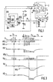
- FIG. 1 represents the general diagram of a device comprising a microphone 1, a signal amplification and processing chain 2 and 3, and a loudspeaker 4.
- the block represented by 2 comprises a preamplifier 5 for the microphone signal, a splitter module 6 also called a hybrid function, connected to the telephone line L and a listening preamplifier 7 for the earpiece 8 of the handset.
- the block shown in 3 amplifies the listening signal in order to power the loudspeaker 4 and includes a preamplifier stage 3a with controllable gain and a power amplifier stage 3b with fixed gain.
- a gain control circuit 10 of the listening amplifier per speaker contained in block 3 is provided.
- the gain control circuit 10 is generally behaves like a feedback loop. Its input signal S can be taken from any point in the amplification chain between the microphone 1 and the loudspeaker 4, but preferably it is taken from the microphone 1, in particular in the case of a telephone set. According to the invention the signal S is applied after a possible amplification at the input of first control means 100 which perform a comparison of the signal S with a first reference voltage VR1.
- the gain control circuit 10 also includes a capacitor C, one armature of which is connected to ground and the other is charged from the positive potential V + through a load resistor RC.
- the charging voltage VC of this capacitor C can be limited if desired by a voltage limiter 11 constituted for example by a number semiconductor junctions live situation which may exist by construction at the gain control input of the preamplifier stage 3a.
- the voltage VC is used for the gain control of the listening amplifier 3 and can be converted into control current by means of a resistor R as shown in the figure.
- the capacitor C can be discharged by the output of the first control means 100 through a first discharge resistor RD1 and a second discharge resistor RD2 connected in series.
- the quiescent voltage of the signal S determines with respect to the first reference voltage VR1 a first threshold which, when it is not crossed, maintains the output of the first control means 100 in the high impedance state, the output of these means being of the open collector type.
- the first threshold is crossed the output of the first control means 100 goes to the low state and causes the discharge of the capacitor C through the discharge resistors RD1 and RD2 according to a first time constant which is equal to (RD1 + RD2 ) .VS .
- the signal S is also applied to the input of second control means 200 and this signal is compared to a second reference voltage VR2 while the output of these second control means 200 is connected to the intermediate point between the discharge resistors RD1 and RD2.
- the second reference voltage VR2 is chosen such that it forms, with the quiescent voltage of the signal S, a second threshold lower than said first threshold.
- the second control means 200 are also controlled from the charging voltage VC of the capacitor C, and the output of these second means is only activated when the voltage VC has dropped below d a third reference voltage VR3 corresponding to the voltage presented by the capacitor C for a reduced gain value which serves as a reference.
- the second control means 200 do not command a reduction in the gain of the power amplifier until the first control means 100 have already reduced the gain below said reference value.
- the output of the second control means 200 which is also of the open collector type causes a discharge of the capacitor C through the discharge resistance RD2 chosen preferably with a value much lower than the first discharge resistance RD1 and therefore according to a second time constant much lower than the first time constant of the first control means 100. If the signal S of the microphone maintains a relatively high amplitude, that is to say greater than the second threshold determined by the second reference voltage VR2 , the gain of the listening amplifier 3 is regulated by the second control means 200.
- Another alternative embodiment concerns the discharge resistors RD1 and RD2 which can be suppressed when the outputs of the control means 100 and 200 operate at a fixed current when they are in their conductive state.
- an output current value of the first control means 100 is then chosen which is preferably much lower than the value of the output current of the second control means 200.
- FIG. 2 shows, by way of example of implementation, a more detailed diagram of the control circuit 10 of FIG. 1.
- the two microphone terminals are connected to the two input terminals 13 and 14 of the control circuit 10.
- the continuous reference of the microphone signal is first eliminated by a pi filter constituted by the series association of the capacitor 15 of the resistor 16 and of the capacitor 17.
- the microphone signal thus filtered is applied via the protection resistors 18 and 19 to the inputs of a differential amplifier 20.
- the main reference voltage VR0 is applied to the positive input of the differential amplifier 20 through a protection resistor 25 and the negative input of this differential amplifier is looped back to its output via a feedback resistor 26.
- the signal which is denoted S 'in the figure and which is the microphone signal amplified by the differential amplifier 20, has a continuous level substantially equal to the main reference voltage VR0.
- the gain of the differential amplifier 20 is established near 50 the reference voltages VR0, VR1 and VR2 are established around half of the voltage V + while the reference voltage VR1 is lower at the main reference voltage VR0 of approximately 12 millivolts, the difference which constitutes said first threshold, and that the second reference voltage VR2 is less than the main reference voltage VR0 by 1.5 millivolt, and constitutes said second threshold which is eight times smaller than the first threshold.
- the signal S ′ coming from the microphone, after amplification, is applied to the positive input of a first comparator 101 with open collector output and the negative input of which receives the first reference voltage VR1.
- the signal S ' is also applied to the negative input of a second comparator 202 with open collector output while its positive input receives the second reference voltage VR2.
- the output of the comparator 202 is connected to the intermediate point A of a bridge constituted by the resistor 28 also connected to the positive voltage V + and by the resistor 29 connected to the ground.
- the values of resistors 28 and 29 are chosen so that the voltage VA of point A is slightly greater than half of the positive voltage V +.
- a third comparator 203 with open collector output has its negative input connected to point A.
- a fourth comparator 204 with open collector output has its negative input brought to a third reference voltage VR3 carried by the intermediate point B of a resistance bridge 30 and 31 which are also connected respectively to the positive voltage V + and to ground.
- the third reference voltage VR3 corresponds to the voltage presented by the capacitor C for a certain value of reference gain below which the second control means must come into action, as will be explained below.
- the capacitor C is permanently charged from the positive voltage V + through the load resistor RC and possibly discharged according to the circumstances from the outputs of the first comparator 101 and of the third comparator 203 through the discharge resistors RD1 and RD2 respectively whose serial connection is connected to the junction point between the load resistor RC and the capacitor C.
- the output of the third comparator 203 which when it is at high impedance carries a voltage substantially equal to the charging voltage of the capacitor C is connected via a protective resistor 32 to the input positive of the fourth comparator 204.
- the output of the fourth comparator 204 is connected to the foot of a bridge made up of resistors 34 and 35 which is connected at the head to the positive voltage V + and the intermediate point F of which shows a fourth reference voltage VR4 which, when the output of the fourth comparator 204 is in the low state, is set to a value lower than the voltage VA of point A when the output of the second comparator 202 is in the high impedance state.
- the intermediate point F of the resistance bridge 34 and 35 is connected to the positive input of the third comparator 203.
- a first period t1 has been shown during which the signal S 'has a temporarily high amplitude which is characteristic of the speech signal.
- the control circuit 10 takes advantage of this characteristic property of the voice signal.
- the first comparator 101 has its output which goes to the low state when the first reference voltage VR1 is crossed and gradually influences through the discharge resistance DR1 of relatively high value, on the charge voltage VC of the capacitor C.
- the second reference voltage VR2 is also crossed so that the second comparator 202 has its output which has a signal VA which at rest is in the low state and has positive slots for the corresponding alternations of the signal S ⁇ however that the fourth comparator 204 not having switched the voltage VR4 of the point F remains at the highest potential V +.
- the third comparator 203 does not switch during this time period t1.
- FIG. 3 also shows another time period t2 during which an acoustic coupling condition is assumed to be achieved such that the system oscillates while for the following time period t3 the oscillation conditions have disappeared.
- a first time interval corresponding to the first discharge time constant due to the action of the first comparator 101 and the first discharge resistance RD1 the gain of the listening amplifier 3 is gradually reduced under the sole effect of the first comparator 101 and this until the charging voltage of the capacitor VC falls below the third reference voltage VR3.
- the fourth comparator 204 switches and the point F shows a reference voltage VR4 lower than the apex of the positive slots of the signal VA at the output of the comparator 202.
- the third comparator 203 is able to switch to response to the positive slots of the output of the second comparator 202 and induces on its output in the low state an accelerated discharge of the capacitor C under the effect of the discharge resistance RD2 chosen much lower than the resistance RD1.
- the gain then quickly goes to a very low value under the effect of the voltage control of the capacitor C and the circuit then regulates the value of this gain according to the conditions and of the amplitude of the signal S 'as long as it has an amplitude such that the second reference voltage VR2 remains crossed by the negative half-waves of this signal.
- the signal S ' is assumed to be reduced to a low value such that neither of the two thresholds is exceeded.
- the outputs of the first comparators 101 and third comparator 203 are now in the high impedance state so that the capacitor C is recharged through the load resistor RC.
- the fourth comparator 204 again switches to the state of high impedance at the output so that the voltage at the point F rises to the value of the positive voltage V +.
- the set of comparators 202, 203 and 204 returns to its stable point of operation in the absence of a high amplitude of the signal S '.
- the comparator 101 playing the role of first control means acts according to a first time constant determined mainly by the discharge resistance RD1 as long as the signal S 'remains of an amplitude which can be regulated by the first means without the gain being lowered below the reference gain corresponding to the third reference voltage VR3.
- the capacitor C discharges according to said first time constant after which all of the comparators 202, 203 and 204 enter into operation with a time constant due to the discharge resistance RD2 which can be chosen for example 20 times lower than the discharge resistance RD1 and this set of comparators constituting the second control means, then regulate the discharge of the capacitor and therefore the gain of the listening amplifier 3 as long as the signal S 'maintains an amplitude which exceeds the second threshold corresponding to the second reference voltage VR2.
- the part of the circuit 10 in FIG. 2, which is surrounded by a dashed frame 36, can be easily integrated in the form of a monolithic circuit.
- certain high value resistors can advantageously be replaced by functionally equivalent elements.
- the first impedance bridge described as being constituted by resistors 28 and 29 can be, according to a variant not shown in the figure, constituted by the association in series of a current source connected to the voltage V + and d a non-linear impedance connected to ground, this non-linear impedance being formed of a plurality of semiconductor junctions in series which normally fixes the voltage VA of point A.
- resistor 21 can be replaced by a current source and resistor 24 by a series of direct semiconductor junctions, while resistors 22 and 23, which are of lower value, can be kept.
Landscapes
- Engineering & Computer Science (AREA)
- Signal Processing (AREA)
- Control Of Amplification And Gain Control (AREA)
- Amplifiers (AREA)
Description
La présente invention concerne un circuit de commande de gain d'un amplificateur pour l'écoute par haut-parleur dans un appareil comportant par ailleurs un microphone et son amplificateur associé, notamment dans le but de supprimer l'effet Larsen, circuit consistant essentiellement en une boucle de contre-réaction réduisant le gain de l'amplificateur d'écoute par haut-parleur lorsque le signal provenant du microphone dépasse un seuil déterminé.The present invention relates to a gain control circuit of an amplifier for listening by loudspeaker in a device also comprising a microphone and its associated amplifier, in particular for the purpose of eliminating the Larsen effect, a circuit consisting essentially of a feedback loop reducing the gain of the loudspeaker amplifier when the signal from the microphone exceeds a determined threshold.
L'invention concerne également l'application de ce circuit de commande de gain à un poste téléphonique à écoute amplifiée par haut-parleur. Il est bien connu que dans tous les systèmes comportant à la fois un haut-parleur alimenté par son amplificateur ainsi qu'un microphone dont le signal est appliqué plus ou moins directement à l'amplificateur, il existe un risque d'oscillation par effet Larsen dû au couplage acoustique entre le haut-parleur et le microphone. C'est le cas par exemple d'un poste téléphonique muni d'une écoute amplifiée, cas auquel l'invention s'adresse plus particulièrement mais non exclusivement.The invention also relates to the application of this gain control circuit to a telephone set with amplified listening by loudspeaker. It is well known that in all systems comprising both a speaker powered by its amplifier and a microphone whose signal is applied more or less directly to the amplifier, there is a risk of oscillation by Larsen effect. due to the acoustic coupling between the speaker and the microphone. This is the case for example of a telephone set provided with an amplified listening, case to which the invention is addressed more particularly but not exclusively.
Dans un poste téléphonique à écoute amplifiée il est nécessaire de prévoir des moyens pour supprimer l'état d'oscillation Larsen et il est très souhaitable que cette suppression, par une forte réduction du gain de l'amplificateur du haut-parleur, interviennent de manière automatique, c'est-à-dire sans que l'utilisateur du poste ait à exercer une intervention quelconque.In an amplified listening telephone set, it is necessary to provide means to suppress the Larsen state of oscillation and it is very desirable that this suppression, by a strong reduction in the gain of the amplifier of the loudspeaker, intervene so automatic, that is to say without the user of the station having to exert any intervention.
Diverses solutions techniques ont déjà été proposées. D'une manière générale, on peut constater que ces solutions consistent à prévoir, d'une part, un circuit de détection de l'état d'oscillation due à l'effet Larsen fournissant à la sortie un signal de commande qui peut être du type tout ou rien, ou proportionnel, et d'autre part, un circuit de commande proprement dit qui agit sur un étage préamplificateur à gain variable et provoque une réduction, voire une annulation totale du gain lorsque le circuit de détection de l'effet Larsen a constaté un état d'oscillation.Various technical solutions have already been proposed. In general, it can be seen that these solutions consist in providing, on the one hand, a circuit for detecting the state of oscillation due to the Larsen effect providing the output with a control signal which may be of the type all or nothing, or proportional, and on the other hand, a control circuit proper which acts on a preamplifier stage with variable gain and causes a reduction, even a total cancellation of the gain when the detection circuit of the Larsen effect has noted a state of oscillation.
Un exemple de poste téléphonique à écoute amplifiée et régulation de gain est fourni par le document FR-A-2 537 810.An example of a telephone with amplified listening and gain regulation is provided by document FR-A-2 537 810.
Cependant, par principe, un tel montage est encore sujet à relaxation puisque, à la suite d'une oscillation, une première réduction de gain peut entraîner une disparition de cette oscillation tandis qu'un instant après, la commande de gain agissant dans le sens d'une augmentation apparaît alors une seconde oscillation, et ainsi de suite...However, in principle, such an arrangement is still subject to relaxation since, following an oscillation, a first reduction in gain may cause this oscillation to disappear while an instant after, the gain control acting in the direction an increase then appears a second oscillation, and so on ...
On comprend facilement qu'il n'existe pas une solution simple pour réaliser la fonction recherchée et ceci d'autant plus que le circuit de détection de l'effet Larsen doit être très sélectif pour distinguer un signal d'oscillation d'un signal audio de forte amplitude mais momentanné comme un bruit ambiant ou un choc sur le microphone.It is easy to understand that there is no simple solution to achieve the desired function and this all the more since the Larsen effect detection circuit must be very selective to distinguish an oscillation signal from an audio signal. high amplitude but momentary like an ambient noise or a shock on the microphone.
L'invention vise à fournir un circuit de commande convenable du gain de l'amplificateur d'écoute par haut-parleur, évitant la relaxation et qui ferait appel à des circuits essentiellement intégrables.The invention aims to provide a suitable control circuit for the gain of the loudspeaker amplifier, avoiding relaxation and which would use essentially integrable circuits.
Conformément à l'invention, ce but est atteint par un circuit de commande conforme au paragraphe préliminaire, caractérisé en ce que la boucle de contre-réaction comportant des premiers moyens de contrôle, commandant une réduction de gain de l'amplificateur d'écoute par haut parleur avec une première constante de temps, et le dit seuil prédéterminé étant un premier seuil, elle comporte encore des seconds moyens de contrôle comparant le signal provenant du microphone à un second seuil, plus faible que ledit premier seuil, qui commandent une réduction de gain avec une seconde constante de temps inférieure à la première, à partir du moment où le gain a été réduit en dessous d'une valeur de gain de référence par lesdits premiers moyens, alors qu'ils restent inactifs lorsque le gain reste supérieur à ladite valeur de référence.According to the invention, this object is achieved by a control circuit in accordance with the preliminary paragraph, characterized in that the feedback loop comprising first control means, controlling a gain reduction of the listening amplifier by loudspeaker with a first time constant, and said predetermined threshold being a first threshold, it also comprises second control means comparing the signal coming from the microphone with a second threshold, lower than said first threshold, which control a reduction in gain with a second time constant lower than the first, from the moment when the gain has been reduced below a reference gain value by said first means, while they remain inactive when the gain remains greater than said reference value.
En l'absence d'oscillation Larsen, lesdits premiers moyens de contrôle sont normalement suffisants pour atténuer convenablement l'amplification du signal d'écoute par haut-parleur, si cela est nécessaire, et d'assurer la régulation de l'amplification de la manière habituelle.In the absence of Larsen oscillation, said first control means are normally sufficient to properly attenuate the amplification of the listening signal by loudspeaker, if necessary, and to regulate the amplification of the usual way.
Tout signal acoustique qui parvient au microphone avec un fort niveau mais pour une durée brève, c'est-à-dire une durée inférieure à la première constante de temps, ne déclenche pas les seconds moyens, par opposition à l'instabilité provoquée par l'effet Larsen qui engendre, par couplage acoustique, un fort signal de microphone et pour une durée généralement importante dépendant des conditions de couplage acoustique entre le haut-parleur et le microphone. Dès que les premiers moyens de contrôle ont conduit à abaisser le gain en dessous de la valeur déterminée prise comme référence, ce qui se produit après la première constante de temps, les seconds moyens de contrôle entrent en action avec une constante de temps réglée nettement plus faible que la constante de temps des premiers moyens, et le gain est rapidement réduit à la valeur nécessaire pour que la régulation s'opère par comparaison avec le second seuil. Comme le second seuil est choisi de valeur inférieure au premier seuil, il ne se produit pas de relaxation et le circuit ne revient à des conditions normales de gain que lorsque le signal du microphone devient inférieur au second seuil, soit en pratique, lorsque la cause de l'oscillation a disparu.Any acoustic signal which arrives at the microphone with a high level but for a short duration, that is to say a duration less than the first time constant, does not trigger the second means, in contrast to the instability caused by the 'Larsen effect which generates, by acoustic coupling, a strong microphone signal and for a generally long duration depending on the acoustic coupling conditions between the loudspeaker and the microphone. As soon as the first control means have led to lowering the gain below the determined value taken as a reference, which occurs after the first time constant, the second control means come into action with a time constant set significantly more lower than the time constant of the first means, and the gain is quickly reduced to the value necessary for the regulation to operate by comparison with the second threshold. As the second threshold is chosen to be lower than the first threshold, relaxation does not occur and the circuit returns to normal gain conditions only when the microphone signal drops below the second threshold, i.e. in practice when the cause of the oscillation has disappeared.
Selon un mode de mise en oeuvre avantageux par sa simplicité, le circuit de commande de gain est caractérisé en ce que le gain de l'amplificateur d'écoute par haut parleur est commandé par la tension de charge d'un condensateur, chargé en permanence à travers une source de courant et en ce que les premiers et seconds moyens de contrôle ont leurs sorties qui provoquent la décharge de ce condensateur via respectivement une première et une seconde résistance de décharge, la première résistance de décharge ayant une valeur plus élevée que celle de la seconde résistance de décharge.According to an advantageous embodiment by its simplicity, the gain control circuit is characterized in that the gain of the loudspeaker amplifier is controlled by the charging voltage of a capacitor, permanently charged through a current source and in that the first and second control means have their outputs which cause the discharge of this capacitor via respectively a first and a second discharge resistance, the first discharge resistance having a higher value than that of the second discharge resistor.
Selon ce mode de mise en oeuvre, le circuit de commande se caractérise en outre en ce que le condensateur est chargé à partir du potentiel le plus positif du circuit, en ce que lesdits premiers et seconds moyens de contrôle déchargent le condensateur par leur borne de sortie qui est du type à transistor NPN (ou MOS à canal N), à collecteur ouvert (ou drain ouvert), et en ce que la première résistance de décharge du condensateur est disposée en série avec la seconde résistance de décharge. Les transistors de ce type ont l'avantage d'être facilement intégrables.According to this embodiment, the control circuit is further characterized in that the capacitor is charged from the most positive potential of the circuit, in that said first and second control means discharge the capacitor by their terminal. output which is of the NPN transistor type (or N channel MOS), with open collector (or open drain), and in that the first discharge resistance of the capacitor is arranged in series with the second discharge resistance. Transistors of this type have the advantage of being easily integrated.
L'utilisation de sorties du type à collecteur ouvert permet de pouvoir coupler les sorties des premières et seconds moyens de contrôle à travers leur résistance de décharge respective puisque l'état de haute impédance de la sortie de l'un des moyens de contrôle reste sans effet sur la sortie de l'autre.The use of open collector type outputs makes it possible to couple the outputs of the first and second control means through their respective discharge resistance since the high impedance state of the output of one of the control means remains without effect on the output of the other.
Selon l'invention, une variante de ce mode de mise en oeuvre dispense de l'utilisation de résistances de décharge lorsque les premiers et seconds moyens de contrôle ont leur sortie qui travaille à courant de décharge limité à une valeur fixée ; le courant de sortie des premiers moyens est alors fixé à une valeur plus faible que la valeur du courant de sortie des seconds moyens, et les sorties en questions sont connectées en parallèle sur le condensateur.According to the invention, a variant of this embodiment dispenses with the use of discharge resistors when the first and second control means have their output which operates at a discharge current limited to a fixed value; the output current of the first means is then fixed at a lower value than the value of the output current of the second means, and the outputs in question are connected in parallel on the capacitor.
Un mode particulier de mise en oeuvre de l'invention est caractérisé en ce que les premiers moyens de contrôle comportent un premier comparateur dont l'entrée positive reçoit le signal provenant du microphone après amplification, dont l'entrée négative est porté à une première tension de référence laquelle étant inférieure au niveau continu du signal provenant du microphone, définit par rapport à ce niveau ledit premier seuil, et dont la sortie constitue la sortie desdits premiers moyens de contrôle, en ce que les seconds moyens de contrôle comportent un deuxième, un troisième et un quatrième comparateur, tous à sortie du type à collecteur ouvert d'un transistor NPN, en ce que le deuxième comparateur a son entrée négative qui reçoit le signal provenant du microphone après amplification, et son entrée positive qui est portée à une deuxième tension de référence légèrement supérieure à la première tension de référence mais cependant inférieure au niveau continu du signal provenant du microphone et qui définit par rapport à ce niveau ledit second seuil, en ce que la sortie du deuxième comparateur est d'une part connectée au point intermédiaire d'un premier pont d'impédances lequel est connecté par ailleurs entre les tensions extrêmes du circuit et d'autre part connectée à l'entrée négative du troisième comparateur, en ce que le quatrième comparateur reçoit sur son entrée positive une tension sensiblement égale à la tension de charge du condensateur et a son entrée négative portée à une troisième tension de référence correspondant à la tension présentée par le condensateur pour ladite valeur de gain de référence, en ce que la sortie du quatrième comparateur est connectée au pied d'un deuxième pont d'impédances connecté en tête à la tension la plus positive et dont le point intermédiaire est connecté à l'entrée négative du troisième comparateur et fait apparaître, lorsque la sortie du quatrième comparateur est à l'état bas, une quatrième tension de référence qui est réglée à une valeur inférieure à la tension du point intermédiaire du premier pont d'impédances lorsque la sortie du deuxième comparateur est dans l'état de haute impédance, et en ce que la sortie du troisième comparateur constitue la sortie desdits deuxièmes moyens de contrôle.A particular embodiment of the invention is characterized in that the first control means comprise a first comparator whose positive input receives the signal from the microphone after amplification, whose negative input is brought to a first voltage reference which being lower than the continuous level of the signal from the microphone, defines with respect to this level said first threshold, and the output of which constitutes the output of said first control means, in that the second control means comprise a second, a third and fourth comparator, all with open collector type output of an NPN transistor, in that the second comparator has its negative input which receives the signal from the microphone after amplification, and its positive input which is brought to a second reference voltage slightly higher than the first reference voltage but nevertheless lower than the continuous level of the signal coming from the microphone and which defines with respect to this level said second threshold, in that the output of the second comparator is on the one hand connected to the intermediate point of a first impedance bridge which is also connected between the extreme voltages of the circuit and on the other hand connected to the negative input of the third comparator, in that the fourth comparator receives on its positive input a voltage substantially equal to the charging voltage of the capacitor and has its negative input brought to a third reference voltage corresponding to the voltage presented by the capacitor for said reference gain value, in that the output of the fourth comparator is connected to the foot of a second impedance bridge connected at the head to the most positive voltage and the intermediate point of which is connected to the negative input of the third comparator and shows, when the output of the fourth comparator is in the low state, a fourth reference voltage which is set to a value lower than the voltage of the intermediate point of the first impedance bridge when the output of the second comparator is in the high impedance state, and in that the output of the third comparator constitutes the output of said second control means.
A l'exception du condensateur dont la tension commande le gain de l'amplificateur d'écoute par haut-parleur, les éléments constituant le circuit de commande peuvent être intégrés ce qui conduit à un circuit particulièrement économique.With the exception of the capacitor, the voltage of which controls the gain of the loudspeaker amplifier, the elements constituting the control circuit can be integrated, which leads to a particularly economical circuit.
La description qui va suivre en regard des dessins annexés fera bien comprendre comment l'invention peut être réalisée, dessins dans lesquels :
- la figure 1 représente un schéma bloc du circuit de commande selon l'invention, appliqué à un poste téléphonique à écoute amplifiée,
- la figure 2 montre un schéma plus détaillé du circuit de commande selon l'invention, et
- la figure 3 donne un diagramme de tensions en fonction du temps en plusieurs points du circuit de la figure 2.
- FIG. 1 represents a block diagram of the control circuit according to the invention, applied to an amplified listening telephone set,
- Figure 2 shows a more detailed diagram of the control according to the invention, and
- FIG. 3 gives a diagram of voltages as a function of time at several points of the circuit of FIG. 2.
La figure 1 représente le schéma général d'un appareil comportant un microphone 1, une chaîne d'amplification et de traitement du signal 2 et 3, et un haut-parleur 4. Dans le cas particulier d'un poste téléphonique le bloc représenté en 2 comporte un préamplificateur 5 pour le signal du microphone, un module séparateur 6 encore appelé fonction hybride, raccordé à la ligne téléphonique L et un préamplificateur d'écoute 7 pour l'écouteur 8 du combiné. Le bloc représenté en 3 assure l'amplification du signal d'écoute en vue d'alimenter le haut-parleur 4 et comporte un étage préamplificateur 3a à gain commandable et un étage amplificateur de puissance 3b à gain fixe.FIG. 1 represents the general diagram of a device comprising a microphone 1, a signal amplification and
Selon les circonstances, un couplage acoustique peut se produire entre le haut parleur 4 et le microphone 1 qui est susceptible d'entraîner une instabilité connue sous le nom d'effet Larsen. En vue de suprimer cet effet indésirable ou d'en atténuer considérablement les conséquences il est prévu un circuit de commande de gain 10 de l'amplificateur d'écoute par haut-parleur contenu dans le bloc 3. Le circuit de commande de gain 10 se comporte globalement comme une boucle de contre- réaction. Son signal d'entrée S peut être prélevé en tout point de la chaîne d'amplification entre le microphone 1 et le haut parleur 4 mais de préférence il est prélevé sur le microphone 1 notamment dans le cas d'un poste téléphonique. Selon l'invention le signal S est appliqué après une éventuelle amplification à l'entrée de premiers moyens de contrôle 100 qui effectuent une comparaison du signal S avec une première tension de référence VR1.Depending on the circumstances, an acoustic coupling can occur between the loudspeaker 4 and the microphone 1 which is liable to cause an instability known as the Larsen effect. With a view to suppressing this undesirable effect or considerably attenuating the consequences thereof, a
Le circuit de commande de gain 10 comporte également un condensateur C dont une armature est reliée à la masse et l'autre est chargée à partir du potentiel positif V+ à travers une résistance de charge RC. La tension de charge VC de ce condensateur C peut être limitée si on le désire par un limiteur de tension 11 constitué par exemple par un certain nombre de jonctions semiconductrices en direct situation qui peut exister par construction à l'entrée de commande de gain de l'étage préamplificateur 3a. La tension VC sert à la commande de gain de l'amplificateur d'écoute 3 et peut être convertie en courant de commande au moyen d'une résistance R comme indiqué sur la figure. Le condensateur C peut être déchargé par la sortie des premiers moyens de contrôle 100 à travers une première résistance de décharge RD1 et une seconde résistance de décharge RD2 connectée en série. La tension de repos du signal S détermine par rapport à la première tension de référence VR1 un premier seuil qui lorsqu'il n'est pas franchit maintient la sortie des premiers moyens de contrôle 100 à l'état de haute impédance, la sortie de ces moyens étant du type à collecteur ouvert. Lorsque le premier seuil est franchi la sortie des premiers moyens de contrôle 100 passe à l'état bas et provoque la décharge du condensateur C à travers les résistances de décharge RD1 et RD2 selon une première constante de temps qui est égale à (RD1 + RD2) .C .The
Le signal S est également appliqué à l'entrée de seconds moyens de contrôle 200 et ce signal est comparé à une deuxième tension de référence VR2 alors que la sortie de ces seconds moyens de contrôle 200 est connectée au point intermédiaire entre les résistances de décharge RD1 et RD2. La deuxième tension de référence VR2 est choisie telle qu'elle forme avec la tension de repos du signal S un second seuil inférieur audit premier seuil. Comme on le verra en détail ultérieurement, les seconds moyens de contrôle 200 sont également commandés à partir de la tension de charge VC du condensateur C, et la sortie de ces seconds moyens n'est activée que lorsque la tension VC est descendue en dessous d'une troisième tension de référence VR3 correspondant à la tension présentée par le condensateur C pour une valeur réduite de gain qui sert de référence. Ainsi les seconds moyens de contrôle 200 ne commandent une réduction du gain de l'amplificateur de puissance qu'à partir du moment ou les premiers moyens de contrôle 100 ont déjà réduit le gain en dessous de ladite valeur de référence. Dans ce cas, la sortie des seconds moyens de contrôle 200 qui est également du type à collecteur ouvert provoque une décharge du condensateur C à travers la résistance de décharge RD2 choisie de préférence de valeur très inférieure à la première résistance de décharge RD1 et donc selon une seconde constante de temps très inférieure à la première constante de temps des premiers moyens de contrôle 100. Si le signal S du microphone conserve une amplitude relativement élevée c'est-à-dire supérieure au second seuil déterminé par la deuxième tension de référence VR2, le gain de l'amplificateur d'écoute 3 se trouve régulé par les seconds moyens de contrôle 200.The signal S is also applied to the input of second control means 200 and this signal is compared to a second reference voltage VR2 while the output of these second control means 200 is connected to the intermediate point between the discharge resistors RD1 and RD2. The second reference voltage VR2 is chosen such that it forms, with the quiescent voltage of the signal S, a second threshold lower than said first threshold. As will be seen in detail later, the second control means 200 are also controlled from the charging voltage VC of the capacitor C, and the output of these second means is only activated when the voltage VC has dropped below d a third reference voltage VR3 corresponding to the voltage presented by the capacitor C for a reduced gain value which serves as a reference. Thus the second control means 200 do not command a reduction in the gain of the power amplifier until the first control means 100 have already reduced the gain below said reference value. In this case, the output of the second control means 200 which is also of the open collector type causes a discharge of the capacitor C through the discharge resistance RD2 chosen preferably with a value much lower than the first discharge resistance RD1 and therefore according to a second time constant much lower than the first time constant of the first control means 100. If the signal S of the microphone maintains a relatively high amplitude, that is to say greater than the second threshold determined by the second reference voltage VR2 , the gain of the
Au contraire, lorsque l'amplidude du signal S redescend en dessous du second seuil, et donc à plus forte raison en dessous du premier seuil, les deux sorties des premiers et seconds moyens de contrôle sont à l'état de haute impédance et par conséquent le condensateur C se recharge à travers la résistance RC et le gain de l'amplificateur d'écoute 3 retourne à une valeur élevée nominale.On the contrary, when the amplitude of the signal S goes back below the second threshold, and therefore a fortiori below the first threshold, the two outputs of the first and second control means are in the high impedance state and consequently the capacitor C is recharged through the resistor RC and the gain of the
Dans ce qui précède, on a indiqué que différents seuils pour le fonctionnement des moyens de contrôle 100 et 200 sont obtenus par des tensions de référence VR1 à VR3. Il est clair cependant, qu'une solution équivalente est obtenue dans une variante de réalisation (non représentée), fonctionnant en courant et non pas en tension dans laquelle les seuils nécessaires au fonctionnement des moyens de contrôle 100 et 200 sont définis par des courants de valeur prédéterminée.In the foregoing, it has been indicated that different thresholds for the operation of the control means 100 and 200 are obtained by reference voltages VR1 to VR3. It is clear, however, that an equivalent solution is obtained in an alternative embodiment (not shown), operating in current and not in voltage in which the thresholds necessary for the operation of the control means 100 and 200 are defined by currents of predetermined value.
De manière analogue, une autre variante de réalisation (non représentée) concerne les résistances de décharge RD1 et RD2 qui peuvent être supprimées lorsque les sorties des moyens de contrôle 100 et 200 fonctionnent à courant fixé lorsqu'elles sont dans leur état conducteur.Similarly, another alternative embodiment (not shown) concerns the discharge resistors RD1 and RD2 which can be suppressed when the outputs of the control means 100 and 200 operate at a fixed current when they are in their conductive state.
Selon cette variante, on choisit alors une valeur de courant de sortie des premiers moyens de contrôle 100 qui est de préférence très inférieure à la valeur du courant de sortie des seconds moyens de contrôle 200.According to this variant, an output current value of the first control means 100 is then chosen which is preferably much lower than the value of the output current of the second control means 200.
On se reporte maintenant à la figure 2 qui représente à titre d'exemple de mise en oeuvre un schéma plus détaillé du circuit de commande 10 de la figure 1.Reference is now made to FIG. 2 which shows, by way of example of implementation, a more detailed diagram of the
Les deux bornes du microphone sont reliées aux deux bornes d'entrée 13 et 14 du circuit de commande 10. La référence continue du signal de microphone est tout d'abord éliminée par un filtre en pi constitué par l'association en série du condensateur 15 de la résistance 16 et du condensateur 17. Le signal de microphone ainsi filtré est appliqué via les résistances de protection 18 et 19 aux entrées d'un amplificateur différentiel 20.The two microphone terminals are connected to the two
Entre la tension positive d'alimentation V+ et la tension de référence (masse) est disposée une chaîne de quatre résistances 21, 22, 23, 24, qui déterminent une première tension de référence VR1 au noeud entre les résistances 24 et 23, une deuxième tension de référence VR2 au noeud entre les résistances 23 et 22 et une tension de référence principale VR0 au noeud entre les résistances 22 et 21. La tension de référence principale VR0 est appliquée à l'entrée positive de l'amplificateur différentiel 20 à travers une résistance de protection 25 et l'entrée négative de cet amplificateur différentiel est rebouclée sur sa sortie via une résistance de contre-réaction 26.Between the positive supply voltage V + and the reference voltage (ground) is arranged a chain of four
En définitive, le signal qui est noté S' sur la figure et qui est le signal de microphone amplifié par l'amplificateur différentiel 20, a un niveau continu sensiblement égal à la tension de référence principale VR0. A titre d'exemple pratique, le gain de l'amplificateur différentiel 20 est établi au voisinage de 50 les tensions de référence VR0, VR1 et VR2 sont établies aux alentours de la moitié de la tension V+ tandis que la tension de référence VR1 est inférieure à la tension de référence principale VR0 de 12 millivolts environ, différence qui constitue ledit premier seuil, et que la deuxième tension de référence VR2 est inférieure à la tension de référence principale VR0 de 1,5 millivolt, et constitue ledit second seuil qui est huit fois plus petit que le premier seuil.Ultimately, the signal which is denoted S 'in the figure and which is the microphone signal amplified by the
Le signal S' provenant du microphone, après amplification, est appliqué à l'entrée positive d'un premier comparateur 101 à sortie collecteur ouvert et dont l'entrée négative reçoit la première tension de référence VR1. Le signal S' est également appliqué à l'entrée négative d'un deuxième comparateur 202 à sortie collecteur ouvert tandis que son entrée positive reçoit la deuxième tension de référence VR2. La sortie du comparateur 202 est connectée au point A intermédiaire d'un pont constitué par la résistance 28 connectée par ailleurs à la tension positive V+ et par la résistance 29 connectée à la masse. Les valeurs des résistances 28 et 29 sont choisies de telle sorte que la tension VA du point A est légérement supérieure à la moitié de la tension positive V+. Un troisième comparateur 203 à sortie collecteur ouvert a son entrée négative connectée au point A. Un quatrième comparateur 204 à sortie collecteur ouvert a son entrée négative porté à une troisième tension de référence VR3 portée par le point B intermédiaire d'un pont de résistance 30 et 31 qui sont connectées respectivement par ailleurs à la tension positive V+ et à la masse. La troisième tension de référence VR3 correspond à la tension présentée par le condensateur C pour une certaine valeur de gain de référence en dessous duquel les seconds moyens de contrôle devront entrer en action, comme il sera expliqué ci-après. Conformément à ce qui a déjà été décrit à propos de la figure 1, le condensateur C est chargé en permanence à partir de la tension positive V+ à travers la résistance de charge RC et éventuellement déchargé selon les circonstances à partir des sorties du premier comparateur 101 et du troisième comparateur 203 à travers respectivement les résistances de décharges RD1 et RD2 dont le branchement série est connecté au point de jonction entre la résistance de charge RC et le condensateur C. La sortie du troisième comparateur 203 qui lorsqu'elle est à haute impédance porte une tension sensiblement égale à la tension de charge du condensateur C est connectée via une résistance de protection 32 à l'entrée positive du quatrième comparateur 204. Enfin la sortie du quatrième comparateur 204 est connectée au pied d'un pont constitué des résistances 34 et 35 qui est connecté en tête à la tension positive V+ et dont le point intermédiaire F fait apparaître une quatrième tension de référence VR4 qui, lorsque la sortie du quatrième comparateur 204 est à l'état bas, est réglée à une valeur inférieure à la tension VA du point A lorsque la sortie du deuxième comparateur 202 est à l'état de haute impédance. Le point F intermédiaire du pont de résistance 34 et 35 est connecté à l'entrée positive du troisième comparateur 203.The signal S ′ coming from the microphone, after amplification, is applied to the positive input of a
On va maintenant décrire à l'aide de la figure 3 le fonctionnement du circuit de commande de gain 10 de la figure 2. La figure 3 représente d'une part le signal S' provenant du microphone après amplification, par comparaison avec la première tension de référence VR1 et la deuxième tension de référence VR2, et d'autre part les signaux :
- VD en sortie du
premier comparateur 101 - VA, tension du point A, par comparaison avec la tension VR4
- VC, tension de charge du condensateur C, par comparaison avec la tension VR3
- VE, tension à la sortie du troisième comparateur 203.
- VD at the output of the
first comparator 101 - VA, voltage at point A, compared with voltage VR4
- VC, charging voltage of capacitor C, by comparison with voltage VR3
- VE, voltage at the output of the
third comparator 203.
Il est à noter sur cette figure, que pour plus de commodité les signaux représentés sont à une échelle tout à fait arbitraire et non proportionnée. On a représenté une première période t1 durant laquelle le signal S' présente une amplitude passagèrement élevée qui est caractéristique du signal de parole. On rappelle que le signal de parole peut être caractérisé par un facteur de crête qui suit sensiblement la loi :
![]()
où x représente le rapport entre la valeur absolue d'un seuil donné et la tension efficace du signal, et ϑ représente la somme des durées de dépassement de ce seuil rapportée au temps total d'observation. Le circuit de commande 10 tire parti de cette propriété caractéristique du signal vocal.It should be noted in this figure, that for the sake of convenience the signals represented are on a completely arbitrary and non-proportional scale. A first period t1 has been shown during which the signal S 'has a temporarily high amplitude which is characteristic of the speech signal. It is recalled that the speech signal can be characterized by a crest factor which substantially follows the law:
![]()
where x represents the ratio between the absolute value of a given threshold and the effective signal voltage, and ϑ represents the sum of the durations of exceeding this threshold compared to the total observation time. The
Durant cette période t1 le premier comparateur 101 a sa sortie qui passe à l'état bas lorsque la première tension de référence VR1 est franchie et influe progressivement à travers la résistance de décharge DR1 de valeur relativement élevée, sur la tension de charge VC du condensateur C. Pendant la même période la deuxième tension de référence VR2 est également franchie de sorte que le deuxième comparateur 202 a sa sortie qui présente un signal VA qui au repos est à l'état bas et présente des créneaux positifs pour les alternances correspondantes du signal Sʹ cependant que le quatrième comparateur 204 n'ayant pas basculé la tension VR4 du point F se maintient au potentiel le plus élevé V+. Ainsi le troisième comparateur 203 ne bascule pas pendant cette période de temps t1.During this period t1 the
On a représenté également à la figure 3 une autre période de temps t2 durant laquelle est supposée réalisée une condition de couplage acoustique telle que le système oscille tandis que pour la période de temps suivante t3 les conditions d'oscillation ont disparu. Durant un premier intervalle de temps correspondant à la première constante de temps de décharge dûe à l'action du premier comparateur 101 et de la première résistance de décharge RD1 le gain de l'amplificateur d'écoute 3 est progressivement réduit sous le seul effet du premier comparateur 101 et ceci jusqu'à ce que la tension de charge du condensateur VC tombe en dessous de la troisième tension de référence VR3. A cet instant, le quatrième comparateur 204 bascule et le point F fait apparaître une tension de référence VR4 inférieure au sommet des créneaux positifs du signal VA en sortie du comparateur 202. A partir de cet instant le troisième comparateur 203 est en mesure de basculer en réponse aux créneaux positifs de la sortie du deuxième comparateur 202 et induit sur sa sortie à l'état bas une décharge accélérée du condensateur C sous l'effet de la résistance de décharge RD2 choisie nettement inférieure à la résistance RD1. Le gain passe alors rapidement à une valeur très faible sous l'effet de la commande de tension du condensateur C et le circuit régule alors la valeur de ce gain en fonction des conditions et de l'amplitude du signal S' tant que celui-ci présente une amplitude telle que la deuxième tension de référence VR2 reste franchie par les alternances négatives de ce signal.FIG. 3 also shows another time period t2 during which an acoustic coupling condition is assumed to be achieved such that the system oscillates while for the following time period t3 the oscillation conditions have disappeared. During a first time interval corresponding to the first discharge time constant due to the action of the
Durant la troisième période de temps t3 les conditions de couplage acoustique ayant été modifiées le signal S' est supposé réduit à une valeur faible telle qu'aucun des deux seuils ne soit dépassé. Les sorties des premiers comparateurs 101 et troisième comparateur 203 sont maintenant à l'état de haute impédances de sorte que le condensateur C se recharge à travers la résistance de charge RC. Lorsque la tension VC de charge du condensateur C dépasse le niveau de la troisième tension de référence VR3 présentée par le point B le quatrième comparateur 204 bascule à nouveau à l'état de haute impédance en sortie de sorte que la tension au point F remonte à la valeur de la tension positive V+. L'ensemble des comparateurs 202, 203 et 204 retourne à son point stable de fonctionnement en l'absence d'une amplitude élevée du signal S'.During the third time period t3, the acoustic coupling conditions having been modified, the signal S 'is assumed to be reduced to a low value such that neither of the two thresholds is exceeded. The outputs of the
On observe en définitive que le comparateur 101 jouant le rôle de premiers moyens de contrôle agit selon une première constante de temps déterminée principalement par la résistance de décharge RD1 tant que le signal S' reste d'une amplitude qui peut être régulée par les premiers moyens sans que le gain ne soit abaissé en dessous du gain de référence correspondant à la troisième tension de référence VR3.It is finally observed that the
Lorsque le signal du microphone est de forte amplitude (les deux seuils étant dépassés), le condensateur C se décharge selon ladite première constante de temps après quoi l'ensemble des comparateurs 202, 203 et 204 entrent en fonctionnement avec une constante de temps due à la résistance de décharge RD2 qui peut être choisie par exemple 20 fois inférieure à la résistance de décharge RD1 et cet ensemble de comparateurs constituant les seconds moyens de contrôle, régulent alors la décharge du condensateur et donc le gain de l'amplificateur d'écoute 3 tant que le signal S' conserve une amplitude qui dépasse le second seuil correspondant à la deuxième tension de référence VR2.When the signal from the microphone is of high amplitude (the two thresholds being exceeded), the capacitor C discharges according to said first time constant after which all of the
La partie du circuit 10 de la figure 2, qui est entourée d'un cadre 36 en tirets, peut être facilement intégrée sous forme de circuit monolithique. Pour faciliter cette opération, certaines résistances de valeur élevée peuvent être avantageusement remplacées par des éléments fonctionnellement équivalents. Ainsi, le premier pont d'impédance décrit comme étant constitué par les résistances 28 et 29 peut être, selon une variante non représentée sur la figure, constitué par l'association en série d'une source de courant connectée à la tension V+ et d'une impédance non linéaire connectée à la masse, cette impédance non linéaire étant formée d'une pluralité de jonctions semiconductrices en série qui fixe normalement la tension VA du point A. Il en va de même pour le deuxième pont d'impédance décrit comme formé des résistances 34 et 35 et encore pour celui formé par les résistances 30 et 31. De manière similaire la résistance 21 peut être remplacée par une source de courant et la résistance 24 par une série de jonctions semi-conductrices en direct, tandis que les résistance 22 et 23, qui sont de plus faible valeur, peuvent être conservées.The part of the
Enfin, ainsi qu'il est connu en particulier des spécialistes qui effectuent l'intégration des fonctions électroniques sous forme de circuits monolithiques, des variantes peuvent être proposées dans lesquelles les fonctions qui ont été décrites en terme de comparaison de tensions sont transformées en fonctions équivalentes utilisant une comparaison de courants. Il est clair que de telles variantes restent dans le domaine de l'invention revendiquée ci-après.Finally, as is known in particular to specialists who perform the integration of electronic functions in the form of monolithic circuits, variants can be proposed in which the functions which have been described in terms of voltage comparison are transformed into equivalent functions using a comparison of currents. It is clear that such variants remain within the scope of the invention claimed below.
Claims (6)
- Gain control circuit (10) of a listening amplifier connected to a loudspeaker channel in an apparatus further including a microphone (1) and its associated amplifier (5), more specifically, with a view to suppressing the Larsen effect, the circuit essentially consisting of a negative feedback loop reducing the gain of the listening amplifier (3) connected to the loudspeaker channel when the signal coming from the microphone exceeds a predetermined threshold, characterized in that the negative feedback loop comprises a first control means (100) controlling a gain reduction of the listening amplifier connected to the loudspeaker channel with a first time constant, and said predetermined threshold being a first threshold (VR1), also includes a second control means comparing the signal coming from the microphone to a second threshold (VR2) lower than said first threshold, which second control means controls a gain reduction with a second time constant which is shorter than the first one, from the moment when the gain is reduced to below a reference gain value by said first control means, whereas they remain inactive when the gain remains higher than said reference value.
- Gain control circuit as claimed in Claim 1, characterized in that the gain of the listening amplifier connected to the loudspeaker channel is controlled by the charge voltage (VC) of a capacitor permanently charged through a current source, and in that the first and second control means have outputs which cause this capacitor to be discharged via a respective first (RD1) and second discharge resistor (RD2), the first discharge resistor having a value which is higher than that of the second discharge resistor.
- Gain control circuit as claimed in Claim 2, characterized in that the capacitor is charged from the most positive potential in the circuit, in that said first and second control means (100, 200) discharge the capacitor by their output terminal which is of the NPN transistor type (or N-channel MOS), with an open collector (or open drain), and in that the first discharge resistor (RD1) of the capacitor is arranged in series with the second discharge resistor (RD2).
- Gain control circuit as claimed in Claim 1, characterized in that the gain of the listening amplifier connected to the loudspeaker channel is controlled by the charge voltage of a capacitor permanently charged via a current source, and in that the first and second control means (100, 200) cause the capacitor to be discharged by means of a current whose value is preset at the output of each of the control means, the output current of the first control means being fixed at a lower value than said value of the output current of the second control means, and in that the outputs are connected in parallel to the capacitor.
- Gain control circuit as claimed in one of the Claims 3 or 4, characterized in that the first control means comprises a first comparator (101) whose positive input receives the signal (S) coming from the microphone after amplification, whose negative input is connected to a first reference voltage (VR1) which is lower than the DC level of the signal coming from the microphone, defined as said first threshold with respect to this level, and whose output (VD) constitutes the output of said first control means, in that the second control means comprises a second, a third and a fourth comparator (202, 203,204), all of them with an output of the NPN transistor type having an open collector, in that the second comparator has its negative input which receives the signal (S) coming from the microphone after amplification, and its positive input which is connected to a second reference voltage (VR2) which is slightly higher than the first reference voltage but lower than the DC level of the signal coming from the microphone and which defines said second threshold with respect to this level, in that the output of the second comparator (202) is connected on the one hand to the intermediate point of a first impedance bridge which is connected between the extreme voltages of the circuit and on the other hand to the negative input of the third comparator (203), in that the fourth comparator (204) receives at its positive input a voltage substantially equal to the charge voltage of the capacitor and has its negative input connected to a third reference voltage corresponding to the voltage presented by the capacitor for said reference gain value, in that the output of the fourth comparator is connected to the foot of a second impedance bridge whose head is connected to the most positive voltage supply and whose intermediate point is connected to the negative input of the third comparator and makes a fourth reference voltage appear when the output of the fourth comparator is in a low-impedance state, which fourth reference voltage is adjusted to a value which is lower than the voltage of the intermediate point of the first impedance bridge when the output of the second comparator is in the high-impedance state, and in that the output of the third comparator constitutes the output of said second control means.
- The use of the control circuit as claimed in one of the Claims 1 to 5 in a loudspeaking telephone set.
Applications Claiming Priority (2)
| Application Number | Priority Date | Filing Date | Title |
|---|---|---|---|
| FR8702660 | 1987-02-27 | ||
| FR8702660A FR2611408B1 (en) | 1987-02-27 | 1987-02-27 | GAIN CONTROL CIRCUIT OF A LOUDSPEAKER AMPLIFIER FOR THE SUPPRESSION OF THE LARSEN EFFECT |
Publications (2)
| Publication Number | Publication Date |
|---|---|
| EP0280381A1 EP0280381A1 (en) | 1988-08-31 |
| EP0280381B1 true EP0280381B1 (en) | 1992-01-15 |
Family
ID=9348420
Family Applications (1)
| Application Number | Title | Priority Date | Filing Date |
|---|---|---|---|
| EP88200355A Expired - Lifetime EP0280381B1 (en) | 1987-02-27 | 1988-02-25 | Anti-larsen effect gain control circuit in a telephone amplifier |
Country Status (6)
| Country | Link |
|---|---|
| US (1) | US4835484A (en) |
| EP (1) | EP0280381B1 (en) |
| JP (1) | JPH0716216B2 (en) |
| KR (1) | KR960011067B1 (en) |
| DE (1) | DE3867654D1 (en) |
| FR (1) | FR2611408B1 (en) |
Families Citing this family (7)
| Publication number | Priority date | Publication date | Assignee | Title |
|---|---|---|---|---|
| US5371803A (en) * | 1990-08-31 | 1994-12-06 | Bellsouth Corporation | Tone reduction circuit for headsets |
| US5369711A (en) * | 1990-08-31 | 1994-11-29 | Bellsouth Corporation | Automatic gain control for a headset |
| JPH04239251A (en) * | 1991-01-11 | 1992-08-27 | Toshiba Corp | Radio telephony equipment adaptor |
| JP3058923B2 (en) * | 1991-01-11 | 2000-07-04 | 株式会社東芝 | Wireless telephone equipment adapter |
| EP0494780B1 (en) * | 1991-01-11 | 1997-03-26 | Kabushiki Kaisha Toshiba | An adapter unit for adaptively supplying a portable radio telephone with power |
| US5701352A (en) * | 1994-07-14 | 1997-12-23 | Bellsouth Corporation | Tone suppression automatic gain control for a headset |
| US11589154B1 (en) * | 2021-08-25 | 2023-02-21 | Bose Corporation | Wearable audio device zero-crossing based parasitic oscillation detection |
Family Cites Families (6)
| Publication number | Priority date | Publication date | Assignee | Title |
|---|---|---|---|---|
| US4346261A (en) * | 1980-03-17 | 1982-08-24 | United Networks, Inc. | Speaker phones |
| CA1186826A (en) * | 1981-03-18 | 1985-05-07 | Jin H. Yun | Loudspeaker telephone system |
| DE3148305A1 (en) * | 1981-12-03 | 1983-06-09 | Deutsche Telephonwerke Und Kabelindustrie Ag, 1000 Berlin | CIRCUIT ARRANGEMENT FOR A HANDS-FREE UNIT |
| FR2518854B1 (en) * | 1981-12-18 | 1986-08-08 | Thomson Csf Mat Tel | TELEPHONE SET WITH SPEECH AMPLIFIERS |
| FR2537810A1 (en) * | 1982-12-14 | 1984-06-15 | Thomson Csf | TELEPHONE LISTENING WITH AMPLIFIED LISTENING WITH AN ANTILAGEEN DEVICE |
| US4542263A (en) * | 1984-03-07 | 1985-09-17 | Oki Electric Industry Co., Ltd. | Speech control circuit |
-
1987
- 1987-02-27 FR FR8702660A patent/FR2611408B1/en not_active Expired
-
1988
- 1988-02-18 US US07/161,565 patent/US4835484A/en not_active Expired - Lifetime
- 1988-02-24 KR KR1019880001894A patent/KR960011067B1/en not_active IP Right Cessation
- 1988-02-24 JP JP63039746A patent/JPH0716216B2/en not_active Expired - Lifetime
- 1988-02-25 EP EP88200355A patent/EP0280381B1/en not_active Expired - Lifetime
- 1988-02-25 DE DE8888200355T patent/DE3867654D1/en not_active Expired - Lifetime
Also Published As
| Publication number | Publication date |
|---|---|
| KR960011067B1 (en) | 1996-08-16 |
| KR880010566A (en) | 1988-10-10 |
| FR2611408B1 (en) | 1989-05-26 |
| EP0280381A1 (en) | 1988-08-31 |
| JPH0716216B2 (en) | 1995-02-22 |
| JPS63227242A (en) | 1988-09-21 |
| FR2611408A1 (en) | 1988-09-02 |
| US4835484A (en) | 1989-05-30 |
| DE3867654D1 (en) | 1992-02-27 |
Similar Documents
| Publication | Publication Date | Title |
|---|---|---|
| FR2532806A1 (en) | DEVICE FOR CONVERTING AN ELECTRICAL SIGNAL TO AN ACOUSTIC SIGNAL | |
| EP0280381B1 (en) | Anti-larsen effect gain control circuit in a telephone amplifier | |
| FR2724072A1 (en) | POWER AMPLIFIER STAGE, OF FOLLOWER TYPE. | |
| FR2484740A1 (en) | PROTECTION CIRCUIT FOR A SWITCHING TRANSISTOR AND METHOD FOR MAKING SAME | |
| EP0271938B1 (en) | Automatic gain-controlled amplifier circuit | |
| EP0649079B1 (en) | Regulated voltage generating circuit of bandgap type | |
| FR2853471A1 (en) | Power amplifying circuit for audio system, has loading unit to load coupling capacitor and decoupling capacitor separately, at time of starting circuit from rest state or observing state | |
| EP0022015B1 (en) | Amplifier arrangement and method of amplification for audio frequencies | |
| EP0377205B1 (en) | Current limiter and optical receiver using it | |
| FR3025373A1 (en) | ||
| EP0415503B1 (en) | Integrated circuit with detection of the saturation state | |
| FR2524732A1 (en) | OVERLOAD PROTECTION CIRCUIT | |
| FR3069397A1 (en) | CIRCUIT AND METHOD FOR CONTROLLING AN AUDIO AMPLIFIER | |
| FR2635680A1 (en) | HEARING AID | |
| EP0690573B1 (en) | Control circuit for putting a bias source into partial stand by | |
| FR2460576A1 (en) | THREE-TERMINAL POWER SUPPLY CIRCUIT FOR TELEPHONE DEVICE | |
| FR2611283A1 (en) | DEVICE COMPRISING AN ELECTRONIC CIRCUIT FOR PROCESSING AN ANALOG SIGNAL | |
| EP0305301B1 (en) | Signal compressor circuit, in particular for telephone set | |
| WO1994030005A1 (en) | Video signal synchronization extraction device | |
| EP0065335B1 (en) | Device for avoiding sustained disturbing oscillations in a closed-loop system and loud-speaking telephone apparatus utilising this device | |
| FR2645373A1 (en) | METHOD AND DEVICE FOR REDUCING NOISE ON A CODABLE SIGNAL AT SEVERAL PREDETERMINED LEVELS | |
| FR2853472A1 (en) | AUDIO AMPLIFIER CIRCUIT | |
| EP0847193A1 (en) | Intermediate frequency amplifier circuit for radiowave receiver | |
| EP0836272B1 (en) | Low-noise amplifier arrangement | |
| FR2674705A1 (en) | VIDEO AMPLIFIER DEVICE. |
Legal Events
| Date | Code | Title | Description |
|---|---|---|---|
| PUAI | Public reference made under article 153(3) epc to a published international application that has entered the european phase |
Free format text: ORIGINAL CODE: 0009012 |
|
| AK | Designated contracting states |
Kind code of ref document: A1 Designated state(s): DE FR GB IT SE |
|
| 17P | Request for examination filed |
Effective date: 19890209 |
|
| RAP1 | Party data changed (applicant data changed or rights of an application transferred) |
Owner name: N.V. PHILIPS' GLOEILAMPENFABRIEKEN Owner name: PHILIPS COMPOSANTS |
|
| 17Q | First examination report despatched |
Effective date: 19910313 |
|
| GRAA | (expected) grant |
Free format text: ORIGINAL CODE: 0009210 |
|
| AK | Designated contracting states |
Kind code of ref document: B1 Designated state(s): DE FR GB IT SE |
|
| REF | Corresponds to: |
Ref document number: 3867654 Country of ref document: DE Date of ref document: 19920227 |
|
| ITF | It: translation for a ep patent filed |
Owner name: ING. C. GREGORJ S.P.A. |
|
| GBT | Gb: translation of ep patent filed (gb section 77(6)(a)/1977) | ||
| PLBE | No opposition filed within time limit |
Free format text: ORIGINAL CODE: 0009261 |
|
| STAA | Information on the status of an ep patent application or granted ep patent |
Free format text: STATUS: NO OPPOSITION FILED WITHIN TIME LIMIT |
|
| 26N | No opposition filed | ||
| EAL | Se: european patent in force in sweden |
Ref document number: 88200355.1 |
|
| ITPR | It: changes in ownership of a european patent |
Owner name: CAMBIO RAGIONE SOCIALE;PHILIPS ELECTRONICS N.V. |
|
| REG | Reference to a national code |
Ref country code: FR Ref legal event code: CD |
|
| REG | Reference to a national code |
Ref country code: FR Ref legal event code: TP |
|
| PGFP | Annual fee paid to national office [announced via postgrant information from national office to epo] |
Ref country code: FR Payment date: 20010216 Year of fee payment: 14 |
|
| PGFP | Annual fee paid to national office [announced via postgrant information from national office to epo] |
Ref country code: SE Payment date: 20010223 Year of fee payment: 14 |
|
| PGFP | Annual fee paid to national office [announced via postgrant information from national office to epo] |
Ref country code: GB Payment date: 20010227 Year of fee payment: 14 |
|
| PGFP | Annual fee paid to national office [announced via postgrant information from national office to epo] |
Ref country code: DE Payment date: 20010420 Year of fee payment: 14 |
|
| REG | Reference to a national code |
Ref country code: GB Ref legal event code: IF02 |
|
| PG25 | Lapsed in a contracting state [announced via postgrant information from national office to epo] |
Ref country code: GB Free format text: LAPSE BECAUSE OF NON-PAYMENT OF DUE FEES Effective date: 20020225 |
|
| PG25 | Lapsed in a contracting state [announced via postgrant information from national office to epo] |
Ref country code: SE Free format text: LAPSE BECAUSE OF NON-PAYMENT OF DUE FEES Effective date: 20020226 |
|
| PG25 | Lapsed in a contracting state [announced via postgrant information from national office to epo] |
Ref country code: DE Free format text: LAPSE BECAUSE OF NON-PAYMENT OF DUE FEES Effective date: 20020903 |
|
| EUG | Se: european patent has lapsed |
Ref document number: 88200355.1 |
|
| GBPC | Gb: european patent ceased through non-payment of renewal fee |
Effective date: 20020225 |
|
| PG25 | Lapsed in a contracting state [announced via postgrant information from national office to epo] |
Ref country code: FR Free format text: LAPSE BECAUSE OF NON-PAYMENT OF DUE FEES Effective date: 20021031 |
|
| REG | Reference to a national code |
Ref country code: FR Ref legal event code: ST |
|
| PG25 | Lapsed in a contracting state [announced via postgrant information from national office to epo] |
Ref country code: IT Free format text: LAPSE BECAUSE OF NON-PAYMENT OF DUE FEES;WARNING: LAPSES OF ITALIAN PATENTS WITH EFFECTIVE DATE BEFORE 2007 MAY HAVE OCCURRED AT ANY TIME BEFORE 2007. THE CORRECT EFFECTIVE DATE MAY BE DIFFERENT FROM THE ONE RECORDED. Effective date: 20050225 |