EP0022015B1 - Amplifier arrangement and method of amplification for audio frequencies - Google Patents
Amplifier arrangement and method of amplification for audio frequencies Download PDFInfo
- Publication number
- EP0022015B1 EP0022015B1 EP80400939A EP80400939A EP0022015B1 EP 0022015 B1 EP0022015 B1 EP 0022015B1 EP 80400939 A EP80400939 A EP 80400939A EP 80400939 A EP80400939 A EP 80400939A EP 0022015 B1 EP0022015 B1 EP 0022015B1
- Authority
- EP
- European Patent Office
- Prior art keywords
- amplifier
- terminal
- voltage
- load
- output
- Prior art date
- Legal status (The legal status is an assumption and is not a legal conclusion. Google has not performed a legal analysis and makes no representation as to the accuracy of the status listed.)
- Expired
Links
Images


Classifications
-
- H—ELECTRICITY
- H03—ELECTRONIC CIRCUITRY
- H03F—AMPLIFIERS
- H03F1/00—Details of amplifiers with only discharge tubes, only semiconductor devices or only unspecified devices as amplifying elements
- H03F1/02—Modifications of amplifiers to raise the efficiency, e.g. gliding Class A stages, use of an auxiliary oscillation
- H03F1/0205—Modifications of amplifiers to raise the efficiency, e.g. gliding Class A stages, use of an auxiliary oscillation in transistor amplifiers
- H03F1/0277—Selecting one or more amplifiers from a plurality of amplifiers
-
- H—ELECTRICITY
- H03—ELECTRONIC CIRCUITRY
- H03F—AMPLIFIERS
- H03F1/00—Details of amplifiers with only discharge tubes, only semiconductor devices or only unspecified devices as amplifying elements
- H03F1/02—Modifications of amplifiers to raise the efficiency, e.g. gliding Class A stages, use of an auxiliary oscillation
- H03F1/0205—Modifications of amplifiers to raise the efficiency, e.g. gliding Class A stages, use of an auxiliary oscillation in transistor amplifiers
- H03F1/0211—Modifications of amplifiers to raise the efficiency, e.g. gliding Class A stages, use of an auxiliary oscillation in transistor amplifiers with control of the supply voltage or current
- H03F1/0244—Stepped control
-
- H—ELECTRICITY
- H03—ELECTRONIC CIRCUITRY
- H03F—AMPLIFIERS
- H03F3/00—Amplifiers with only discharge tubes or only semiconductor devices as amplifying elements
- H03F3/20—Power amplifiers, e.g. Class B amplifiers, Class C amplifiers
- H03F3/21—Power amplifiers, e.g. Class B amplifiers, Class C amplifiers with semiconductor devices only
-
- H—ELECTRICITY
- H03—ELECTRONIC CIRCUITRY
- H03F—AMPLIFIERS
- H03F3/00—Amplifiers with only discharge tubes or only semiconductor devices as amplifying elements
- H03F3/30—Single-ended push-pull [SEPP] amplifiers; Phase-splitters therefor
- H03F3/3081—Duplicated single-ended push-pull arrangements, i.e. bridge circuits
Description
La présente invention concerne un dispositif amplificateur de puissance pour audio-fréquences.The present invention relates to a power amplifier device for audio frequencies.
Les circuits amplificateurs de puissance pour audio-fréquences permettent habituellement de débiter sur une charge des puissances électriques importantes. Une des caractéristiques principales de tels amplificateurs est le rendement, c'est-à-dire le rapport entre la puissance effectivement débitée sur la charge et la puissance totale fournie par la source d'alimentation qui les alimente. Une seconde caractéristique importante est la tension maximale qu'ils peuvent fournir sur la charge pour une tension d'alimentation donnée. En outre, il est manifestement intéressant d'un point de vue économique de disposer d'un amplificateur ne nécessitant qu'une seule source de tension d'alimentation.Power amplifier circuits for audio-frequencies usually allow large electrical powers to be charged on a load. One of the main characteristics of such amplifiers is the efficiency, that is to say the ratio between the power actually delivered on the load and the total power supplied by the power source which supplies them. A second important characteristic is the maximum voltage they can supply on the load for a given supply voltage. In addition, it is clearly advantageous from an economic point of view to have an amplifier requiring only one supply voltage source.
Un certain nombre de dispositifs connus ont permis de réaliser des amplificateurs ayant de bonnes caractéristiques en ce qui concerne l'un ou l'autre des points précédemment cités. Parmi ces dispositifs connus, l'amplificateur classe B a un rendement relativement élevé, voisin de 0,8 dans le cas d'amplification d'un signal sinusoïdal d'amplitude voisine du maximum admissible. Cet amplificateur, bien connu dans la technique, a une borne de sortie pouvant débiter un courant bi-directionnel et dont le potentiel peut varier entre zéro et la tension maximale de la source d'alimentation. La charge est généralement connectée d'une part à la borne de sortie de l'amplificateur et d'autre part à un point de potentiel intermédiaire, ce potentiel étant le plus souvent équidistant du potentiel zéro et du potentiel maximal V de la source d'alimentation. La tension aux bornes de la charge peut alors varier entre - V/2 et + V/2, et généralement sa valeur moyenne est nulle. Dans ces conditions, le point de potentiel intermédiaire peut être obtenu en connectant un condensateur de forte valeur entre le point de potentiel zéro ou le point de potentiel + V et la borne de la charge opposée à la borne de sortie de l'amplificateur. Pour les parties du signal supérieures à la valeur moyenne, la source d'alimentation fournit à la charge le courant nécessaire sortant de la borne de sortie de l'amplificateur, fournissant ainsi une charge au condensateur. Pour les parties du signal inférieures à la valeur moyenne, le condensateur fournit à la charge le courant nécessaire, ce courant entrant par la borne de sortie de l'amplificateur. Ce type d'amplificateur de puissance a un bon rendement lorsque le signal de sortie a une valeur proche de la valeur maximale. Par contre, lorsqu'on utilise un tel amplificateur pour amplifier des signaux de plus faible valeur, son rendement décroît rapidement, étant par exemple voisin de 0,4 lorsque la puissance est égale au quart de la puissance maximale de sortie admissible.A certain number of known devices have made it possible to produce amplifiers having good characteristics with regard to one or the other of the points mentioned above. Among these known devices, the class B amplifier has a relatively high efficiency, close to 0.8 in the case of amplification of a sinusoidal signal of amplitude close to the maximum admissible. This amplifier, well known in the art, has an output terminal capable of delivering a bi-directional current and the potential of which can vary between zero and the maximum voltage of the power source. The load is generally connected on the one hand to the output terminal of the amplifier and on the other hand to an intermediate potential point, this potential being most often equidistant from the zero potential and the maximum potential V of the source of food. The voltage across the load can then vary between - V / 2 and + V / 2, and generally its mean value is zero. Under these conditions, the intermediate potential point can be obtained by connecting a high-value capacitor between the zero potential point or the + V potential point and the terminal of the load opposite to the output terminal of the amplifier. For parts of the signal larger than the average value, the power source supplies the load with the necessary current from the output terminal of the amplifier, thereby providing a load to the capacitor. For the parts of the signal below the average value, the capacitor supplies the load with the necessary current, this current entering through the output terminal of the amplifier. This type of power amplifier has good efficiency when the output signal has a value close to the maximum value. On the other hand, when such an amplifier is used to amplify signals of lower value, its efficiency decreases rapidly, being for example close to 0.4 when the power is equal to a quarter of the maximum admissible output power.
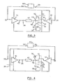
Un autre dispositif connu, représenté schématiquement en figure 1, consiste à connecter deux amplificateurs classe B1 et 2, alimentés par la même source d'alimentation 3, la charge 4 étant connectée entre les deux bornes de sortie 5 et 6 des amplificateurs. La borne d'entrée 7 de l'amplificateur 1 reçoit le signal à amplifier, alors que la borne d'entrée 8 de l'amplificateur 2 reçoit l'opposé de ce signal. Cette disposition a un rendement identique à celui d'un amplificateur classe B unique, mais permet en outre d'obtenir sur la charge une tension comprise entre + V et - V, V étant la tension de la source d'alimentation unique 3.Another known device, shown diagrammatically in FIG. 1, consists in connecting two class B1 and 2 amplifiers, supplied by the
Un autre dispositif connu, du même type que celui décrit dans le document DE-A-2 304 162, est représenté schématiquement à la figure 2. Ce dispositif, connu sous le nom d'amplificateur classe G, comprend deux amplificateurs en classe B imbriqués et alimentés par des tensions d'alimentation différentes. Les transistors 20 et 21 forment un premier amplificateur en classe B, alimenté par l'intermédiaire des diodes 28 et 29 par la source d'alimentation à point milieu formée par les sources de tension 30 et 31 connectées en série. La charge 34, étant connectée entre la borne de sortie 35 de cet amplificateur et le point milieu 36 des sources, est soumise à une tension de sortie qui peut varier entre + V et - V, V étant la tension aux bornes des sources de tension 30 ou 31. En supposant que les transistors 20 et/ou 21 sont saturés, des transistors 22 et 23, connectés en série avec ceux-ci de la façon représentée sur la figure, forment un deuxième amplificateur en classe B, alimenté par la source à point milieu formée par les sources de tension en série 30, 31, 32 et 33. On utilise généralement des sources 32 et 33 avant la même tension V'. Lorsque ce deuxième amplificateur est en fonctionnement, la tension aux bornes de la charge 34, toujours connectée entre la borne de sortie 35 de l'amplificateur et le point milieu 36 des sources, est soumise à une tension pouvant varier de - (V + V') à + (V + V'). Les diodes 24, 25, 26 et 27 connectées aux bases des transistors 20, 21, 22 et 23 forment un ensemble de communication permettant de commander soit le premier amplificateur, soit le second amplificateur suivant le niveau de la tension d'entrée appliquée à la borne d'entrée 37. Cette disposition permet, lorsque le signal d'entrée sur la borne 37 est faible, de commander uniquement le premier amplificateur en classe B constitué par les transistors 20 et 21. Cet amplificateur, alimenté par les sources de tension 30 et 31, fonctionne dans de meilleures conditions que s'il était alimenté par la source de tension maximale formée par 30, 31, 32 et 33. Ainsi, son rendement est supérieur à celui qui serait obtenu par un amplificateur en classe B seul alimenté par la tension maximale. De même, lorsque la tension d'entrée sur la borne 37 est grande, la tension de sortie aux bornes de la charge 34 devant dépasser la valeur V des sources 30 et 31, le deuxième amplificateur formé par les transistors 22 et 23 est alors commandé. Il permet d'amplifier les parties de signal correspondant à des tensions de sortie supérieures à V, et pouvant aller jusqu'à V + V'. Le second amplificateur travaille alors également dans de bonnes conditions, puisque sa tension de sortie est voisine de la tension maximale admissible. L'amplificateur en classe G ainsi décrit a un rendement supérieur au rendement d'un amplificateur en classe B, ou de deux amplificateurs en pont tels que décrits à la figure 1. Néanmoins, il ne permet pas de fournir sur la charge une tension crête supérieure à la moitié de la tension maximale d'alimentation formée par la somme des tensions des sources 30, 31, 32 et 33, et en outre il nécessite la présence de plusieurs sources d'alimentation de puissance.Another known device, of the same type as that described in document DE-A-2,304,162, is shown diagrammatically in FIG. 2. This device, known under the name of class G amplifier, comprises two nested class B amplifiers and supplied by different supply voltages. The
La présente invention vise notamment à réaliser des amplificateurs de puissance pour audio- fréquence ayant un rendement aussi bon que celui des amplificateurs classe G en réduisant le nombre des sources d'alimentation de puissance nécessaires.The present invention aims in particular to produce power amplifiers for audio-frequency having a performance as good as that of class G amplifiers by reducing the number of power supply sources required.
De même, la présente invention vise à réaliser des amplificateurs présentant les avantages du dispositif de l'art antérieur décrit à la figure 1, c'est-à-dire d'une part ne nécessitant qu'une seule source d'alimentation de puissance de tension V, fournissant sur la charge une tension crête égale à + V, et présentant l'avantage d'un bon rendement tel que celui de l'amplificateur en classe G de la figure 2.Likewise, the present invention aims to produce amplifiers having the advantages of the device of the prior art described in FIG. 1, that is to say on the one hand requiring only a single power supply source. of voltage V, providing on the load a peak voltage equal to + V, and having the advantage of a good efficiency such as that of the amplifier in class G of FIG. 2.
Pour atteindre ces objets ainsi que d'autres, la présente invention prévoit un dispositif amplificateur pour audio-fréquences, comprenant un premier et un second amplificateurs, le premier amplificateur étant alimenté par une source d'alimentation de tension V1 dont les deux bornes de sortie sont à des potentiels symétriques par rapport à une borne de potentiel zéro, ledit dispositif amplificateur débitant sur une charge comportant des première et seconde bornes, la première borne étant reliée à la borne de sortie du premier amplificateur, le second amplificateur étant alimenté par une tension d'alimentation V2 dont les bornes sont à des potentiels symétriques par rapport à la borne de potentiel zéro, ce dispositif comprenant aussi des moyens de commutation à deux états et des moyens de commande pour forcer les moyens de commutation dans l'un ou l'autre de leurs états suivant le niveau du signal à amplifier par le dispositif amplificateur, les moyens de commutation connectant dans le premier état la deuxième borne de la charge à la borne de sortie du second amplificateur et dans le deuxième état la deuxième borne de la charge à la borne de potentiel zéro et comprenant en outre des moyens de transmission pour appliquer au second amplificateur un signal d'entrée fonction du signal à amplifier dès que ce signal a atteint et dépassé un niveau amenant le premier amplificateur à la saturation.To achieve these and other objects, the present invention provides an amplifier device for audio frequencies, comprising first and second amplifiers, the first amplifier being supplied by a voltage supply source V1, the two output terminals of which are at symmetrical potentials with respect to a zero potential terminal, said amplifier device debiting on a load comprising first and second terminals, the first terminal being connected to the output terminal of the first amplifier, the second amplifier being supplied by a voltage supply V2 whose terminals are at symmetrical potentials with respect to the zero potential terminal, this device also comprising two-state switching means and control means for forcing the switching means into one or the other of their states according to the level of the signal to be amplified by the amplifying device, the switching means connecting in the p reset the second terminal of the load to the output terminal of the second amplifier and in the second state the second terminal of the load to the zero potential terminal and further comprising transmission means for applying to the second amplifier a signal input function of the signal to be amplified as soon as this signal has reached and exceeded a level bringing the first amplifier to saturation.
Selon un autre aspect de la présente invention, le second amplificateur est également alimenté par la source d'alimentation V1, la source d'alimentation V2 étant supprimée. L'ensemble ne comporte ainsi qu'une seule source d'alimentation de puissance.According to another aspect of the present invention, the second amplifier is also supplied by the power source V1, the power source V2 being eliminated. The assembly thus comprises only one power supply source.
Selon un autre aspect de la présente invention, la borne de potentiel zéro est connectée à une borne d'un condensateur de forte valeur, l'autre borne de ce condensateur étant connectée à l'une des bornes de la source d'alimentation.According to another aspect of the present invention, the zero potential terminal is connected to a terminal of a high value capacitor, the other terminal of this capacitor being connected to one of the terminals of the power source.
Selon un autre aspect de la présente invention, le dispositif de commande est tel qu'il provoque la connexion de la charge à la borne de potentiel zéro lorsque le signal d'entrée est inférieur au seuil prédéterminé correspondant à la saturation du premier amplificateur, et la connexion de la charge à la borne de sortie du second amplificateur lorsque le signal d'entrée est supérieur audit seuil.According to another aspect of the present invention, the control device is such that it causes the load to be connected to the zero potential terminal when the input signal is less than the predetermined threshold corresponding to the saturation of the first amplifier, and connecting the load to the output terminal of the second amplifier when the input signal is greater than said threshold.
Selon un autre aspect de la présente invention, les moyens de commutation comprennent au moins un transistor à effet de champ, connecté entre la charge et la borne de potentiel zéro.According to another aspect of the present invention, the switching means comprise at least one field effect transistor, connected between the load and the zero potential terminal.
Selon un autre aspect de la présente invention, les moyens pour appliquer au second amplificateur un signal d'entrée comprennent un inverseur dont l'entrée est connectée à la borne d'entrée du dispositif amplificateur, et dont la borne de sortie est connectée à l'une des deux entrées d'un dispositif additionneur produisant sur sa borne de sortie connectée à l'entrée du deuxième amplificateur un signal égal à la somme des signaux appliqués sur ces deux entrées. La seconde entrée du dispositif additionneur est connectée à la sortie du premier amplificateur par l'intermédiaire d'un pont diviseur de résistances de rapport 1/G, G étant le gain de ce premier amplificateur.According to another aspect of the present invention, the means for applying an input signal to the second amplifier include an inverter whose input is connected to the input terminal of the amplifier device, and whose output terminal is connected to the one of the two inputs of an adder device producing on its output terminal connected to the input of the second amplifier a signal equal to the sum of the signals applied to these two inputs. The second input of the adder device is connected to the output of the first amplifier by means of a resistor divider bridge of
Ces objets, caractéristiques et avantages ainsi que d'autres de la présente invention seront exposés plus en détail dans la description suivante de modes de réalisation particuliers, faite en relation avec les figures jointes parmi lesquelles :
- la figure 1 est destinée à illustrer un dispositif de l'art antérieur ;
- la figure 2 représente un autre dispositif de l'art antérieur ;
- la figure 3 représente schématiquement un mode de réalisation particulier du dispositif selon l'invention ;
- la figure 4 représente un autre mode de réalisation d'un dispositif selon l'invention ; et
- la figure 5 représente de façon plus détaillée le dispositif selon le mode de réalisation de la figure 4.
- Figure 1 is intended to illustrate a device of the prior art;
- FIG. 2 represents another device of the prior art;
- FIG. 3 schematically represents a particular embodiment of the device according to the invention;
- FIG. 4 represents another embodiment of a device according to the invention; and
- FIG. 5 shows in more detail the device according to the embodiment of FIG. 4.
Comme cela est représenté schématiquement à la figure 3, le dispositif amplificateur selon la présente invention comprend deux amplificateurs 41 et 42 alimentés par une source d'alimentation formée par les sources de tension 43 et 44 de tension égale V connectées en série. Chacun des deux amplificateurs 41 et 42 est capable de fournir sur sa borne de sortie, respectivement 45 et 46, un potentiel pouvant varier entre le potentiel le plus négatif et le potentiel le plus positif de la source d'alimentation 43-44, et admettant un courant de sortie dans les deux sens. La borne de sortie 45 de l'amplificateur 41 est connectée à une borne 56 de la charge 47. La seconde borne 48 de la charge est connectée à une borne de sortie 49 d'un sous-ensemble de commutation 50. Ce dispositif de commutation comporte deux autres bornes de sortie, la borne 51 qui est connectée à la borne de sortie 46 de l'amplificateur 42, et la borne 52 qui est connectée à la borne 53, point commun des sources d'alimentation 43 et 44. La borne 53 est appelée borne de potentiel zéro. Le sous-ensemble de commutation 50 est commandé par l'intermédiaire d'une liaison représentée en pointillés 54 par un sous-ensemble de commande 55. Le sous-ensemble de commutation 50 remplit la fonction d'un interrupteur inverseur, pouvant se situer notamment dans les deux états suivants : dans l'état 1 la borne 49 est connectée électriquement à la borne 51, la borne 52 étant Isolée des bornes 49 et 51 ; dans l'état Il la borne 49 est connectée à la borne 52, la borne 51 étant isolée des bornes 49 et 52. La borne d'entrée 57 de l'amplificateur 41 reçoit le signal à amplifier. La borne d'entrée 58 de l'amplificateur 42 est connectée à la borne de sortie 59 d'un sous-ensemble de transmission 60 dont une borne d'entrée 61 est connectée à la borne d'entrée 57 de l'amplificateur 41.As shown schematically in Figure 3, the amplifier device according to the present invention comprises two
Le fonctionnement du dispositif est le suivant :
- Lorsque le sous-
ensemble de commutation 50 est enposition 1, lacharge 47 est soumise à la différence des tensions de sortie des amplificateurs 41et 42. Cette tension aux bornes de la charge peut donc prendre toute valeur comprise entre + 2 V et - 2 V. Lorsque l'un des amplificateurs est saturé, par exemple lorsque l'amplificateur 41 a sa borne de sortie 45 au potentiel maximum, la tension aux bornes de lacharge 47 ne dépend plus que de la tension de sortie de l'amplificateur 42. Cette tension est alors fonction du signal d'entrée présent à la borne 57 qui est transmis par l'intermédiaire de l'élément detransmission 60 à la borne d'entrée de l'amplificateur 42.
- When the switching
subassembly 50 is inposition 1, theload 47 is subjected to the difference of the output voltages of theamplifiers amplifier 41 has itsoutput terminal 45 at maximum potential, the voltage at the terminals of theload 47 only depends on the output voltage of theamplifier 42. This voltage is then a function of the input signal present atterminal 57 which is transmitted via thetransmission element 60 to the input terminal ofamplifier 42.
Lorsque le sous-ensemble de commutation est en position II, la charge est connectée entre la sortie de l'amplificateur 41 et la borne 53 de potentiel zéro. Il faut remarquer que la source d'alimentation formée par les deux sources de tension 43 et 44 en série a ses deux bornes de sortie à des potentiels symétriques par rapport à la borne 53 de potentiel zéro. Dans cette position Il du dispositif de commutation 50, la tension aux bornes de la charge 47 ne dépend que de la tension de sortie de l'amplificateur 41. Cette tension peut donc prendre toute valeur comprise entre + V et - V. Le dispositif amplificateur se comporte alors comme un amplificateur en classe B.When the switching sub-assembly is in position II, the load is connected between the output of the
Il est prévu, selon une caractéristique de la présente invention, d'utiliser ce dispositif de la manière suivante : lorsque le signal d'entrée sur la borne 57 a une valeur faible, c'est-à-dire de module inférieur à un certain seuil correspondant à la saturation de l'amplificateur 41, le sous-ensemble de commande 55 force le dispositif de commutation 50 dans l'état II. L'amplificateur 41 fournit alors seul le courant nécessaire à la charge 47, l'amplificateur 42 n'étant parcouru par aucun courant de charge et dissipant donc une puissance négligeable. Par contre, lorsque le signal présent à la borne d'entrée 57 est supérieur au seuil de saturation de l'amplificateur 41, le sous-ensemble de commande 55 force le dispositif de commutation 50 dans l'état I, mettant ainsi en fonctionnement le deuxième amplificateur 42. Pendant tout le temps où le signal à l'entrée reste supérieur au seuil de saturation, l'amplificateur 41 reste saturé, sa borne de sortie 45 étant à un potentiel fixe voisin du potentiel de l'une des deux bornes extrêmes de la source d'alimentation. Cet amplificateur 41 est parcouru par le courant traversant la charge, mais étant donné son état de saturation, la puissance qu'il dissipe est très faible. L'ensemble de transmission 60 et l'amplificateur 42, sous l'action du signal d'entrée à la borne 57, fournissent sur la charge 47 le complément de tension correspondant à la partie du signal d'entrée qui dépasse le seuil de saturation de l'amplificateur 41. Pour cela, le sous-ensemble de transmission 60 fournit à sa borne de sortie 59 un signal égal à la différence entre d'une part le signal d'entrée présent à la borne 57 et d'autre part la tension d'entrée qui suffit à provoquer la saturation de l'amplificateur 41. Cette différence, appliquée avec un signe convenable à l'entrée de l'amplificateur 42, permet d'obtenir sur la borne de sortie 46 dudit amplificateur la tension complémentaire à la tension déjà fournie par la borne de sortie 45 de l'amplificateur 41 en état de saturation. Lorsqu'un signal variable est appliqué à l'entrée 57, le sous-ensemble 55 de commande réagit de façon à forcer la commutation du dispositif 50 chaque fois que la valeur absolue du signal d'entrée dépasse ou devient inférieure à la tension de seuil de saturation de l'amplificateur 41.It is planned, according to a characteristic of the present invention, to use this device in the following manner: when the input signal on
Le dispositif ainsi utilisé permet d'obtenir les avantages suivants : d'une part, la tension maximale possible sur la charge 47 est égale à 2 V ; d'autre part, dans les deux modes d'utilisation, c'est-à-dire lorsque l'amplificateur 41 fonctionne seul ou lorsque les deux amplificateurs 41 et 42 fonctionnent ensemble, la puissance dissipée au niveau de ces amplificateurs est égale à la puissance que dissiperait un amplificateur en classe B dont la tension d'alimentation est égale à 2 V lorsque le signal d'entrée est faible et est égale à 4 V lorsque le signal d'entrée est grand. Cela conduit à utiliser ces amplificateurs en classe B dans des conditions qui leur sont plus favorables au point de vue rendement, c'est-à-dire dans des conditions où la tension de sortie est la plus proche de la tension maximale admissible. De même, on peut considérer que ce dispositif permet de réaliser un amplificateur audiofréquence ayant les mêmes caractéristiques de rendement qu'un amplificateur en classe G à quatre sources d'alimentation tel que décrit à la figure 2.The device thus used makes it possible to obtain the following advantages: on the one hand, the maximum possible voltage on the
La figure 4 reprend les principaux éléments du dispositif représentés en figure 3, et représente un mode de réalisation particulier d'un dispositif amplificateur selon l'invention. Comme cela est représenté sur la figure, selon ce mode de réalisation, le dispositif ne comprend qu'une seule source d'alimentation 70 alimentant les deux amplificateurs 41 et 42. Dans ce cas, la borne 53 de potentiel zéro est connectée à l'une des bornes de sortie de la source d'alimentation 70 par l'intermédiaire d'un condensateur 71 de forte valeur. On a représenté sur la figure une connexion de ce condensateur à la borne négative de la source d'alimentation. Ce mode de réalisation est satisfaisant pour les applications où la tension aux bornes de la charge doit avoir une valeur moyenne nulle. En effet, pendant les alternances positives, le condensateur se charge dans un certain sens, et pendant les alternances négatives, le condensateur se décharge de la même valeur dans l'autre sens la valeur de sa tension n'ayant pas le temps de varier de façon sensible. On a ainsi réalisé un dispositif amplificateur selon l'invention ne comportant qu'une seule source d'alimentation au lieu de deux sources pour le mode de réalisation précédent, et de quatre sources pour les réalisations connues telles que représentées à la figure 2.Figure 4 shows the main elements of the device shown in Figure 3, and shows a particular embodiment of an amplifier device according to the invention. As shown in the figure, according to this embodiment, the device comprises only a
La figure 5 reprend les principaux éléments représentés en figure 4 avec la même disposition de connexion électrique et fournit une représentation plus détaillée des sous-ensembles de commande 55 et de transmission 60. L'amplificateur 41 est connecté par sa sortie 45 à la charge 47, une autre borne de la charge étant connectée à la borne 49 du dispositif de commutation 50, la sortie de l'amplificateur 42 étant connectée à une autre borne 51 de ce même dispositif de commutation 50. La borne de potentiel zéro 53 est connectée à une autre borne de sortie 52 du dispositif 50. Selon ce mode de réalisation, ce dispositif 50 comprend deux transistors à effet de champ 72 et 73 de type MOS connectés de la façon suivante : le transistor 72 a son drain connecté à la borne de sortie 52, sa source connectée à la borne de sortie 49 du dispositif de commutation 50, et sa grille connectée à une borne de sortie 74 du sous-ensemble de commande 55. Le transistor 73 a sa source connectée à la borne de sortie 51, son drain connecté à la borne de sortie 49 du dispositif de commutation, et sa grille connectée à une borne de sortie 75 du sous-ensemble de commande 55. Ces deux connexions de grille aboutissant aux bornes 74 et 75 du dispositif de commande sont un mode de réalisation de la liaison, figurée par les pointillés 54 de la figure 3, entre le dispositif de commutation 50 et le sous-ensemble de commande 55.FIG. 5 shows the main elements represented in FIG. 4 with the same electrical connection arrangement and provides a more detailed representation of the
Le sous-ensemble de commande 55, selon ce mode de réalisation, comprend une borne d'entrée 76 connectée à la borne d'entrée 57 du dispositif d'amplification. Un comparateur 77 a une première borne d'entrée connectée à la borne d'entrée 76, une seconde borne d'entrée connectée à la borne positive d'une source de tension 78 dont la borne négative est connectée à la masse, et une borne de sortie connectée à une première borne d'entrée d'une porte logique ou 81. Un second comparateur 79 a une borne d'entrée connectée à la borne d'entrée 76, une autre borne d'entrée connectée à la borne négative d'une source de tension 80 dont la borne positive est connectée à un point de potentiel zéro, et une borne de sortie connectée à l'autre borne d'entrée de la porte logique 81. La borne de sortie de la porte OU 81 est connectée à la borne d'entrée d'un dispositif amplificateur 82. Ce dispositif 82 a deux bornes de sortie connectées respectivement à la borne de sortie 74 et à la borne 75 du sous-ensemble de commande 55. Le dispositif 82 est réalisé par tout moyen bien connu dans la technique pour commander deux transistors à effet de champ de type MOS à partir d'une tension d'entrée fournie par la porte logique 81. Les sources de tension 78 et 80 sont de valeur égale, cette valeur correspondant au seuil de saturation de l'amplificateur 41, c'est-à-dire à la tension qui, appliquée à la borne 57, provoque la saturation de cet amplificateur.The
Ces sources de tension 78 et 80 sont des sources de référence de faible puissance réalisées dans la pratique par tout moyen bien connu dans la technique, par exemple par dérivation aux bornes de la source d'alimentation principale 70 au moyen de ponts de résistances. Pour simplifier la description et les figures, elles sont représentées sous forme de sources de tension indépendantes.These
Le sous-ensemble de transmission 60, comportant une borne d'entrée 61 connectée à la borne d'entrée 57 du dispositif, et une borne de sortie 59 connectée à la borne d'entrée de l'amplificateur 42, est réalisé selon ce mode de réalisation de la façon suivante. Un inverseur 83 a sa borne d'entrée connectée à la borne 61, et sa borne de sortie connectée à une première entrée d'un additionneur 84, dont la sortie est connectée à la borne 59, et dont la deuxième entrée est connectée à la masse par l'intermédiaire d'une résistance 85. Une résistance 86 est connectée entre la seconde entrée de l'additionneur 84 et une borne d'entrée 87 du sous-ensemble de transmission 60. La borne d'entrée 87 est connectée à la borne de sortie 45 de l'amplificateur 41. Le pont de résistances 85-86 est un diviseur de tension. La valeur des résistances 85 et 86 est choisie de façon à ce que la tension de sortie de l'amplificateur 41 soit divisée, pour être appliquée à l'entrée de l'additionneur 84, par un facteur G, G étant le gain de l'amplificateur 41.The
Le fonctionnement du dispositif est le suivant :
- Supposons dans un premier temps que le signal appliqué sur la borne
d'entrée 57 du dispositif amplificateur est faible, c'est-à-dire inférieur au seuil provoquant .la saturation de l'amplificateur 41. Le signal, appliqué sur les deux entrées des comparateurs 77et 79, est tel que la sortie de ces deux comparateurs est au niveau logique zéro. La sortie de laporte OU 81 est donc également au niveau logique zéro. Le dispositif amplificateur 82 fournit alors sur ses bornes de sortie 74 et 75 des tensions de commande telles que le transistor à effet dechamp 72 soit conducteur et le transistor à effet dechamp 73 soit bloqué. Ainsi, lacharge 47 se trouve connectée entre la borne 53 de potentiel zéro et la borne de sortie de l'amplificateur 41. Cet amplificateur fournit le courant nécessaire à la charge et amplifie la tension du signal d'entrée présent à la borne 57.L'amplificateur 42, dont la sortie est en série avec le transistor à effet dechamp 73 bloqué, ne débite aucun courant.
- Let us first assume that the signal applied to the
input terminal 57 of the amplifier device is weak, that is to say below the threshold causing the saturation of theamplifier 41. The signal, applied to the twoinputs comparators OR gate 81 is therefore also at logic level zero. Theamplifier device 82 then supplies control voltages on itsoutput terminals field effect transistor 72 is conductive and thefield effect transistor 73 is blocked. Thus, theload 47 is connected between the terminal 53 of zero potential and the output terminal of theamplifier 41. This amplifier supplies the current necessary for the load and amplifies the voltage of the input signal present at the terminal 57. Theamplifier 42, the output of which is in series with the blockedfield effect transistor 73, does not deliver any current.
Lorsque le signai, partant d'une valeur positive faible, augmente, il atteint le seuil de saturation de l'amplificateur 41. A cet instant, le comparateur 77 change d'état, sa sortie passant au niveau logique 1, ce qui provoque l'apparition d'un niveau logique 1 à la sortie de la porte 81. Le dispositif 82 produit alors sur ses bornes de sortie 74 et 75 des tensions telles que le transistor MOS 72 se bloque, et le transistor 73 est conducteur. Dans ces conditions, la charge 47 se trouve connectée entre la borne de sortie de l'amplificateur 41 en état de saturation, et la borne de sortie de l'amplificateur 42. Le diviseur de tension formé par les résistances 85 et-86 fournit alors sur la borne d'entrée de l'additionneur 84 une tension égale à la tension de seuil de saturation de l'amplificateur 41 avec un signe convenable. Cette tension, additionnée à l'opposé du signal d'entrée de la borne 57, produit par l'inverseur 83, fournit à la borne 59 une tension dont le module est égal à la partie du signal d'entrée qui n'est pas amplifiée par l'amplificateur 41 en état de saturation, et de signe opposé. L'amplificateur 42 fournit ainsi sur sa borne de sortie une tension complémentaire de la tension fournie par l'amplificateur 41, ceci à condition qu'il ait le même gain G.When the signal, starting from a low positive value, increases, it reaches the saturation threshold of the
Dans le cas où le signal d'entrée devient négatif et supérieur en valeur absolue au seuil de saturation de l'amplificateur 41, la sortie du comparateur 77 reste à l'état logique 0, mais la sortie du comparateur 79 passe à un niveau logique 1, ce qui fait apparaître un niveau logique 1 à la sortie de la porte 81, provoquant, de même que précédemment, le blocage du transistor 72 et la conduction du transistor 73. Le fonctionnement est alors le même que dans le cas d'un signal positif supérieur au seuil de saturation.In the case where the input signal becomes negative and greater in absolute value than the saturation threshold of the
Ce mode de réalisation, décrit en relation avec la figure 5, est susceptible de variantes. Par exemple, si l'amplificateur 42 présente une forte impédance de sortie lorsqu'il n'est pas commandé, il est alors possible de supprimer le transistor à effet de champ MOS 73. Pour cela, il suffit de prévoir en série avec l'entrée de cet amplificateur 42 un dispositif interrupteur pour déconnecter cette entrée lorsque l'amplificateur 42 ne doit pas être utilisé, c'est-à-dire lorsque le signal d'entrée à la borne 57 est faible. Notamment, on pourra prévoir de placer un transistor à effet de champ tel que 73 non plus à la sortie de l'amplificateur 42 mais en série avec son entrée. Le transistor 73 pourra alors être un transistor à effet de champ de faible puissance.This embodiment, described in relation to FIG. 5, is susceptible of variants. For example, if the
Une autre variante de ce mode de réalisation consiste à connecter la borne d'entrée 76 du sous-ensemble de commande 55 non plus à la borne d'entrée 57 mais à la borne de sortie 45 de l'amplificateur 41. Dans ces conditions, pour obtenir le même fonctionnement, il suffit de prévoir des sources de tension 78 et 80 dont la valeur est voisine de la tension que présente la sortie 45 de l'amplificateur 41 lorsqu'il est saturé.Another variant of this embodiment consists in connecting the
Dans ce qui précède, on a supposé que les deux amplificateurs 41 et 42 ont le même gain G et sont alimentés par une tension d'alimentation identique. Dans ces conditions, si S est la valeur maximale du signal d'entrée présent à la borne 57, la commutation de l'amplificateur 42 se produit au moment où le signal d'entrée atteint la moitié de sa valeur maximale, c'est-à-dire S/2. Il est possible de prévoir un dispositif pour lequel la commutation se produit pour une valeur différente de ce signal d'entrée. Pour cela, on peut prévoir un dispositif comportant deux sources d'alimentation, une première source telle que 70 alimentant l'amplificateur 41, de tension égale à 2 V, et une seconde source d'alimentation de tension 2 V' alimentant l'amplificateur 42. La première source 70 a, comme dans les modes de réalisation précédents, des potentiels sur ses deux bornes de sortie qui sont symétriques par rapport au potentiel de la borne 53 de potentiel zéro. De même, il faut que la seconde source de potentiel 2 V' ait ses deux bornes de sortie à des potentiels symétriques par rapport à la même borne de potentiel zéro. Ceci peut être réalisé par tout moyen bien connu dans la technique. La tension sur la charge 47 sera alors comprise entre + (V + V') et - (V + V'). Dans le cas où, par exemple, V' est égal au double de V, la commutation de l'amplificateur 42 se produira lorsque le signal d'entrée sur la borne 57 est égal au tiers de sa valeur maximale admissible. Une telle disposition peut avoir un intérêt si le signal d'entrée à amplifier est presque toujours inférieur au tiers de sa valeur maximale.In the foregoing, it has been assumed that the two
Claims (8)
Applications Claiming Priority (2)
| Application Number | Priority Date | Filing Date | Title |
|---|---|---|---|
| FR7916558 | 1979-06-27 | ||
| FR7916558A FR2460070A1 (en) | 1979-06-27 | 1979-06-27 | AMPLIFIER DEVICE FOR AUDIO-FREQUENCIES |
Publications (2)
| Publication Number | Publication Date |
|---|---|
| EP0022015A1 EP0022015A1 (en) | 1981-01-07 |
| EP0022015B1 true EP0022015B1 (en) | 1983-08-03 |
Family
ID=9227173
Family Applications (1)
| Application Number | Title | Priority Date | Filing Date |
|---|---|---|---|
| EP80400939A Expired EP0022015B1 (en) | 1979-06-27 | 1980-06-24 | Amplifier arrangement and method of amplification for audio frequencies |
Country Status (5)
| Country | Link |
|---|---|
| US (1) | US4330756A (en) |
| EP (1) | EP0022015B1 (en) |
| JP (1) | JPS566506A (en) |
| DE (1) | DE3064484D1 (en) |
| FR (1) | FR2460070A1 (en) |
Cited By (1)
| Publication number | Priority date | Publication date | Assignee | Title |
|---|---|---|---|---|
| SG80090A1 (en) * | 1999-01-29 | 2001-04-17 | Cit Alcatel | Power amplifier arrangement |
Families Citing this family (11)
| Publication number | Priority date | Publication date | Assignee | Title |
|---|---|---|---|---|
| JPS5717204A (en) * | 1980-07-04 | 1982-01-28 | Fujitsu Ltd | Transient sound prevention type power amplifying circuit |
| IT1237511B (en) * | 1989-10-31 | 1993-06-08 | Sgs Thomson Microelectronics | HIGH EFFICIENCY AUDIO AMPLIFICATION CIRCUIT, WITH SWITCHING OF THE OPERATING STATUS ACCORDING TO THE INPUT SIGNAL |
| IT1243920B (en) * | 1990-11-20 | 1994-06-28 | Sgs Thomson Microelectronics | HIGH EFFICIENCY AUDIO POWER AMPLIFIER COMPOSED OF TWO AMPLIFIERS WITH A SINGLE POWER SUPPLY. |
| NL9100115A (en) * | 1991-01-24 | 1992-08-17 | Philips Nv | SWITCHING BRIDGE AMPLIFIER. |
| GB2287147A (en) * | 1994-02-26 | 1995-09-06 | Motorola Inc | Bridge circuit for driving a loudspeaker either from one end to earth or from both ends |
| EP0855101B1 (en) * | 1996-08-09 | 2005-09-07 | Koninklijke Philips Electronics N.V. | An amplifier and a method for detecting the presence of a load |
| EP1487100A1 (en) * | 2003-06-09 | 2004-12-15 | STMicroelectronics S.r.l. | Multi-channel power amplifier with channels independently self-configuring bridge or single-ended output, particulary for audio applications |
| EP1496611A1 (en) * | 2003-07-09 | 2005-01-12 | STMicroelectronics S.r.l. | Multi-channel power amplifier self-configuring to a bridge or single-ended output, particularly for audio applications |
| US7362169B2 (en) * | 2005-04-04 | 2008-04-22 | Gang Liu | Power efficient amplifier |
| US7821338B2 (en) * | 2008-04-18 | 2010-10-26 | Fairchild Semiconductor Corporation | Amplifier current drive reversal |
| CN107846199B (en) * | 2016-09-21 | 2022-09-30 | 北京普源精电科技有限公司 | Dual-channel power amplifier |
Family Cites Families (3)
| Publication number | Priority date | Publication date | Assignee | Title |
|---|---|---|---|---|
| DE1960841A1 (en) * | 1969-12-04 | 1971-06-16 | Bodenseewerk Geraetetech | Class B push-pull power amplifier for servo circuits on gyro-stabilized platforms |
| DE2304162C3 (en) * | 1973-01-29 | 1976-01-08 | Robert 5300 Bonn Sczech | Electronic amplifier with high efficiency or low electrical power loss |
| DE2705604C3 (en) * | 1976-02-12 | 1979-12-20 | Hitachi, Ltd., Tokio | NF power amplifier |
-
1979
- 1979-06-27 FR FR7916558A patent/FR2460070A1/en active Granted
-
1980
- 1980-06-24 EP EP80400939A patent/EP0022015B1/en not_active Expired
- 1980-06-24 DE DE8080400939T patent/DE3064484D1/en not_active Expired
- 1980-06-25 US US06/162,740 patent/US4330756A/en not_active Expired - Lifetime
- 1980-06-27 JP JP8767780A patent/JPS566506A/en active Pending
Cited By (1)
| Publication number | Priority date | Publication date | Assignee | Title |
|---|---|---|---|---|
| SG80090A1 (en) * | 1999-01-29 | 2001-04-17 | Cit Alcatel | Power amplifier arrangement |
Also Published As
| Publication number | Publication date |
|---|---|
| US4330756A (en) | 1982-05-18 |
| EP0022015A1 (en) | 1981-01-07 |
| JPS566506A (en) | 1981-01-23 |
| DE3064484D1 (en) | 1983-09-08 |
| FR2460070A1 (en) | 1981-01-16 |
| FR2460070B1 (en) | 1981-08-14 |
Similar Documents
| Publication | Publication Date | Title |
|---|---|---|
| EP0022015B1 (en) | Amplifier arrangement and method of amplification for audio frequencies | |
| WO2002054167A1 (en) | Voltage regulator with enhanced stability | |
| FR2479606A1 (en) | POWER SUPPLY PREAMPLIFIER FOR ONE OR MORE DIFFERENTIAL AMPLIFIERS | |
| EP1085659B1 (en) | Current type digital to analogue converters | |
| FR2589649A1 (en) | DEVICE FOR INCREASING THE OUTPUT POWER OF A LOW VOLTAGE POWERED RADIO APPARATUS, FOR EXAMPLE OF THE AUTORADIO TYPE | |
| FR2694851A1 (en) | Draw circuit to a determined state of an integrated circuit input. | |
| FR2547126A1 (en) | CURRENT VOLTAGE CONVERTING CIRCUIT | |
| EP0737003B1 (en) | CCD register readout amplifier | |
| EP0271938B1 (en) | Automatic gain-controlled amplifier circuit | |
| EP0613241B1 (en) | Output common-mode voltage control device of a balanced amplifier | |
| EP0318379A1 (en) | Ultra-high frequency amplifier with a very wide pass band | |
| FR2582169A1 (en) | AMPLIFIER APPARATUS | |
| FR2611283A1 (en) | DEVICE COMPRISING AN ELECTRONIC CIRCUIT FOR PROCESSING AN ANALOG SIGNAL | |
| EP0060164A1 (en) | Sliding class A broadband linear amplifier with low power consumption, and circuit comprising at least one such amplifier | |
| FR2527399A1 (en) | CIRCUIT WITH IMPEDANCE OF ENTRANCE, HIGH | |
| WO2002052364A1 (en) | Voltage regulator with static gain in reduced open loop | |
| EP1870716A1 (en) | Device for detecting broadband microwave frequencies | |
| FR2477340A1 (en) | AMPLIFIER CIRCUIT WHOSE TOTAL AMPLIFICATION CAN BE CONTROLLED BY CONTROL VOLTAGE | |
| FR2589648A1 (en) | FIELD EFFECT TRANSISTOR AMPLIFIER CIRCUIT | |
| EP0050583B1 (en) | Alternating voltage to direct current converter and oscillator circuit comprising said converter | |
| FR2872648A1 (en) | FAST TRANSCONDUCTANCE AMPLIFIER | |
| FR2638309A1 (en) | PLATE FOR PRETREATMENT OF EXIT CURRENTS OF DETECTION DIODES SUBJECTED TO THERMAL RADIATION | |
| EP1296446A1 (en) | Balanced Mixer using bipolar Transistors | |
| EP1215891A1 (en) | Charge reading circuit and method with adaptative preamplification | |
| FR2882204A1 (en) | Broadband microwave monolithic integrated circuit amplifier circuit for optical telecommunication application, has short-circuit series resistor of gate of each polarization transistor of polarization cell with its source integrated to cell |
Legal Events
| Date | Code | Title | Description |
|---|---|---|---|
| PUAI | Public reference made under article 153(3) epc to a published international application that has entered the european phase |
Free format text: ORIGINAL CODE: 0009012 |
|
| AK | Designated contracting states |
Designated state(s): DE GB IT |
|
| 17P | Request for examination filed |
Effective date: 19810123 |
|
| ITF | It: translation for a ep patent filed |
Owner name: JACOBACCI & PERANI S.P.A. |
|
| RBV | Designated contracting states (corrected) |
Designated state(s): DE GB IT |
|
| GRAA | (expected) grant |
Free format text: ORIGINAL CODE: 0009210 |
|
| STAA | Information on the status of an ep patent application or granted ep patent |
Free format text: STATUS: THE PATENT HAS BEEN GRANTED |
|
| AK | Designated contracting states |
Designated state(s): DE GB IT |
|
| REF | Corresponds to: |
Ref document number: 3064484 Country of ref document: DE Date of ref document: 19830908 |
|
| PLBE | No opposition filed within time limit |
Free format text: ORIGINAL CODE: 0009261 |
|
| 26N | No opposition filed | ||
| ITTA | It: last paid annual fee | ||
| PGFP | Annual fee paid to national office [announced via postgrant information from national office to epo] |
Ref country code: GB Payment date: 19990623 Year of fee payment: 20 |
|
| PGFP | Annual fee paid to national office [announced via postgrant information from national office to epo] |
Ref country code: DE Payment date: 19990626 Year of fee payment: 20 |
|
| PG25 | Lapsed in a contracting state [announced via postgrant information from national office to epo] |
Ref country code: GB Free format text: LAPSE BECAUSE OF EXPIRATION OF PROTECTION Effective date: 20000623 |
|
| REG | Reference to a national code |
Ref country code: GB Ref legal event code: PE20 Effective date: 20000623 |