EP0270090A2 - Appareil de traitement d'images en couleurs - Google Patents
Appareil de traitement d'images en couleurs Download PDFInfo
- Publication number
- EP0270090A2 EP0270090A2 EP87117814A EP87117814A EP0270090A2 EP 0270090 A2 EP0270090 A2 EP 0270090A2 EP 87117814 A EP87117814 A EP 87117814A EP 87117814 A EP87117814 A EP 87117814A EP 0270090 A2 EP0270090 A2 EP 0270090A2
- Authority
- EP
- European Patent Office
- Prior art keywords
- color
- data
- density
- ghost
- image
- Prior art date
- Legal status (The legal status is an assumption and is not a legal conclusion. Google has not performed a legal analysis and makes no representation as to the accuracy of the status listed.)
- Granted
Links
Images


Classifications
-
- H—ELECTRICITY
- H04—ELECTRIC COMMUNICATION TECHNIQUE
- H04N—PICTORIAL COMMUNICATION, e.g. TELEVISION
- H04N1/00—Scanning, transmission or reproduction of documents or the like, e.g. facsimile transmission; Details thereof
- H04N1/46—Colour picture communication systems
- H04N1/56—Processing of colour picture signals
- H04N1/58—Edge or detail enhancement; Noise or error suppression, e.g. colour misregistration correction
Definitions
- the present invention relates to a color image processing system which is provided with a color-ghost elimination function and advantageously applied to a simple electrophotographic color copying apparatus and the like.
- a color image processing apparatus wherein image information on an original document or the like is optically read out and recorded on a recording paper by means of an output device such as an electrophotographic color copying apparatus, has been already known.
- color image information on an original document or the like is usually separated into a plural types of independent color information (including a non-chromatic type), thereby based on such color information, an independent electrostatic latent image is formed, developed and fixed.
- such a color image processing apparatus uses a plurality of photoelectrical conversion elements such as CCDs which serve as means for reading image information, in order to acquire a plural types of information for the corresponding number of colors. If the independent color images respectively read by corresponding CCDs are misaligned with each other, specific color information is outputted as different color information.
- CCDs photoelectrical conversion elements
- a color-gohst also occurs if a power of optical lens is misadjusted, a lens has large chromatic aberration, or noise components other than image signal are involved in the CCD output.
- the above-mentioned color image processing apparatus is provided with a color-ghost elimination circuit for eliminating a color-ghost occurring by these reasons.
- the color-ghost elimination process is performed referring not only to the pixels to be subjected to color-ghost elimination process but to color information of a plural pixels adjacent the former pixels.
- the color-ghost elimination process is performed based on a color pattern constituted with a specific number of pixels.
- the ghost elimination process for an object pixel (a pixel being subjected to ghost elimination process) by using M sets of pixels requires at least N M sets of color patterns to be erferred to.
- a smaller number of M is advantegeous. However, a larger M may correct an image having a larger ghost. Corresponding strictlyly, an ideal M is 7 to 9.
- the present invention positively solves such a problem with an prior art by using a simply constituted system which satisfactorily eliminates a color-ghost without necessitating an increased number of color patterns, and provides a color image processing apparatus wherein the density fluctuation arisen in color-ghost elimination is reduced.
- the color image processing apparatus which reads an image on an original and generates a plural sets of independent color image, wherein not only color-ghost elimination but density processing are performed after the color extraction.
- the color-ghost elimination is performed exclusively with color code data among color information.
- This arrangement reduces the fluctuation in density especially on the edge portion of image, and provides a more natural, sharpner color image.
- the color-ghost elimination process complies with the following concept.
- the example below embodying the invention is an example where the invention is applied to a color image processing apparatus which uses an electrophotographic color copying apparatus as an output device.
- image information of an original document or the like is subjected to image processing such as shading correction, color separation, A/D conversion and the like, and converted into image data which corresponds with independent color signal and composed of a specific number of bits expressed for example in 16-tone notation (0 through F).
- image processing such as shading correction, color separation, A/D conversion and the like
- Image data of each independent color is composed of density information and color code data. These image data are supplied to a color-ghost elimination circuit 300, which executes color-ghost elimination. When image data is composed of density information and color code data, what is sub jected to color-ghost elimination may be only color code data or both color code data and density information.
- Independent image data having undergone color-ghost elimination is subjected to image processing such as enlarging or reducing based on for example a linear interpolation method.
- the interpolation data used as post-enlargement/reduction image data is stored in an interpolation data table (interpolation ROM), thereby, as signals to select this interpolation data, pre-enlargement/reduction image data, as well as interpolation selection data stored in a data ROM are used.
- required interpolation selection data is selected based on a command from a system control circuit 80 in compliance with a specified scale ratio.
- the image data is supplied to an output device 65, where an image is recorded in an externally designated scale ratio.
- an electrophotographic color copying apparatus is used as the output device 65.
- Image data generated by the image reading device 50, or otherwise, image data following the image processing, is recorded by a memory 160.
- the image reading device 50 is provided with a motor which drives the image reading device 50, as well as an exposure lamp or the like. These components are controllingly driven at a predetermined timing by a command signal from a sequence control circuit 70. To the sequence control circuit 70 is inputted data from a position sensor (unshown).
- various input data such as a designated scale ratio, designated recording position, designated recording color or the like are inputted, and a display means displays the contents of inputted data.
- An LED element for example is used as the display means.
- controlling for whole image processing system as well as controlling for status of various areas in the system, are controlled by means of a system control circuit 80. Accordingly, it is advantageous to perform the system control by means of a microcomputer.
- FIG. 1 What is illustrated in Fig. 1 is one example of controlling with a microcomputer, wherein a system bus 81 connects between the control circuit 80 and the various circuits mentioned above, so that necessary image processing data as well as control data are transferred.
- an image reading start signal to the image reading device 50 are supplied an image reading start signal, shading correction start signal, recording color designation signal and the like, via the system bus 81.
- control/display poriton 75 data corresponding with a scale ratio designated with the control/display poriton 75, as well as other data, are first fed into the control circuit 80, and finally supplied to an enlarging/reducing circuit 2 via the system bus 81.
- this enlarging/reducing circuit 2 it is possible for this enlarging/reducing circuit 2 to binary-code the image data. According to the invention, however, the binary coding process is performed in the image reading device 50 side.
- the threshold value data for binary-coding operation may be selected based on the type, density or the like of the image to be recorded.
- a signal bearing a command for selecting the threshold data is supplied via the system bus 81.
- an image recording start signal, recording paper size selection signal and the like are supplied an image recording start signal, recording paper size selection signal and the like.
- the color copying apparatus illustrated here is intended for recording a color image by separating original color information into three types of independent color information.
- three types of independent color information are black BK, red R, and blue B.
- reference numeral 200 represents one example of principal area of color copying apparatus, wherein reference numeral 201 represents a drum-shaped image carrying member of which surface is a photoconductive member layer made of selenium, OPC (organic semiconductor) or the like, and onto which an electrostatic latent image in corresponding with an optical image is formed.
- reference numeral 201 represents a drum-shaped image carrying member of which surface is a photoconductive member layer made of selenium, OPC (organic semiconductor) or the like, and onto which an electrostatic latent image in corresponding with an optical image is formed.
- an electrostatio latent image is developed by an associated developing unit.
- the number of disposed developing units corresponds with the number of independent color images.
- this copying apparatus are disposed, along the rotating direction of the image-carrying member 201 and facing the surface thereof, three developing units in the order of a developing unit 205 containing a developer having a red toner, a developing unit 206 containing a developer having a blue toner, and a developing unit 207 containing a developer having a black toner.
- the developing units 205 through 207 are sequentially and selectively driven in conjection with the rotation of the image-carrying member 201.
- the developing unit 207 is selectively driven, an electrostatic latent image which based upon an independent black image is developed by depositing toner and makes a positive black image.
- pre-transfer electrifying unit 209 On the developing unit 207 are disposed a pre-transfer electrifying unit 209 and a pre-transfer exposure lamp 210, both of which enable the color image to be readily transferred onto a recording member P.
- pre-transfer electrifying unit 209 or the pre-transfer exposure lamp 210 is disposed according to a specific requirement.
- a developed color image or monochromatic image on the image-carrying member 201 is transferred onto the recording paper P by a fixing unit 211.
- the recording paper P bearing a transferred image is next subjected to the fixing process which uses a fixing unit 212, then ejected outside.
- a neutralizing unit 213 is composed of any of both of a neutralizing lamp and neutralizing corona discharging unit, and each of which is disposed according to a specific requrement.
- a cleaning device 214 is composed of a cleaning blade, fur brush and the like.
- the cleaning device 214 removes a residual toner present on the surface of drum even after the color image has been transferred from the image-carrying member 201.
- the cleaning device 214 is well away from the surface of image-carrying member 201 until the area having been subjected to developing reaches the area onto which the device comes into contact.
- a Scorotron corona discharger or the like is available. This is because such a discharger is relatively free from the adverse effect of former electrification, and capable of providing the surface of image-carrying member 201 with a stable triboelectricity.
- an image exposure light generated by a laser beam scanner may be used. This is because a laser beam scanner enables a sharp color image to be recorded.
- the development should be preferably performed in compliance with the non-contact jumping development system.
- the developing units in Fig. 2 are those in compliance with the non-contact jumping development system.
- the preferred developer is the so-called two-component developer. This is because a two-component developer has a brilliant hue, and allows each charging for a toner.
- Fig. 3 illustrates an example configuration of an image reading device 50.
- color image information (optical image) of an original document 52 is separated into two independent color images by a dichroic mirror 55; in this example, into an independent red image R and an independent cyan image Cy. Accordingly, the dichroic mirror 55 used has a cutoff of 540 to 600 mm. This arrangement makes the red component a transmitted light, and the cyan component a reflected light.
- Independent red R and cyan Cy images are directed correspondingly to image reading means 56 and 57 respectively composed of a CCD or the like, thereby the image reading means 56 outputs an image signal solely composed of the red component R, and the image reading means outputs an image signal solely composed of the cyan component Cy.
- Fig. 4 illustrates the interrelation amont an image signals R and Cy, and various timing signals, whereby a horizontal direction valid signal (H-VALID) (Fig. 4-C) corresponds with the maximum draft reading width W of the CCDs 56 and 57, and the image signals R and Cy respectively shown by Figs. 4-F and -G are read out at timing defined by a synchronizing clock signal CLK1 (Fig. 4-E).
- H-VALID horizontal direction valid signal
- the image signals R and Cy are supplied, via normalizing amplifiers 58 and 59, to A/D converters 60 and 61 correspondingly, where converted into a digital signal composed of a specific number of bits.
- Numerals 63 and 64 represent shading correction circuits having an identical constitution. A specific example of such circuits will be described later.
- the digital color image signals are supplied to a color separation circuit 150 in the next stage, thereby separated into a plurality of color signals R, B and BK which are necessary for recording a color image.
- These color signals R, B and BR are individually composed of color code data and density data.
- the copying apparatus of the invention used an image forming process, where one color image with a specific color is formed per one rotation of the image-carrying member 201.
- each of the developing units 205 through 207 is selectivelytively driven in conjunction with the rotation of the image-carrying member 201, and, simultaneously, a color signal corresponding with a selected developing unit is sequentially selected and outputted.
- shading correction circuits 63 and 64 performs the following process.
- VR represents a maximum value of image level
- V1 represents an image level in the first bit among the data obtained by reading a reference white plate (unshown).
- Fig. 6 illustrates one example configuration of a shading correction circuit 63.
- a first memory 66a composed of a RAM or the like is a memory for reading in a normalization signal (shading correction data) containing one line of data generated when a white reference plate is illuminated.
- a second memory 66b composed of a ROM or the like is a memory for correcting, during image reading, the image data based on the shading correction data stored in the first memory 66a.
- the image data for one line obtained by scanning the white reference plate is first stored in the first memory 66a.
- the relevant image data is supplied to address terminals A0 through A5 on the second memory 66b, and, at the same time, the shading correction data read out from the first memory 66a is supplied to the address terminals A6 through All.
- the second memory 66b outputs the image data into which shading correction has been incorporated in compli ance with the previously stated expression for correction.
- Figs. 7-A through -C schematically illustrate the spectral reflectivities of color chart of independent color component.
- Fig. 7-A illustrates the spectral reflectivity of achromatic component
- Fig. 7-B the spectral reflectivity of blue component B
- Fig. 7-C the spectral reflectivity of red component C.
- the horizontal axis corresponds with the wave length (nm), while the vertical axis corresponds with the relative sensitivity (%).
- the dichroic mirror 55 allows the red component R to pass through and reflects the cyan component Cy.
- the level of red signal R which is normalized based on white color is VR and the level of similarly normalized cyan signal is VC, and based on a color separation map formed based on a coordinated system composed of these signals VR and VC, the color separation into red, blue and black is performed.
- the following criteria should be taken into consideration:
- the advantageous luminance information for example, a 5 bit digital signal
- the advantageous color difference signal similarly, a five bit digital signal
- Luminance information VR + VC ........... (1) where, 0 ⁇ VR ⁇ 1.0 ........... (2) 0 ⁇ VC ⁇ 1.0 .......... (3) 0 ⁇ VR + VC ⁇ 2.0 ........... (4)
- Color difference signal information VR/(VR + VC), or VC/(VR + VC) ........... (5)
- a red series color is expressed as follows, 0.5 ⁇ VR/(VR + VC) ⁇ 1.0 ........... (7) 0 ⁇ VC/(VR + VC) ⁇ 0.5 .......... (8) a cyan series color is expressed as follows, 0 ⁇ VR/(VR + VC) ⁇ 0.5 .......... (9) 0.5 ⁇ VC/(VR + VC) ⁇ 1.0 .......... (10)
- Fig. 8 illustrates a coordinate system which has a vertical axis representing a luminance signal component (VR + VC), as well as a horizontal axis representing a color difference signal component VC/(VR + VC).
- the range smaller than 0.5 is for a red series color R, and the range larger than 0.5 is for a blue series color B.
- red, R; blue, B; black, BK may be outputted based on the color information signal corresponding with an original color document.
- Fig. 9 shows a specific example of a color separation map, wherein color classification has been performed in compliance with such a color separation process.
- This ROM table stores quantized density-corresponding values which have been derived from the reflective densities on the original document 52.
- This example is a color separation table having 32 ⁇ 32 blocks.
- An actual image processing apparatus has a plurality of ROMs corresponding with a number of independent colors, where strictlyin each ROM stores map data for each color. The details are described later.
- Fig. 10 is a block diagram showing the principal area of one example of a color separation circuit 150 to enable the above color separation process.
- terminals 150a and 150b are correspondingly supplied the red signal R and cyan signal Cy, before the color separation into three colors.
- These color signals may be signals into which tone conversion, ⁇ correction and the like having been incorporated.
- the post-arithmetic operation data is used not only as an address signal being supplied to a memory 152 which stores the arithmetic result of (VR + VC) for determining the luminance signal data but as an address signal being supplied to a memory 151 which stores the arithmetic result of color difference signal data VC/(VR + VC).
- each of these memories 151 and 152 is used as an address signal for the separation memories (ROM-configured) 153 through 155.
- the memory 153 is associated with the red signal R; the memory 154, the blue signal B; and the memory 155, the black signal BK.
- the memories 153 through 155 independently stores data of color separation map, that is, density data (4-bit configured), as well as each of the following color code data (2-bit configured).
- each color information is represented by two bits.
- D in Fig. 9 The density expressed by D in Fig. 9 is not individually stored in each of the memories 153 through 155 but stored together with each of color codes 1, 2, 3 and 4 in each of the memories 153 through 155. Accordingly, each memory stores the data in the following manner; 0D ... Black (memory 155) 2D ... Red (memory 153) 1D ... Blue (memory 154)
- the upper two bits represent the color code data; and the lower four bits represent the density data.
- Figs. 11-A through -C jointly illustrate in what a manner data are stored, whrein an area sahded with oblique lines represents an area for storing data, and X indicates the density data.
- the density data is represented in hexadecimal notation.
- An area other than that of oblique lines stores the white color code data "30".
- the image data (color code data and density data) sequentially read out from each of the memories 153 through 155 are supplied to the color-ghost elimination circuit 300, where subjected to the ghost elimination process.
- the color code data and the density data are the color code data and the density data. Subsequently, the revised color code data in turn revises the color information, and the revised density data in turn revises the level of color information.
- the density data among the image data outputted from a color-ghost elimination circuit 300 is binary-coded by a binary-coding means 171 which constitutes a stored data processing circuit 170.
- the memory 160 records a color code corresponding with the density data.
- the memory 160 records a color code corresponding with white.
- the color code data read out from the memories 153 through 155 are supplied to a white code generator 174, and, at the same time, the binary coded data is phase-inverted by an inverter 173 and then supplied to the white code generator 174 as the control signal thereof.
- the binary-coding means 171 If no binary-coded density data exists, that is, if the background color of original document is white, the binary-coding means 171 generates binary coded data "L"; this allows color code data to be unconditionally converted into and outputted as white color code data, regardless of what type the color code data is.
- the inputted color code data is unchangingly outputted.
- the white code generator 174 a logic circuit or a ROM may be used.
- the truth table should comply with that of Fig. 12.
- the density data as well as the color code data are respectively converted into 2-bit configured image data (hereinafter referred to as storage data) and outputted from the white code generator 174. Therefore, it is convenient to use, as the memory 160 for storing the storage data, two memory planes 160 A and 160 B as shown in Fig. 10.
- the other memory 160 B is used as a memory for storing the upper bits.
- one memory plane is capable of storing binary coded data of an image having a required size.
- a dynamic RAM or static RAM may be used as a memory plate.
- the 2-bit color code system allows the image data to be stored in four colors.
- a 3-bit color code system allows the image data to be stored up to in eight colors (including white).
- the image processing method of the invention only three memory planes of which number corresponds with the number of color code bits satisfies the requirement for image data stor ing, in contrast to a conventional method which requires as many as seven memory planes. In essence, such an arrangement of the invention reduces a storing capacity of memory 160 to less than 1/2.
- each output level commonly varies by ⁇ , for example.
- the luminance signal component deviates from the normal level by 2 ⁇ , and the color difference signal component deviates; ⁇ VR - VC/(VR + VC)2 ⁇
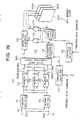
- the color-ghost elimination circuit is composed of, as illustrated in Fig. 15, a first ghost elimination portion 300A and a second ghost elimination portion 300B which is connected in serial to the former. These portions have an identical constitution. Therefore, only one of them is described below.
- the color-ghost elimination process is performed not only in the main-soanning direction (horizontal scanning direction), but the sub-scanning direction (vertical scanning direction) which corresponds with the rotational direction of the image-carrying member 201.
- the color codes read out from the memories 153 through 155 are sequentially supplied to a 7-bit configured shift register 301, where converted into parallel data.
- the parallel color code data for seven pixels are supplied to a ROM 302 which is for eliminating the ghost in the horizontal direction, where subjected to the ghost elimination process on the pixel-by-pixel basis.
- the ROM 302 stores at least post-ghost elimination color code data which correspond with the number of reference color patterns (16384 color patterns) composed of seven pixels.
- the ROM 302 in addition to the post-ghost elimination color code data, stores all the sets of color code data which respectively constitute a post-estimation color pattern.
- Fig. 14 illustrates, if an original document is black-colored, a specific area erroneously turns red or blue; if an original document is red or blue-colored, a specific area erroneously turns black. Accordingly, based on such a characteristic derived from the nature of color separation map, the color of object pixel is estimated using color information on a corresponding color pattern.
- Fig. 17 shows the contents of some color patterns.
- a pixel in the middle is an object pixel which is subjected to the color-ghost elimination process, whereby the object pixel is modified and outputted as listed in this figure.
- the color code data is latched with a latch circuit 303.
- the density data outputted from the memories 153 through 155 are supplied to latch circuit 306 through shift register 305 for timing adjustment, and then the data transfer condition is so set as to serially transfer the density data following the color code data.
- the density data outputted from the memories 153 through 155 are supplied to density correction circuit 350 for the main-scanning direction, via a 5-bit configured shift register 305 for timing adjustment.
- the density correction circuit 350 comprises a ROM 351 which stores density correction data and a comparator circuit 352 for color code data.
- the case which requires the density correction is a case where the pre-color-ghost elimination color code data differs from the post-color-ghost elimination color code data.
- the color code data of an object pixel being supplied to the ROM 303 as well as the color code data outputted from the ROM 302 are supplied to the comparator circuit 352, where whether or not both the color code data accord with each other is detected.
- the density data being outputted from the ROM 351 is selected.
- the post-correction density data is. outputted.
- black pixels converted from red or blue pixels are the pixels on the edge portion.
- the density values of these pixels are shifted toward black side and higher level, in order to prevent the edge portion from becoming an exoessively fine line and to eliminate ruggedness in the black edge portion.
- correction should be made so that an address corresponding with the luminance level become smaller.
- the satisfactory degree of correction is one to three addresses.
- the designed corrected level is reverse to the above correction example.
- level the level of post-correction color should be varied is determined by referring both the color code data outputted from the ROM 302 and the pre-correction density data.
- the density data having been subjected to the density correction is supplied to a latch circuit 306 where data transfer timing is determined so that the density data is transferred serially following the color code data.
- the color code data as well as density data are supplied to a group of line memories 310 in the next stage.
- the group of line memories 310 are provided to eliminate a color-ghost in the vertical direction by using the image data for seven lines.
- the group of line memories include eight lines; this is because an extran one line capacity is necessary to allow real time ghost elimination.
- the color code data and density data for eight lines are separated in a group of gate circuits 320 in the next stage.
- the group of gate circuits 320 include gate circuits 321 through 328 which correspond with the line memories 311 through 318.
- the data for eight line memories converted into parallel data by the group of line memories 310 are respectively separated into the color code data and density data by the group of gate circuits 320, thereby the separated color code data is supplied to a data selection circuit 320, which selects color code data, necessary for color-ghost elimination, of seven line memories among eight line memories.
- a data selection circuit 320 which selects color code data, necessary for color-ghost elimination, of seven line memories among eight line memories.
- the color code data of seven line memories are supplied to a following ROM 340 for eliminating a ghost in the vertical direction, thereby the color-ghost in the vertical direction is eliminated.
- the color code data are latched by a latch circuit 341.
- the density data having been separated by the group of gate circuits 320 is, via a density correction circuit 360 for vertical direction, supplied to a latch circuit 342 which outputs the density data after aligning it for timing with the color code data.
- the ROM 340 also stores estimated color code data which correspond with the number of color patterns (16384 patterns) similar to those mentioned previously.
- the density correction circuit 360 has a constitution similar to the density correction circuit 350 for the horizontal direction, and comprises a density correction ROM 361 for the vertical direction and a comparator circuit 362. This density correction circuit 360 performs density correction with pixels having been subjected to the color-ghost elimination.
- the density correction in the vertical direction is identical with the density correction in the horizontal direction, and is not specifically described.
- Fig. 19 illustrates an apparatus according to the invention, wherein the density data is ternary-coded.
- indicating a ternary-coded data requires at least two bits.
- the color code includes a white color code; this feature allows ternary-coded data to be indicated using one bit.
- a level "H” is regarded as a ternary level; a level “L” is regarded as a binary level.
- a binary-code is positively differentiated from a ternary code by one bit data.
- a color code requires two bits, as is in the previously mentioned case.
- data for one pixel is expressed with three bids including a color code.
- a stored data processing circuit 170 has a configuration shown in Fig. 19.
- the ternary-coded data P1 as well as the binary-coded data P2 are also supplied to a NOR circuit 178, thereby an output from the NOR circuit 178 controls a white code generator 174.
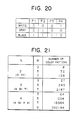
- Fig. 20 The correlation among data P1 through P4 is shown in Fig. 20. Though these data are in fact chromatic color information, this table lists, for convenience of description, the examples, where ternary-coded levels represents luminance information for three achromatic colors (whiet, black and grey).
- a white level corresponds with the level of P4, "H". Accordingly, a white code is obtained from the white code generator 174, in a manner identical with that in Fig. 12. In this course, the level of P3 is "L”.
- the levels of P4 and P3 are “L”s; an inputted color code is unchangingly stored in the memory planes 160a and 160b. Accordingly, the level of the lower code in the color code remains at "L”.
- the level of P3 is "H” and the level of P4 is "L”; the color code is unchangingly stored in the memory planes 160a and 160b. Accordingly, the level of the lower code in the color code is "H”. This feature clearly indicates the black level is a ternary-coded level.
- Such a color image processing apparatus too has a color-ghost elimination circuit 300, whereby color code data as well as density data are individually subjected to the ghost elimination process, as mentioned already.
- the ghost elimination is performed twice using the first and second ghost-elimination portions 300A and 300B.
- the ghost-elimination may be repeated n times continually.
- an original color image is first separated into a plurality of color signals, whereby the color-ghost elimination is repeated continually using a smaller number of color patterns.
- a ROM having a much smaller capacity may serve the ghost-elimination purpose, and which realizes a highly cost effective color image processing apparatus.
- a fine line is not reproduced as an excessively fine line, and an edge portion is free from ruggedness, because not only color code data but density data are corrected in compliance with the status of color-ghost.
- This feature ensures an improved image quality.
- Such a type of density processing is important processing, since most documents are written in black characters and reproducing black color is an outstanding criterion.
- original image data is separated into color code data and density data.
- This arrangement enables single circuitry perform image processing such as enlarging or reducing operation following the above image separation process.
- the color-ghost elimination was performed after the binary-coding step; it was necessary that an enlarging or reducing process be performed per individual color.
- the data of one pixel is first separated into color code data and density data, both of which are next individually stored in a specific memory, and finally stored in a recording device in the form of stored data.
- the storing device stores both the color code data and multi-value-coded data (binary-coded data or ternary-coded data).
- the memory capacity required for an external storage device is much smaller than a conventional device.
- the effect of the invention is more apparent with an increased number of independent colors into which original image is separated, because the memory capacity is more effectively utilized especially in regard to an increased number of independent color signals.
Landscapes
- Engineering & Computer Science (AREA)
- Multimedia (AREA)
- Signal Processing (AREA)
- Facsimile Image Signal Circuits (AREA)
- Color Image Communication Systems (AREA)
- Color Electrophotography (AREA)
Applications Claiming Priority (4)
| Application Number | Priority Date | Filing Date | Title |
|---|---|---|---|
| JP61288313A JPS63141457A (ja) | 1986-12-03 | 1986-12-03 | カラ−画像処理装置 |
| JP61288311A JP2607489B2 (ja) | 1986-12-03 | 1986-12-03 | カラー画像処理装置 |
| JP288313/86 | 1986-12-03 | ||
| JP288311/86 | 1986-12-03 |
Publications (3)
| Publication Number | Publication Date |
|---|---|
| EP0270090A2 true EP0270090A2 (fr) | 1988-06-08 |
| EP0270090A3 EP0270090A3 (en) | 1990-02-28 |
| EP0270090B1 EP0270090B1 (fr) | 1993-09-08 |
Family
ID=26557119
Family Applications (1)
| Application Number | Title | Priority Date | Filing Date |
|---|---|---|---|
| EP19870117814 Expired - Lifetime EP0270090B1 (fr) | 1986-12-03 | 1987-12-02 | Appareil de traitement d'images en couleurs |
Country Status (2)
| Country | Link |
|---|---|
| EP (1) | EP0270090B1 (fr) |
| DE (1) | DE3787351T2 (fr) |
Cited By (15)
| Publication number | Priority date | Publication date | Assignee | Title |
|---|---|---|---|---|
| EP0251278A2 (fr) * | 1986-06-30 | 1988-01-07 | Konica Corporation | Procédé de traitement d'images et appareil à cet effet |
| EP0348145A1 (fr) * | 1988-06-20 | 1989-12-27 | Canon Kabushiki Kaisha | Appareil de formation et de traitement d'images |
| EP0350919A2 (fr) * | 1988-07-15 | 1990-01-17 | Konica Corporation | Appareil de production d'images à couleurs |
| EP0388877A2 (fr) * | 1989-03-22 | 1990-09-26 | Konica Corporation | Appareil de traitement d'image couleur muni de moyens de discrimination d'image |
| EP0395032A2 (fr) * | 1989-04-28 | 1990-10-31 | Konica Corporation | Appareil de traitement d'images en couleurs |
| US4969051A (en) * | 1988-04-14 | 1990-11-06 | Ricoh Company, Ltd. | Image processing apparatus |
| US7551326B2 (en) | 2004-09-30 | 2009-06-23 | Konica Minolta Business Technologies, Inc. | Image reading apparatus for detecting noise in image data |
| US7675657B2 (en) | 2004-09-30 | 2010-03-09 | Konica Minolta Business Technologies, Inc. | Image reading apparatus for detecting noise in image data |
| US7675656B2 (en) | 2004-09-30 | 2010-03-09 | Konica Minolta Business Technologies, Inc. | Image reading apparatus for detecting noise in image data |
| US7697175B2 (en) | 2004-09-30 | 2010-04-13 | Konica Minolta Business Technologies, Inc. | Image reading apparatus capable of detecting noise |
| US7710617B2 (en) | 2004-09-30 | 2010-05-04 | Konica Minolta Business Technologies, Inc. | Image reading apparatus capable of detecting noise |
| US7710618B2 (en) | 2004-09-30 | 2010-05-04 | Konica Minolta Business Technologies, Inc. | Image reading apparatus for detecting noise in image data |
| US7719731B2 (en) | 2004-09-30 | 2010-05-18 | Konica Minolta Business Technologies, Inc. | Image reading apparatus correcting noise in image data |
| US7782506B2 (en) | 2004-11-10 | 2010-08-24 | Konica Minolta Business Technologies, Inc. | Image reading apparatus capable of detecting noise |
| US7839545B2 (en) | 2004-09-30 | 2010-11-23 | Konica Minolta Business Technologies, Inc. | Image reading apparatus correcting noise in image data |
Citations (4)
| Publication number | Priority date | Publication date | Assignee | Title |
|---|---|---|---|---|
| JPS56166666A (en) * | 1980-05-28 | 1981-12-21 | Ricoh Co Ltd | Color picture processor |
| JPS60160774A (ja) * | 1984-01-31 | 1985-08-22 | Fuji Xerox Co Ltd | 2色原稿読み取り装置 |
| EP0251278A2 (fr) * | 1986-06-30 | 1988-01-07 | Konica Corporation | Procédé de traitement d'images et appareil à cet effet |
| EP0270087A2 (fr) * | 1986-12-03 | 1988-06-08 | Konica Corporation | Appareil pour le traitement d'images en couleurs |
-
1987
- 1987-12-02 DE DE19873787351 patent/DE3787351T2/de not_active Expired - Fee Related
- 1987-12-02 EP EP19870117814 patent/EP0270090B1/fr not_active Expired - Lifetime
Patent Citations (4)
| Publication number | Priority date | Publication date | Assignee | Title |
|---|---|---|---|---|
| JPS56166666A (en) * | 1980-05-28 | 1981-12-21 | Ricoh Co Ltd | Color picture processor |
| JPS60160774A (ja) * | 1984-01-31 | 1985-08-22 | Fuji Xerox Co Ltd | 2色原稿読み取り装置 |
| EP0251278A2 (fr) * | 1986-06-30 | 1988-01-07 | Konica Corporation | Procédé de traitement d'images et appareil à cet effet |
| EP0270087A2 (fr) * | 1986-12-03 | 1988-06-08 | Konica Corporation | Appareil pour le traitement d'images en couleurs |
Non-Patent Citations (2)
| Title |
|---|
| PATENT ABSTRACTS OF JAPAN, vol. 6, no. 52 (E-100)[930], 7th April 1982; & JP-A-56 166 666 (RICOH K.K.) * |
| PATENT ABSTRACTS OF JAPAN, vol. 9, no. 382 (E-369), 24th December 1985, page 42 E 369; & JP-A-60 160 774 (FUJI XEROX K.K.) 22-08-1985 * |
Cited By (24)
| Publication number | Priority date | Publication date | Assignee | Title |
|---|---|---|---|---|
| EP0251278A3 (en) * | 1986-06-30 | 1990-02-28 | Konishiroku Photo Industry Co. Ltd. | Image processing method and apparatus therefor |
| EP0251278A2 (fr) * | 1986-06-30 | 1988-01-07 | Konica Corporation | Procédé de traitement d'images et appareil à cet effet |
| US4980758A (en) * | 1986-06-30 | 1990-12-25 | Konica Corporation | Image processing technique for processing digital color image information |
| US4969051A (en) * | 1988-04-14 | 1990-11-06 | Ricoh Company, Ltd. | Image processing apparatus |
| EP0348145A1 (fr) * | 1988-06-20 | 1989-12-27 | Canon Kabushiki Kaisha | Appareil de formation et de traitement d'images |
| US5031034A (en) * | 1988-06-20 | 1991-07-09 | Canon Kabushiki Kaisha | Image forming and processing apparatus with identification of character portions of images |
| US5130791A (en) * | 1988-07-15 | 1992-07-14 | Konica Corporation | Color image processing apparatus |
| EP0350919A2 (fr) * | 1988-07-15 | 1990-01-17 | Konica Corporation | Appareil de production d'images à couleurs |
| EP0350919A3 (en) * | 1988-07-15 | 1990-09-26 | Konica Corporation | Color image processing apparatus |
| EP0388877A2 (fr) * | 1989-03-22 | 1990-09-26 | Konica Corporation | Appareil de traitement d'image couleur muni de moyens de discrimination d'image |
| EP0388877A3 (fr) * | 1989-03-22 | 1992-09-02 | Konica Corporation | Appareil de traitement d'image couleur muni de moyens de discrimination d'image |
| EP0395032A2 (fr) * | 1989-04-28 | 1990-10-31 | Konica Corporation | Appareil de traitement d'images en couleurs |
| EP0395032A3 (fr) * | 1989-04-28 | 1991-04-03 | Konica Corporation | Appareil de traitement d'images en couleurs |
| US7551326B2 (en) | 2004-09-30 | 2009-06-23 | Konica Minolta Business Technologies, Inc. | Image reading apparatus for detecting noise in image data |
| US7675657B2 (en) | 2004-09-30 | 2010-03-09 | Konica Minolta Business Technologies, Inc. | Image reading apparatus for detecting noise in image data |
| US7675656B2 (en) | 2004-09-30 | 2010-03-09 | Konica Minolta Business Technologies, Inc. | Image reading apparatus for detecting noise in image data |
| US7697175B2 (en) | 2004-09-30 | 2010-04-13 | Konica Minolta Business Technologies, Inc. | Image reading apparatus capable of detecting noise |
| US7710617B2 (en) | 2004-09-30 | 2010-05-04 | Konica Minolta Business Technologies, Inc. | Image reading apparatus capable of detecting noise |
| US7710618B2 (en) | 2004-09-30 | 2010-05-04 | Konica Minolta Business Technologies, Inc. | Image reading apparatus for detecting noise in image data |
| US7719731B2 (en) | 2004-09-30 | 2010-05-18 | Konica Minolta Business Technologies, Inc. | Image reading apparatus correcting noise in image data |
| US7839545B2 (en) | 2004-09-30 | 2010-11-23 | Konica Minolta Business Technologies, Inc. | Image reading apparatus correcting noise in image data |
| US7969627B2 (en) | 2004-09-30 | 2011-06-28 | Konica Minolta Business Technologies, Inc. | Image reading apparatus for detecting noise in image data |
| US7973986B2 (en) | 2004-09-30 | 2011-07-05 | Konica Minolta Business Technologies, Inc. | Image reading apparatus for detecting noise in image data |
| US7782506B2 (en) | 2004-11-10 | 2010-08-24 | Konica Minolta Business Technologies, Inc. | Image reading apparatus capable of detecting noise |
Also Published As
| Publication number | Publication date |
|---|---|
| DE3787351D1 (de) | 1993-10-14 |
| DE3787351T2 (de) | 1994-01-13 |
| EP0270090A3 (en) | 1990-02-28 |
| EP0270090B1 (fr) | 1993-09-08 |
Similar Documents
| Publication | Publication Date | Title |
|---|---|---|
| US4841361A (en) | Color image processing apparatus | |
| US4980760A (en) | Image processing apparatus | |
| US4667250A (en) | Halftone digital image processing device | |
| US5721628A (en) | Color image processing apparatus | |
| EP0270090B1 (fr) | Appareil de traitement d'images en couleurs | |
| JP2892037B2 (ja) | カラー画像処理装置 | |
| US4878110A (en) | Color image processing apparatus which accurately registers multiple color images by counting pulses from a timer reset by a drum index signal | |
| US5208663A (en) | Color image processing apparatus provided with an image discrimination means | |
| US5418602A (en) | Image processing with anti-forgery provision | |
| JPS63141441A (ja) | カラ−画像処理装置 | |
| US5119184A (en) | Color image processing apparatus with digital color signal compression means | |
| JP2607489B2 (ja) | カラー画像処理装置 | |
| JP2683164B2 (ja) | カラ−画像形成装置 | |
| US5418618A (en) | Tone processing method for forming a halftone image | |
| US5220416A (en) | Color image processing apparatus | |
| JP2621856B2 (ja) | デジタルカラー画像再生処理方法および装置 | |
| JPS62170A (ja) | デジタルカラ−画像処理装置 | |
| JPS61196668A (ja) | デジタルカラ−複写機 | |
| EP0508123A1 (fr) | Appareil de traitement d'image | |
| JP2887483B2 (ja) | 多色画情報生成装置及びこれを用いた画像処理装置 | |
| JP2549627B2 (ja) | デジタルカラ−画像再生処理方法および装置 | |
| JP2751163B2 (ja) | カラー画像処理装置 | |
| JPS63193771A (ja) | カラ−画像処理装置 | |
| JP2773079B2 (ja) | カラー画像処理装置 | |
| JPS61288565A (ja) | 中間調デジタル画像処理装置 |
Legal Events
| Date | Code | Title | Description |
|---|---|---|---|
| PUAI | Public reference made under article 153(3) epc to a published international application that has entered the european phase |
Free format text: ORIGINAL CODE: 0009012 |
|
| AK | Designated contracting states |
Kind code of ref document: A2 Designated state(s): DE FR GB IT NL SE |
|
| PUAL | Search report despatched |
Free format text: ORIGINAL CODE: 0009013 |
|
| AK | Designated contracting states |
Kind code of ref document: A3 Designated state(s): DE FR GB IT NL SE |
|
| 17P | Request for examination filed |
Effective date: 19900807 |
|
| 17Q | First examination report despatched |
Effective date: 19920330 |
|
| GRAA | (expected) grant |
Free format text: ORIGINAL CODE: 0009210 |
|
| AK | Designated contracting states |
Kind code of ref document: B1 Designated state(s): DE FR GB IT NL SE |
|
| PG25 | Lapsed in a contracting state [announced via postgrant information from national office to epo] |
Ref country code: IT Free format text: LAPSE BECAUSE OF FAILURE TO SUBMIT A TRANSLATION OF THE DESCRIPTION OR TO PAY THE FEE WITHIN THE PRE;WARNING: LAPSES OF ITALIAN PATENTS WITH EFFECTIVE DATE BEFORE 2007 MAY HAVE OCCURRED AT ANY TIME BEFORE 2007. THE CORRECT EFFECTIVE DATE MAY BE DIFFERENT FROM THE ONE RECORDED.SCRIBED TIME-LIMIT Effective date: 19930908 Ref country code: NL Effective date: 19930908 Ref country code: FR Effective date: 19930908 Ref country code: SE Effective date: 19930908 |
|
| REF | Corresponds to: |
Ref document number: 3787351 Country of ref document: DE Date of ref document: 19931014 |
|
| EN | Fr: translation not filed | ||
| NLV1 | Nl: lapsed or annulled due to failure to fulfill the requirements of art. 29p and 29m of the patents act | ||
| PLBE | No opposition filed within time limit |
Free format text: ORIGINAL CODE: 0009261 |
|
| STAA | Information on the status of an ep patent application or granted ep patent |
Free format text: STATUS: NO OPPOSITION FILED WITHIN TIME LIMIT |
|
| 26N | No opposition filed | ||
| PGFP | Annual fee paid to national office [announced via postgrant information from national office to epo] |
Ref country code: GB Payment date: 19951123 Year of fee payment: 9 |
|
| PGFP | Annual fee paid to national office [announced via postgrant information from national office to epo] |
Ref country code: DE Payment date: 19951214 Year of fee payment: 9 |
|
| PG25 | Lapsed in a contracting state [announced via postgrant information from national office to epo] |
Ref country code: GB Effective date: 19961202 |
|
| GBPC | Gb: european patent ceased through non-payment of renewal fee |
Effective date: 19961202 |
|
| PG25 | Lapsed in a contracting state [announced via postgrant information from national office to epo] |
Ref country code: DE Effective date: 19970902 |