EP0267667A2 - Laser à résonateur distribué - Google Patents
Laser à résonateur distribué Download PDFInfo
- Publication number
- EP0267667A2 EP0267667A2 EP87305603A EP87305603A EP0267667A2 EP 0267667 A2 EP0267667 A2 EP 0267667A2 EP 87305603 A EP87305603 A EP 87305603A EP 87305603 A EP87305603 A EP 87305603A EP 0267667 A2 EP0267667 A2 EP 0267667A2
- Authority
- EP
- European Patent Office
- Prior art keywords
- laser
- dfb
- distributed feedback
- contacts
- electrode structure
- Prior art date
- Legal status (The legal status is an assumption and is not a legal conclusion. Google has not performed a legal analysis and makes no representation as to the accuracy of the status listed.)
- Withdrawn
Links
Images


Classifications
-
- H—ELECTRICITY
- H01—ELECTRIC ELEMENTS
- H01S—DEVICES USING THE PROCESS OF LIGHT AMPLIFICATION BY STIMULATED EMISSION OF RADIATION [LASER] TO AMPLIFY OR GENERATE LIGHT; DEVICES USING STIMULATED EMISSION OF ELECTROMAGNETIC RADIATION IN WAVE RANGES OTHER THAN OPTICAL
- H01S5/00—Semiconductor lasers
- H01S5/06—Arrangements for controlling the laser output parameters, e.g. by operating on the active medium
- H01S5/062—Arrangements for controlling the laser output parameters, e.g. by operating on the active medium by varying the potential of the electrodes
- H01S5/0625—Arrangements for controlling the laser output parameters, e.g. by operating on the active medium by varying the potential of the electrodes in multi-section lasers
- H01S5/06255—Controlling the frequency of the radiation
- H01S5/06258—Controlling the frequency of the radiation with DFB-structure
-
- H—ELECTRICITY
- H01—ELECTRIC ELEMENTS
- H01S—DEVICES USING THE PROCESS OF LIGHT AMPLIFICATION BY STIMULATED EMISSION OF RADIATION [LASER] TO AMPLIFY OR GENERATE LIGHT; DEVICES USING STIMULATED EMISSION OF ELECTROMAGNETIC RADIATION IN WAVE RANGES OTHER THAN OPTICAL
- H01S5/00—Semiconductor lasers
- H01S5/10—Construction or shape of the optical resonator, e.g. extended or external cavity, coupled cavities, bent-guide, varying width, thickness or composition of the active region
- H01S5/12—Construction or shape of the optical resonator, e.g. extended or external cavity, coupled cavities, bent-guide, varying width, thickness or composition of the active region the resonator having a periodic structure, e.g. in distributed feedback [DFB] lasers
-
- H—ELECTRICITY
- H01—ELECTRIC ELEMENTS
- H01S—DEVICES USING THE PROCESS OF LIGHT AMPLIFICATION BY STIMULATED EMISSION OF RADIATION [LASER] TO AMPLIFY OR GENERATE LIGHT; DEVICES USING STIMULATED EMISSION OF ELECTROMAGNETIC RADIATION IN WAVE RANGES OTHER THAN OPTICAL
- H01S5/00—Semiconductor lasers
- H01S5/04—Processes or apparatus for excitation, e.g. pumping, e.g. by electron beams
- H01S5/042—Electrical excitation ; Circuits therefor
- H01S5/0425—Electrodes, e.g. characterised by the structure
- H01S5/04256—Electrodes, e.g. characterised by the structure characterised by the configuration
-
- H—ELECTRICITY
- H01—ELECTRIC ELEMENTS
- H01S—DEVICES USING THE PROCESS OF LIGHT AMPLIFICATION BY STIMULATED EMISSION OF RADIATION [LASER] TO AMPLIFY OR GENERATE LIGHT; DEVICES USING STIMULATED EMISSION OF ELECTROMAGNETIC RADIATION IN WAVE RANGES OTHER THAN OPTICAL
- H01S5/00—Semiconductor lasers
- H01S5/06—Arrangements for controlling the laser output parameters, e.g. by operating on the active medium
- H01S5/062—Arrangements for controlling the laser output parameters, e.g. by operating on the active medium by varying the potential of the electrodes
- H01S5/0625—Arrangements for controlling the laser output parameters, e.g. by operating on the active medium by varying the potential of the electrodes in multi-section lasers
- H01S5/06255—Controlling the frequency of the radiation
-
- H—ELECTRICITY
- H01—ELECTRIC ELEMENTS
- H01S—DEVICES USING THE PROCESS OF LIGHT AMPLIFICATION BY STIMULATED EMISSION OF RADIATION [LASER] TO AMPLIFY OR GENERATE LIGHT; DEVICES USING STIMULATED EMISSION OF ELECTROMAGNETIC RADIATION IN WAVE RANGES OTHER THAN OPTICAL
- H01S5/00—Semiconductor lasers
- H01S5/10—Construction or shape of the optical resonator, e.g. extended or external cavity, coupled cavities, bent-guide, varying width, thickness or composition of the active region
- H01S5/12—Construction or shape of the optical resonator, e.g. extended or external cavity, coupled cavities, bent-guide, varying width, thickness or composition of the active region the resonator having a periodic structure, e.g. in distributed feedback [DFB] lasers
- H01S5/1206—Construction or shape of the optical resonator, e.g. extended or external cavity, coupled cavities, bent-guide, varying width, thickness or composition of the active region the resonator having a periodic structure, e.g. in distributed feedback [DFB] lasers having a non constant or multiplicity of periods
- H01S5/1215—Multiplicity of periods
Definitions
- This invention relates to distributed feedback (DFB) lasers.
- DFB lasers with nominally identical gratings and waveguides that are derived from the same wafer can typically be expected to have a device to device wavelength scatter of up to about 1nm.
- a tuning range of 1nm is therefore required so that all devices from one wafer can be matched to a fixed local oscillator frequency.
- a greater tuning range is desirable, preferably about 5nm, though for a number of applications about 2nm should suffice.
- One method of tuning the output of a DFB laser is described in European Patent Application Specification No. EP 0 169 567 A2 to which attention is directed.
- the method described therein involves a construction of laser chip in which distributed feedback is provided along only a portion of the whole length of the optical cavity within the chip, that portion extending from one end. At the other end a highly reflecting facet is provided.
- the emission wavelength is tuneable over a restricted range by adjusting the current drive applied to the region of the optical cavity extending between the highly reflecting facet and the distributed feedback region. Adjustment of this drive affects the refractive index, thereby affecting the phase of light reflected back into the distributed feedback region, and hence the frequency of laser emission.
- the present invention is concerned with an alternative method of tuning DFB lasers embodiments of which are believed intrinsically capable of a relatively wider tuning range.
- a distributed feedback (DFB) laser provided with three or more electrodes disposed such that by control of the relative current flow through said electrodes the injected current profile in the distributed feedback region of the laser is adjustable to vary the frequency of the laser output independently of its optical amplitude.
- DFB distributed feedback
- DFB laser Various different structures of DFB laser are possible, thus one known structure has its diffraction grating formed in a layer grown before the growth of the active layer, while in another the grating is formed in a layer grown after the growth of the active layer.
- the present invention will be exemplified in particular with reference to a DFB laser structure of this second kind, but it should be clearly understood that the invention is not limited in its application solely to this kind of DFB laser structure.
- five epitaxial layers 11 to 15 are grown upon an n-type InP substrate 10.
- Layer 11 is an n-type buffer layer of InP.
- layer 12 which is of quaternary material (InGaAsP) having a composition providing an emission wavelength in the wavelength range from 1.3 to 1.6 ⁇ m.
- Layer 13 is a layer variously referred to as the anti-meltback layer or as the guide layer, and is formed of p-type InGaAsP of greater band gap than that of active layer 12.
- Epitaxial growth is temporarily halted at this stage in order to form a diffraction grating 16 in its surface before growth is recommenced to form layer 14, which is of p-type InP and constitutes the p-confining layer, and then to form layer 15 which is a capping layer of InGaAsP or InGaAs.
- channels 17 are etched which descend to the anti-meltback layer 13 and define an intervening stripe 18. These channels 17 are coated or filled with electrically insulating passivation 19.
- a contact layer 20 is also formed on the under-surface of substrate 10 to form a counter-electrode.
- the arrangement of contacts on the capping layer 15 of Figure 1 is such as to provide a longitudinally divided electrode structure with three parallel stripe contacts 24, 25 and 26 registering with the stripe 18 of Figure 1 (defined by its two channels 17).
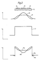
- the material of the stripe 18 has a higher refractive index than that of the material filling the channels 17, and thus the channels co-operate with the stripe to provide a built-in waveguiding structure with an index profile as depicted at 27 in Figure 2.
- This index profile forms a built-in waveguide for guiding the laser light within the body of the laser. This profile is however modified by the presence of carriers which have the effect of depressing the refractive index.
- the effect of the distributed feedback grating upon emission wavelength of the laser is controlled not essentially by the pitch of that grating expressed in terms of physical distance, but rather it is controlled by the pitch expressed in terms of optical path length (the product of physical distance with effective refractive index). Therefore any change of carrier density that produces a change in effective refractive index seen by the laser light will produce an attendant change in emission wavelength.
- the provision of the three contacts enables some control over the profile of the injected current. If the current is injected solely through the central one of the three contacts, contact 25, a relatively sharply peaked carrier density profile is produced, as exemplified for instance by curve 28. This modifies the built-in index profile to result in the index profile given by curve 28a. At any particular level of current drive there is produced a particular effective refractive index of the guide and hence a particular wavelength of emission. A change in drive produces a change in carrier density and hence a change in emission wavelength. If however, the current is injected equally through all three contacts 24, 25 and 26, or even preferentially into the outer contacts 24 and 26, a flatter carrier density profile is provided, as exemplified by curve 29. This flatter curve is less disruptive than curve 28 of the waveguiding provided by the built-in waveguide profile 27, and produces the index profile of curve 29a, with the result that the efficiency of laser light generation is greater.
- the injected current drive level that produces the same effective refractive index as produced by current injection solely through contact 26, produces a greater optical output, but at the same wavelength.
- the same type of adjustment of current drive may be employed to adjust the emission wavelength provided at any given optical output level.
- a feature of the laser of Figure 2 is that it does not suffer from the same type of tuning constraints as the phase tuneable laser of EP 0 169 567 in that in the phase tuneable laser the tuning range is intrinsically limited by mode-hopping considerations.
- the natural resonance condition of the distributed feedback portion of the laser is in effect perturbed by the resonance characteristics of the phase-tuning portion. This contrasts with the laser described with particular reference to the present Figure 2 in which tuning is instead achieved by adjustment of natural resonance condition presented by the distributed feedback structure.
- Figure 3 depicts a modified version which has two contacts 31 and 32 in place of the three contacts 24, 25 and 26.
- symmetric current injection produces an injection carrier density profile of the form given by curve 33, while an asymmetric drive with more current injected into contact 31 produces a profile of the form given by curve 34, and is associated with lower efficiency of laser light generation than the symmetric drive state.
- the lasers of Figures 2 and 3 have involved the longitudinal division of the top electrode structure, whereas in the laser of Figure 4 the electrode structure has been divided transversely to provide two contacts 40 and 41.
- Underlying contact 40 the diffraction grating 16 ( Figure 1) is formed with a certain pitch indicated by the lines 42, while the corresponding portion of the grating 16 underlying contact 41 is formed with a slightly different pitch indicated by the lines 43. (In the drawing the difference in pitch has been greatly exaggerated; in actuality the difference will typically not be more than about 0.05%.)
- This structure may be considered as comprising two coupled resonators.
- the grating can be graded in pitch from end to end in a single chirp.
- one characteristic of the laser of Figure 4 is that when tuning from one end of the tuning range to the other the concentration of gain is also shifted from one end to the other, with the result that the distribution of power output between the two ends is also changed.
- This characteristic is avoided in the laser of Figure 5 by virtue of its symmetrical layout and drive.
- This laser is divided transversely to provide three contacts 50, 51 and 52. The arrangement of these contacts, and the grading of the pitch of the distributed feedback grating, as represented by lines 54, are both symmetrical about a centre line 55.
- Figure 6 depicts a further alternative construction of laser with a transversely divided electrode structure.
- This employs four contacts 60, 61, 62 and 63 in association with an antisymmetric chirp in the pitch of the underlying grating 64.
- Differential drive is effected between contacts 60 and 62 which are common to and between contacts 61 and 63, which are likewise commoned.
- the chirp (with grading greatly exaggerated) extending beneath contacts 60 and 61 up to the centre line 65 is repated under contacts 62 and 63.
- a longitudinally divided electrode structure is employed to enable the shape of the current profile to be varied so as to alter the lasing efficiency of the device, and hence permit independent control of output power and wavelength.
- the laser of Figure 7 similarly employs a longitudinally divided electrode structure with electrodes 70, 71 and 72, but in this instance the division of the electrodes is provided in order to allow the centre-of-gravity of the injected current, and consequently the optical filament, to be shifted laterally across a region 73 where the propagation constants of the laser change either due to a change in composition which produces a change of refractive index, or due to a change in thickness of at least one of layers 11, 12 or 13 (the buffer layer, the active layer, or the anti-meltback layer).
- the centre-of-gravity is slowly transferred from one side of region 73 to the other so the wavelength is progressively shifted from a value determined primarily by the propagation constants of the one side to value determined primarily by the propagation constants
- the laser of Figure 8 similarly relies upon the effects of laterally shifting the centre of gravity of the injected current by means of adjustment of the current between the three electrodes 80, 81 and 82 of a longitudinally divided electrode structure on the capping layer 15 of Figure 1.
- this lateral shift produces a wavelength change because the grating lines 84 are radially arranged instead of being parallel to each other.
- the waveguide in this case can be straight or it may be curved. With typical waveguide parameters a curvature down to a radius of about 300 ⁇ m is satisfactory.
Applications Claiming Priority (2)
| Application Number | Priority Date | Filing Date | Title |
|---|---|---|---|
| GB8626730A GB2197531B (en) | 1986-11-08 | 1986-11-08 | Distributed feedback laser |
| GB8626730 | 1986-11-08 |
Publications (2)
| Publication Number | Publication Date |
|---|---|
| EP0267667A2 true EP0267667A2 (fr) | 1988-05-18 |
| EP0267667A3 EP0267667A3 (fr) | 1988-11-09 |
Family
ID=10607023
Family Applications (1)
| Application Number | Title | Priority Date | Filing Date |
|---|---|---|---|
| EP87305603A Withdrawn EP0267667A3 (fr) | 1986-11-08 | 1987-06-24 | Laser à résonateur distribué |
Country Status (4)
| Country | Link |
|---|---|
| US (1) | US4813054A (fr) |
| EP (1) | EP0267667A3 (fr) |
| JP (1) | JPS63128691A (fr) |
| GB (1) | GB2197531B (fr) |
Cited By (7)
| Publication number | Priority date | Publication date | Assignee | Title |
|---|---|---|---|---|
| FR2644892A1 (fr) * | 1989-03-23 | 1990-09-28 | Anritsu Corp | Appareil de detection de gaz par absorption lumineuse |
| EP0525622A2 (fr) * | 1991-07-22 | 1993-02-03 | Eastman Kodak Company | Diode laser à semi-conducteur à guidage par indice avec les deux contacts sur la même surface |
| EP0559192A2 (fr) * | 1992-03-06 | 1993-09-08 | Nippon Telegraph And Telephone Corporation | Réflecteur distribué et laser à semi-conducteur à longeur d'onde accordable |
| EP0601989A1 (fr) * | 1992-12-09 | 1994-06-15 | Telefonaktiebolaget Lm Ericsson | Dispositif de filtrage à commande électrique |
| DE4334525A1 (de) * | 1993-10-09 | 1995-04-13 | Deutsche Bundespost Telekom | Optoelektronisches Bauelement mit verteilter Rückkopplung und variierbarem Kopplungskoeffizienten |
| EP1703603A1 (fr) | 2005-03-17 | 2006-09-20 | Fujitsu Limited | Laser accordable |
| EP1304780B1 (fr) * | 2001-10-18 | 2017-05-10 | nanoplus Nanosystems and Technologies GmbH | Laser à semiconducteur accordable sur bande large |
Families Citing this family (68)
| Publication number | Priority date | Publication date | Assignee | Title |
|---|---|---|---|---|
| US4972352A (en) * | 1988-08-10 | 1990-11-20 | Shildon Limited | Semiconductors lasers |
| JPH0287692A (ja) * | 1988-09-26 | 1990-03-28 | Mitsubishi Electric Corp | 半導体光素子 |
| EP0361399A3 (fr) * | 1988-09-28 | 1990-07-18 | Canon Kabushiki Kaisha | Réseau laser à semi-conducteur contenant des lasers avec des moyens de reflexion présentant des propriétés de sélection de longueur d'onde différentes |
| NL8803080A (nl) * | 1988-12-16 | 1990-07-16 | Philips Nv | Verstembare halfgeleiderdiodelaser met verdeelde reflectie en vervaardigingswijze van een dergelijke halfgeleiderdiodelaser. |
| JPH02207581A (ja) * | 1989-02-07 | 1990-08-17 | Tokyo Inst Of Technol | 波長可変半導体レーザ装置 |
| GB2234632A (en) * | 1989-08-01 | 1991-02-06 | British Telecomm | Distributed feedback laser |
| CA2091302A1 (fr) * | 1992-03-11 | 1993-09-12 | Ichiro Yoshida | Laser a semiconducteur et sa methode de fabrication |
| JP2950302B2 (ja) * | 1997-11-25 | 1999-09-20 | 日本電気株式会社 | 半導体レーザ |
| US7969965B2 (en) * | 1999-04-21 | 2011-06-28 | Lgc Wireless, Inc. | Architecture for signal and power distribution in wireless data network |
| US8379569B2 (en) * | 1999-04-21 | 2013-02-19 | Adc Telecommunications, Inc. | Architecture for signal distribution in wireless data network |
| EP1269776B1 (fr) * | 2000-03-27 | 2009-07-01 | OpenCell Corp. | Système pour diffuser des signaux radio-fréquence multi-protocole |
| ATE382222T1 (de) * | 2000-03-29 | 2008-01-15 | Opencell Corp | Betriebs- und wartungs-architektur für ein verteiltes multiprotokollsystem |
| US6704545B1 (en) * | 2000-07-19 | 2004-03-09 | Adc Telecommunications, Inc. | Point-to-multipoint digital radio frequency transport |
| GB2371920A (en) * | 2001-02-02 | 2002-08-07 | Marconi Caswell Ltd | Sampled Gating Distribiuted Reflector Laser |
| GB2377545A (en) | 2001-07-14 | 2003-01-15 | Marconi Caswell Ltd | Tuneable Laser |
| GB2379084B (en) * | 2001-08-24 | 2006-03-29 | Marconi Caswell Ltd | Surface emitting laser |
| KR100429531B1 (ko) * | 2001-10-12 | 2004-05-03 | 삼성전자주식회사 | 분포귀환형 반도체 레이저 |
| US7184728B2 (en) * | 2002-02-25 | 2007-02-27 | Adc Telecommunications, Inc. | Distributed automatic gain control system |
| GB2385979B (en) * | 2002-02-28 | 2005-10-12 | Bookham Technology Plc | Control for a tunable laser |
| US6831901B2 (en) * | 2002-05-31 | 2004-12-14 | Opencell Corporation | System and method for retransmission of data |
| US8958789B2 (en) * | 2002-12-03 | 2015-02-17 | Adc Telecommunications, Inc. | Distributed digital antenna system |
| US7171244B2 (en) * | 2002-12-03 | 2007-01-30 | Adc Telecommunications, Inc. | Communication system and method with gain control for signals from distributed antennas |
| US7103377B2 (en) * | 2002-12-03 | 2006-09-05 | Adc Telecommunications, Inc. | Small signal threshold and proportional gain distributed digital communications |
| US7593450B2 (en) * | 2005-03-31 | 2009-09-22 | Adc Telecommunications, Inc. | Dynamic frequency hopping |
| US7423988B2 (en) * | 2005-03-31 | 2008-09-09 | Adc Telecommunications, Inc. | Dynamic reconfiguration of resources through page headers |
| US20060222020A1 (en) * | 2005-03-31 | 2006-10-05 | Adc Telecommunications, Inc. | Time start in the forward path |
| US7398106B2 (en) * | 2005-03-31 | 2008-07-08 | Adc Telecommunications, Inc. | Dynamic readjustment of power |
| US7640019B2 (en) * | 2005-03-31 | 2009-12-29 | Adc Telecommunications, Inc. | Dynamic reallocation of bandwidth and modulation protocols |
| US7583735B2 (en) * | 2005-03-31 | 2009-09-01 | Adc Telecommunications, Inc. | Methods and systems for handling underflow and overflow in a software defined radio |
| US20070008939A1 (en) * | 2005-06-10 | 2007-01-11 | Adc Telecommunications, Inc. | Providing wireless coverage into substantially closed environments |
| US7797694B2 (en) * | 2005-09-19 | 2010-09-14 | Adc Telecommunications, Inc. | Mechanism to upgrade system capability without affecting service |
| US20070071450A1 (en) * | 2005-09-29 | 2007-03-29 | Adc Telecommunications, Inc. | Systems and methods for optical power window control |
| US7729620B2 (en) * | 2005-09-29 | 2010-06-01 | Adc Telecommunications, Inc. | Methods and systems for controlling optical power attenuation |
| US7603093B2 (en) * | 2005-12-14 | 2009-10-13 | Adc Telecommunications, Inc. | System and method to monitor broadband radio frequency transport systems |
| US20070195905A1 (en) * | 2006-02-21 | 2007-08-23 | Adc Telecommunications, Inc. | Forward error correction in wideband digital RF transport systems |
| US7610046B2 (en) * | 2006-04-06 | 2009-10-27 | Adc Telecommunications, Inc. | System and method for enhancing the performance of wideband digital RF transport systems |
| US7805073B2 (en) | 2006-04-28 | 2010-09-28 | Adc Telecommunications, Inc. | Systems and methods of optical path protection for distributed antenna systems |
| US7844273B2 (en) * | 2006-07-14 | 2010-11-30 | Lgc Wireless, Inc. | System for and method of for providing dedicated capacity in a cellular network |
| US7848770B2 (en) * | 2006-08-29 | 2010-12-07 | Lgc Wireless, Inc. | Distributed antenna communications system and methods of implementing thereof |
| US7817958B2 (en) * | 2006-12-22 | 2010-10-19 | Lgc Wireless Inc. | System for and method of providing remote coverage area for wireless communications |
| US8583100B2 (en) * | 2007-01-25 | 2013-11-12 | Adc Telecommunications, Inc. | Distributed remote base station system |
| US8737454B2 (en) * | 2007-01-25 | 2014-05-27 | Adc Telecommunications, Inc. | Modular wireless communications platform |
| US20080227441A1 (en) * | 2007-03-12 | 2008-09-18 | Adc Telecommunications, Inc. | Systems and methods for a universal base station |
| US8005050B2 (en) * | 2007-03-23 | 2011-08-23 | Lgc Wireless, Inc. | Localization of a mobile device in distributed antenna communications system |
| US20080240225A1 (en) * | 2007-03-27 | 2008-10-02 | Adc Telecommunications, Inc. | Method and system for enhancing the performance of wideband digital rf transport systems |
| US8457562B2 (en) * | 2007-03-27 | 2013-06-04 | Adc Telecommunications, Inc. | Digitized reverse link monitor |
| US7668153B2 (en) * | 2007-03-27 | 2010-02-23 | Adc Telecommunications, Inc. | Method for data converter sample clock distribution |
| US8010116B2 (en) * | 2007-06-26 | 2011-08-30 | Lgc Wireless, Inc. | Distributed antenna communications system |
| US7948897B2 (en) * | 2007-08-15 | 2011-05-24 | Adc Telecommunications, Inc. | Delay management for distributed communications networks |
| US7974244B2 (en) * | 2007-08-21 | 2011-07-05 | Adc Telecommunications, Inc. | Method and system for reducing uplink noise in wireless communication systems |
| US9112547B2 (en) * | 2007-08-31 | 2015-08-18 | Adc Telecommunications, Inc. | System for and method of configuring distributed antenna communications system |
| US8462661B2 (en) * | 2007-09-21 | 2013-06-11 | Adc Dsl Systems, Inc. | Auto-discovery in a switch |
| CA2714564C (fr) * | 2008-02-08 | 2014-10-28 | Adc Telecommunications, Inc. | Reseau mobile d'entreprise pour fournir un service cellulaire sans fil au moyen d'un spectre radiofrequence autorise et prendre en charge une sonnerie multi-dispositif pour les appels entrants |
| US7961689B2 (en) * | 2008-08-18 | 2011-06-14 | Adc Telecommunications, Inc. | Method and apparatus for determining an end of a subframe in a TDD system |
| US8305993B2 (en) * | 2008-09-30 | 2012-11-06 | Altobridge Limited | Integration of a private cellular system into a unified communications solution |
| US20100080198A1 (en) * | 2008-09-30 | 2010-04-01 | Adc Telecommunications, Inc. | Internet protocol cellular private branch exchange |
| US8165169B2 (en) * | 2008-12-02 | 2012-04-24 | Adc Telecommunications, Inc. | Clock priority chain level systems and methods |
| US20100135674A1 (en) * | 2008-12-02 | 2010-06-03 | Adc Telecommunications, Inc. | Complex optical modulation for real time communication |
| US8184745B2 (en) * | 2008-12-04 | 2012-05-22 | Altobridge Limited | System and method of generating soft bits |
| EP3585019B1 (fr) * | 2009-01-13 | 2023-08-16 | Commscope Technologies LLC | Dispositif de communication permettant de fournir un transport numérique de signaux dans un système d'antenne distribué |
| US8306563B2 (en) * | 2009-01-29 | 2012-11-06 | Adc Telecommunications, Inc. | Method and apparatus for muting a digital link in a distributed antenna system |
| US20100208777A1 (en) * | 2009-02-17 | 2010-08-19 | Adc Telecommunications, Inc. | Distributed antenna system using gigabit ethernet physical layer device |
| US8270522B2 (en) * | 2009-04-13 | 2012-09-18 | Altobridge Limited | Joint channel estimation and modulation detection |
| US8379761B2 (en) * | 2009-04-13 | 2013-02-19 | Altobridge Limited | Smooth modulation switching |
| US9001811B2 (en) * | 2009-05-19 | 2015-04-07 | Adc Telecommunications, Inc. | Method of inserting CDMA beacon pilots in output of distributed remote antenna nodes |
| US8472579B2 (en) | 2010-07-28 | 2013-06-25 | Adc Telecommunications, Inc. | Distributed digital reference clock |
| CN103490280B (zh) * | 2013-09-27 | 2016-01-20 | 中国科学院半导体研究所 | 可调谐分布反馈量子级联激光器阵列器件及其制备方法 |
| CN103545711B (zh) * | 2013-10-22 | 2015-12-30 | 中国科学院半导体研究所 | 分布反馈式激光器及其制备方法 |
Citations (4)
| Publication number | Priority date | Publication date | Assignee | Title |
|---|---|---|---|---|
| JPS5878488A (ja) * | 1981-11-05 | 1983-05-12 | Kokusai Denshin Denwa Co Ltd <Kdd> | 分布帰還形半導体レーザの駆動方法 |
| JPS5931088A (ja) * | 1982-08-14 | 1984-02-18 | Nippon Telegr & Teleph Corp <Ntt> | 半導体レ−ザ装置 |
| GB2151402A (en) * | 1983-12-14 | 1985-07-17 | Hitachi Ltd | Distributed-feedback semiconductor laser device |
| JPS61191093A (ja) * | 1985-02-20 | 1986-08-25 | Matsushita Electric Ind Co Ltd | 半導体装置 |
Family Cites Families (5)
| Publication number | Priority date | Publication date | Assignee | Title |
|---|---|---|---|---|
| JPS54123886A (en) * | 1978-03-17 | 1979-09-26 | Nec Corp | Semiconductor laser unit for high speed modulation |
| US4751710A (en) * | 1984-07-26 | 1988-06-14 | Nec Corporation | Semiconductor laser device |
| JPH0632332B2 (ja) * | 1984-08-24 | 1994-04-27 | 日本電気株式会社 | 半導体レ−ザ装置 |
| JPH0626276B2 (ja) * | 1985-01-14 | 1994-04-06 | 日本電気株式会社 | レ−ザ光直接周波数変調方法 |
| FR2598862B1 (fr) * | 1986-05-16 | 1994-04-08 | Bouley Jean Claude | Laser a semi-conducteur a reaction distribuee et a longueur d'onde continument accordable. |
-
1986
- 1986-11-08 GB GB8626730A patent/GB2197531B/en not_active Expired - Fee Related
-
1987
- 1987-06-24 EP EP87305603A patent/EP0267667A3/fr not_active Withdrawn
- 1987-06-29 US US07/067,477 patent/US4813054A/en not_active Expired - Fee Related
- 1987-10-12 JP JP62257048A patent/JPS63128691A/ja active Pending
Patent Citations (4)
| Publication number | Priority date | Publication date | Assignee | Title |
|---|---|---|---|---|
| JPS5878488A (ja) * | 1981-11-05 | 1983-05-12 | Kokusai Denshin Denwa Co Ltd <Kdd> | 分布帰還形半導体レーザの駆動方法 |
| JPS5931088A (ja) * | 1982-08-14 | 1984-02-18 | Nippon Telegr & Teleph Corp <Ntt> | 半導体レ−ザ装置 |
| GB2151402A (en) * | 1983-12-14 | 1985-07-17 | Hitachi Ltd | Distributed-feedback semiconductor laser device |
| JPS61191093A (ja) * | 1985-02-20 | 1986-08-25 | Matsushita Electric Ind Co Ltd | 半導体装置 |
Non-Patent Citations (3)
| Title |
|---|
| PATENT ABSTRACTS OF JAPAN vol. 007, no. 174 (E-190) <1319> 02 August 1983 & JP 58 078488 A (KOKUSAI DENSHIN DENWA K.K.) 12 May 1983 * |
| PATENT ABSTRACTS OF JAPAN vol. 008, no. 119 (E-248) <1556> 05 June 1984 & JP 59 031088 A (NIPPON DENSHIN DENWA KOSHA) 18 February 1984 * |
| TECHNICAL DIGEST OF THE CONFERENCE ON OPTICAL FIBER COMMUNICATION, Atlanta, Georgia, 24th-26th February 1986, pages 32-33, IEEE, New York, US; P.W. SHUMATE:"Independent modulation in amplitude and frequency regimes by a multielectrode distributed-feedback laser" * |
Cited By (14)
| Publication number | Priority date | Publication date | Assignee | Title |
|---|---|---|---|---|
| FR2644892A1 (fr) * | 1989-03-23 | 1990-09-28 | Anritsu Corp | Appareil de detection de gaz par absorption lumineuse |
| EP0525622A2 (fr) * | 1991-07-22 | 1993-02-03 | Eastman Kodak Company | Diode laser à semi-conducteur à guidage par indice avec les deux contacts sur la même surface |
| EP0525622A3 (en) * | 1991-07-22 | 1993-03-24 | Eastman Kodak Company | Semiconductor index guided laser diode having both contacts on same surface |
| US5325392A (en) * | 1992-03-06 | 1994-06-28 | Nippon Telegraph And Telephone Corporation | Distributed reflector and wavelength-tunable semiconductor laser |
| EP0559192A3 (en) * | 1992-03-06 | 1993-09-22 | Nippon Telegraph And Telephone Corporation | Distributed reflector and wavelength-tunable semiconductor laser |
| EP0559192A2 (fr) * | 1992-03-06 | 1993-09-08 | Nippon Telegraph And Telephone Corporation | Réflecteur distribué et laser à semi-conducteur à longeur d'onde accordable |
| EP0847116A2 (fr) * | 1992-03-06 | 1998-06-10 | Nippon Telegraph And Telephone Corporation | Réflecteur distribué et laser à semi-conducteur à longeur d'onde accordable |
| EP0847116A3 (fr) * | 1992-03-06 | 1998-09-02 | Nippon Telegraph And Telephone Corporation | Réflecteur distribué et laser à semi-conducteur à longeur d'onde accordable |
| EP0601989A1 (fr) * | 1992-12-09 | 1994-06-15 | Telefonaktiebolaget Lm Ericsson | Dispositif de filtrage à commande électrique |
| US5438637A (en) * | 1992-12-09 | 1995-08-01 | Telefonaktiebolaget Lm Ericsson | Electrically controllable optical filter device |
| DE4334525A1 (de) * | 1993-10-09 | 1995-04-13 | Deutsche Bundespost Telekom | Optoelektronisches Bauelement mit verteilter Rückkopplung und variierbarem Kopplungskoeffizienten |
| EP1304780B1 (fr) * | 2001-10-18 | 2017-05-10 | nanoplus Nanosystems and Technologies GmbH | Laser à semiconducteur accordable sur bande large |
| EP1703603A1 (fr) | 2005-03-17 | 2006-09-20 | Fujitsu Limited | Laser accordable |
| US7366220B2 (en) | 2005-03-17 | 2008-04-29 | Fujitsu Limited | Tunable laser |
Also Published As
| Publication number | Publication date |
|---|---|
| GB2197531B (en) | 1991-02-06 |
| GB2197531A (en) | 1988-05-18 |
| EP0267667A3 (fr) | 1988-11-09 |
| US4813054A (en) | 1989-03-14 |
| JPS63128691A (ja) | 1988-06-01 |
| GB8626730D0 (en) | 1986-12-10 |
Similar Documents
| Publication | Publication Date | Title |
|---|---|---|
| US4813054A (en) | Distributed feedback laser | |
| US5565693A (en) | Semiconductor optical integrated circuits | |
| US5991322A (en) | Semiconductor optical device | |
| US5208824A (en) | Article comprising a DFB semiconductor laser | |
| US5250462A (en) | Method for fabricating an optical semiconductor device | |
| US5568311A (en) | Wavelength tunable semiconductor laser device | |
| US5838714A (en) | Tunable wavelength laser emission components | |
| CA2153909C (fr) | Laser a semiconducteur accordable en longueur et sa methode de fabrication | |
| EP1729382A1 (fr) | Lentille de collimation parabolique de type guide d'ondes et diode laser accordable à cavité externe comprenant celle-ci | |
| US6224667B1 (en) | Method for fabricating semiconductor light integrated circuit | |
| JPH04303982A (ja) | 光半導体素子の製造方法 | |
| JP2003289169A (ja) | 半導体レーザ装置 | |
| US4718069A (en) | Semiconductor laser array with single lobed output | |
| EP0469085A1 (fr) | Arrangement de laser a contact par bande muni d'un puits quantitatique a couplage croise | |
| US6363093B1 (en) | Method and apparatus for a single-frequency laser | |
| EP0217627B1 (fr) | Dispositif laser à semi-conducteur | |
| US4903275A (en) | Phase modulation semiconductor laser array | |
| JPH0697604A (ja) | 分布反射型半導体レーザ | |
| JPH0766487A (ja) | 半導体レーザ装置 | |
| EP1391756A1 (fr) | Dispositif à réflecteur de Bragg distribué sélectif en longueur d'onde | |
| JP2703619B2 (ja) | 波長可変半導体レーザ | |
| JPH06283802A (ja) | 半導体レーザ装置及びその製造方法 | |
| JP2687884B2 (ja) | 波長可変半導体レーザ及びその製造方法 | |
| JPH07335977A (ja) | 半導体レーザ及び光集積デバイス並びにその製造方法 | |
| JPH1051066A (ja) | 分布帰還型半導体レーザ装置 |
Legal Events
| Date | Code | Title | Description |
|---|---|---|---|
| PUAI | Public reference made under article 153(3) epc to a published international application that has entered the european phase |
Free format text: ORIGINAL CODE: 0009012 |
|
| AK | Designated contracting states |
Kind code of ref document: A2 Designated state(s): BE DE FR IT NL |
|
| PUAL | Search report despatched |
Free format text: ORIGINAL CODE: 0009013 |
|
| AK | Designated contracting states |
Kind code of ref document: A3 Designated state(s): BE DE FR IT NL |
|
| 17P | Request for examination filed |
Effective date: 19890223 |
|
| 17Q | First examination report despatched |
Effective date: 19910311 |
|
| STAA | Information on the status of an ep patent application or granted ep patent |
Free format text: STATUS: THE APPLICATION IS DEEMED TO BE WITHDRAWN |
|
| 18D | Application deemed to be withdrawn |
Effective date: 19910723 |
|
| RIN1 | Information on inventor provided before grant (corrected) |
Inventor name: PLUMB, RICHARD GORDON SAMUEL |