EP0265472B1 - Optisches tastenfeld mit erhöhter empfindlichkeit - Google Patents
Optisches tastenfeld mit erhöhter empfindlichkeit Download PDFInfo
- Publication number
- EP0265472B1 EP0265472B1 EP87902559A EP87902559A EP0265472B1 EP 0265472 B1 EP0265472 B1 EP 0265472B1 EP 87902559 A EP87902559 A EP 87902559A EP 87902559 A EP87902559 A EP 87902559A EP 0265472 B1 EP0265472 B1 EP 0265472B1
- Authority
- EP
- European Patent Office
- Prior art keywords
- light
- optical
- scanning
- keyboard
- sensitivity
- Prior art date
- Legal status (The legal status is an assumption and is not a legal conclusion. Google has not performed a legal analysis and makes no representation as to the accuracy of the status listed.)
- Expired - Lifetime
Links
- 230000003287 optical effect Effects 0.000 title claims abstract description 42
- 230000035945 sensitivity Effects 0.000 title claims abstract description 21
- 239000011159 matrix material Substances 0.000 claims abstract description 10
- 230000008878 coupling Effects 0.000 claims abstract description 5
- 238000010168 coupling process Methods 0.000 claims abstract description 5
- 238000005859 coupling reaction Methods 0.000 claims abstract description 5
- 230000008859 change Effects 0.000 claims abstract description 4
- 230000000881 depressing effect Effects 0.000 claims abstract 2
- 206010034960 Photophobia Diseases 0.000 claims 2
- 208000013469 light sensitivity Diseases 0.000 claims 2
- 230000000994 depressogenic effect Effects 0.000 claims 1
- 238000007599 discharging Methods 0.000 claims 1
- 238000002347 injection Methods 0.000 claims 1
- 239000007924 injection Substances 0.000 claims 1
- 238000007689 inspection Methods 0.000 claims 1
- 230000004048 modification Effects 0.000 claims 1
- 238000012986 modification Methods 0.000 claims 1
- 230000000630 rising effect Effects 0.000 claims 1
- 238000001514 detection method Methods 0.000 description 8
- 239000003990 capacitor Substances 0.000 description 6
- 239000000835 fiber Substances 0.000 description 5
- 230000009471 action Effects 0.000 description 3
- 230000005540 biological transmission Effects 0.000 description 3
- 238000010586 diagram Methods 0.000 description 2
- 230000005284 excitation Effects 0.000 description 2
- 238000005259 measurement Methods 0.000 description 2
- 238000000034 method Methods 0.000 description 2
- 230000003071 parasitic effect Effects 0.000 description 2
- 230000033764 rhythmic process Effects 0.000 description 2
- 230000011664 signaling Effects 0.000 description 2
- 238000012795 verification Methods 0.000 description 2
- 238000006243 chemical reaction Methods 0.000 description 1
- 238000000576 coating method Methods 0.000 description 1
- 230000007547 defect Effects 0.000 description 1
- 235000021183 entrée Nutrition 0.000 description 1
- 230000005669 field effect Effects 0.000 description 1
- 230000004907 flux Effects 0.000 description 1
- 238000009434 installation Methods 0.000 description 1
- 230000005693 optoelectronics Effects 0.000 description 1
- 244000045947 parasite Species 0.000 description 1
- 230000002688 persistence Effects 0.000 description 1
- 230000035484 reaction time Effects 0.000 description 1
Images

Classifications
-
- H—ELECTRICITY
- H03—ELECTRONIC CIRCUITRY
- H03K—PULSE TECHNIQUE
- H03K17/00—Electronic switching or gating, i.e. not by contact-making and –breaking
- H03K17/94—Electronic switching or gating, i.e. not by contact-making and –breaking characterised by the way in which the control signals are generated
- H03K17/941—Electronic switching or gating, i.e. not by contact-making and –breaking characterised by the way in which the control signals are generated using an optical detector
- H03K17/943—Electronic switching or gating, i.e. not by contact-making and –breaking characterised by the way in which the control signals are generated using an optical detector using a plurality of optical emitters or detectors, e.g. keyboard
-
- H—ELECTRICITY
- H03—ELECTRONIC CIRCUITRY
- H03K—PULSE TECHNIQUE
- H03K17/00—Electronic switching or gating, i.e. not by contact-making and –breaking
- H03K17/94—Electronic switching or gating, i.e. not by contact-making and –breaking characterised by the way in which the control signals are generated
- H03K17/965—Switches controlled by moving an element forming part of the switch
- H03K17/968—Switches controlled by moving an element forming part of the switch using opto-electronic devices
- H03K17/969—Switches controlled by moving an element forming part of the switch using opto-electronic devices having a plurality of control members, e.g. keyboard
Definitions
- the present invention relates to the electronics of optical keyboards with matrix scanning used as input terminals, office machines and musical instruments for example.
- the keys of the matrix scanning optical keyboards are arranged according to a logical matrix of light inputs and outputs formed of optical paths, each key acting on a particular optical path going from an input to a light output.
- the action of a key modifies the state of the input / output pair on its specific path, and the scanning pilot circuit connected to said inputs and outputs detects the change that has occurred.
- This scanning is carried out by injecting in turn into each series of light inputs an interrogation signal and by observing the state of all the outputs to detect which of them has possibly been affected by the key which gives it is associated.
- the pilot sweep circuit must perform two functions: continue to scan the keyboard while following the sequence of operations concerning the key that is in action and report the stages of this sequence to the equipment used by the keyboard.
- This speed depends on several factors, in particular on the power and the speed of the light sources and especially on the sensitivity and the persistence of the detection means.
- EP-A-0 004 520 describes a keyboard in which the sensitivity of the photodetectors is considered as a fixed datum and it is proposed to focus the beams and to increase the transmission coefficient by providing anti-reflection dielectric coatings.
- the optical signals are strong and continuous and detected by field effect transistors. Diodes are only intended to polarize the trigger at the threshold potential.
- the preferred embodiments of the present invention aim to define the means of increasing the efficiency and reliability of the pilot circuit by increasing the sensitivity of the detection means, means other than those known from the cited prior art.
- the optical keyboard with increased sensitivity matrix scanning comprising on the one hand, a logical matrix of optical paths between light inputs and outputs, keys being arranged on each optical path connecting the inputs and outputs of such that pressing a key produces a change in optical coupling between the light input and output of the path concerned and on the other hand, a scanning driver circuit having light emitters connected to said light inputs and photodetectors connected to said light outputs for detecting variations in the light flux received from injected interrogation light signals periodically in each light input according to a predetermined cycle and by scanning each light output to detect the presence of possible changes in optical coupling, said keyboard being characterized in that it comprises means capable for a given level of light received, to increase the sensitivity of said pilot circuit, means other than acting on the voltage applied to said photodetectors.
- One of the first means capable of increasing the sensitivity of said pilot circuit is to increase the scanning time of each of the photodetectors. But this first means has the defect of slowing down the keyboard scanning speed. This is why the present invention proposes to reduce the drawback inherent in this first means by varying the scanning speed of the keyboard as a function of the detection sensitivity, either of each component, or of the slowest of them.
- the light outputs leading to the optoelectronic transducers connected to the scanning pilot circuit can be requested at the start of the scanning cycle by a pre-signal sent to all of said transducers in order to verify that all the transducers are actually responding, to determine the time taken by the first of them to respond and the last of them to descend below a predetermined threshold (and therefore verify the proper functioning of said transducers), and to establish the most short time interval which must be allocated between the successive interrogation signals which are sent.
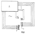
- Figure 1 shows the block diagram of the operation of the scanning driver circuit 1.
- a time T1 it turns on a light source 3 (I) whose light is directed towards several photodetectors 2 (ABC..GH). Each of them receives the light energy and testifies it to the pilot circuit by sending back to it a current which rises above a determined excitation threshold. The result of this scan is processed by the pilot circuit.
- time T2 it is the next light source II in the sequence which is put into operation, and so on, until the lighting of the last light source (XVI) which marks the end of a cycle all the keyboard.
- XVI last light source
- One of the preferred solutions in the present embodiment consists in taking as the start of each scanning cycle of a light source the moment when the slowest of the photodetectors is capable of receiving new information reliably. This instant is determined by measuring the residual voltages at the terminals of the photodetectors with reference to a de-excitation threshold.
- a pre-signal 29 (Fig. 2) can be used to carry out this measurement and check the correct functioning of the keyboard by analyzing the reactions of the photodetectors. This light signal is sent to the photodetectors until all of them have crossed a determined excitation threshold. Once this threshold is reached, it is ensured that all the photodetectors return to the de-excitation threshold.
- an error message can be sent to the system to which the keyboard is connected.
- FIG. 2 An exemplary embodiment of the verification pre-signal is shown in FIG. 2. It relates to an optical keyboard comprising a rectangular housing 21 traversed by pairs of fibers 23, 22 one of which brings light and the other reports the signal. These two fibers meet towards a switch 25 controlled by a key.
- This pre-signal is achieved here by providing specific fibers. Unlike ordinary fibers, the specific fibers 28 which allow the light source to emit a signal on the receiving transducers are not cut. When the light source 29 sends a pre-signal, all the receivers are therefore directly illuminated whatever the state of the keys. So we can also measure the reaction times of the different receivers, determine which is the first to activate and which is the last to deactivate, as well as accentuate the sensitivity of the receivers before sending the detection signal to light sources 23.
- FIG. 3 Another embodiment (Fig. 3) relates to a keyboard with fixed mirrors. It consists of a hollow housing 31 surrounded by several edges in which covers 37 are included. In the example shown in FIG. 3, the optical unit is rectangular. Two of its adjacent edges comprise light means 33 and detection elements 32. To increase the power and the sensitivity of the assembly, it is possible to reduce the distances and to install emission or detection components on the third, and even the fourth edge of the housing, which amounts in fact to implanting several matrices on the same optical unit. Better use of the energy emitted can also result from the installation of two rows of mirrors (not shown forming a given angle facing each light source.
- the reflectors are located inside the support at a point close to the intersections of the emission rows and the columns of detectors.
- Light 36 is returned from columns 33 to rows 32 by means of small reflectors 35 placed so that they do not interfere with each other.
- a key 34 When a key 34 is pressed, it causes the shutter of one of these reflectors or on the contrary releases it from its shutter.
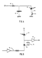
- FIG. 4 gives an exemplary embodiment making it possible to very substantially increase the power of the emission of a light source 43 thanks to the presence of a reservoir capacitor 42 serving as a source of great instantaneous power.
- a current limiting resistor 41 is provided in the circuit to allow recharging of the reservoir capacitor 42 before the next pulse.
- a switch of the transitor type 44 triggers the discharge of the reservoir capacitor 42 through the light source 43, which here is an LED diode, when a control pulse is sent to its base.
- FIG. 5 provides an exemplary embodiment making it possible to increase the sensitivity of the photodetectors: by means of a reset circuit 54, the parasitic input capacitance 51 is discharged at a reference voltage, such as 0 volts through a switching device such as a CMOS diode or relay 53 under the control of a reset signal. Then the reset circuit 54 returns to a working voltage, such as 5 volts, and the diode 55 is blocked. In the event that the photodiode 52 does not receive light, the capacitor 51 remains at 0 volts. When it receives a light pulse, the capacitor 51 charges at 5 volts and remains charged until the next reset signal. The output of the MOS amplifier 53 restores the output of the voltage state on the capacitor 51.
- a reference voltage such as 0 volts
- a switching device such as a CMOS diode or relay 53
- the reset circuit 54 returns to a working voltage, such as 5 volts, and the diode 55 is blocked.
- the capacitor 51 remains
Landscapes
- Electronic Switches (AREA)
- Push-Button Switches (AREA)
Claims (9)
Priority Applications (1)
| Application Number | Priority Date | Filing Date | Title |
|---|---|---|---|
| AT87902559T ATE70676T1 (de) | 1986-04-25 | 1987-04-27 | Optisches tastenfeld mit erhoehter empfindlichkeit. |
Applications Claiming Priority (2)
| Application Number | Priority Date | Filing Date | Title |
|---|---|---|---|
| FR8606067A FR2597988A1 (fr) | 1986-04-25 | 1986-04-25 | Amelioration des claviers optiques a balayage matriciel |
| FR8606067 | 1986-04-25 |
Publications (2)
| Publication Number | Publication Date |
|---|---|
| EP0265472A1 EP0265472A1 (de) | 1988-05-04 |
| EP0265472B1 true EP0265472B1 (de) | 1991-12-18 |
Family
ID=9334652
Family Applications (1)
| Application Number | Title | Priority Date | Filing Date |
|---|---|---|---|
| EP87902559A Expired - Lifetime EP0265472B1 (de) | 1986-04-25 | 1987-04-27 | Optisches tastenfeld mit erhöhter empfindlichkeit |
Country Status (7)
| Country | Link |
|---|---|
| US (1) | US4884073A (de) |
| EP (1) | EP0265472B1 (de) |
| JP (1) | JPS63503188A (de) |
| AT (1) | ATE70676T1 (de) |
| DE (1) | DE3775337D1 (de) |
| FR (1) | FR2597988A1 (de) |
| WO (1) | WO1987006782A1 (de) |
Families Citing this family (41)
| Publication number | Priority date | Publication date | Assignee | Title |
|---|---|---|---|---|
| GB9119092D0 (en) * | 1991-09-06 | 1991-10-23 | Sarnoff David Res Center | Optomechanical keyboard |
| AU6667994A (en) | 1993-04-28 | 1994-11-21 | R. Douglas Mcpheters | Holographic operator interface |
| US6741189B1 (en) * | 1999-10-06 | 2004-05-25 | Microsoft Corporation | Keypad having optical waveguides |
| DE10031794C2 (de) * | 2000-07-04 | 2003-10-02 | Gallitzendoerfer Rainer | Klaviatur für elektronische Musikinstrumente |
| US7042371B2 (en) * | 2004-02-24 | 2006-05-09 | Nokia Corporation | Optical keyboard with geodesic optical elements |
| IL176673A0 (en) * | 2006-07-03 | 2007-07-04 | Fermon Israel | A variably displayable mobile device keyboard |
| US7924175B2 (en) * | 2007-03-26 | 2011-04-12 | Motorola Mobility, Inc. | Optical keypad for electronic device |
| US9542016B2 (en) | 2012-09-13 | 2017-01-10 | Apple Inc. | Optical sensing mechanisms for input devices |
| US9753436B2 (en) | 2013-06-11 | 2017-09-05 | Apple Inc. | Rotary input mechanism for an electronic device |
| KR20220116337A (ko) | 2013-08-09 | 2022-08-22 | 애플 인크. | 전자 디바이스용 촉각 스위치 |
| US10048802B2 (en) | 2014-02-12 | 2018-08-14 | Apple Inc. | Rejection of false turns of rotary inputs for electronic devices |
| US10190891B1 (en) | 2014-07-16 | 2019-01-29 | Apple Inc. | Optical encoder for detecting rotational and axial movement |
| US9797752B1 (en) | 2014-07-16 | 2017-10-24 | Apple Inc. | Optical encoder with axially aligned sensor |
| US10066970B2 (en) | 2014-08-27 | 2018-09-04 | Apple Inc. | Dynamic range control for optical encoders |
| US9797753B1 (en) | 2014-08-27 | 2017-10-24 | Apple Inc. | Spatial phase estimation for optical encoders |
| KR102130259B1 (ko) | 2014-09-02 | 2020-07-03 | 애플 인크. | 웨어러블 전자 디바이스 |
| JP6515185B2 (ja) | 2015-03-05 | 2019-05-15 | アップル インコーポレイテッドApple Inc. | 方向依存光学特性を有する光学エンコーダを有する時計、手首装着型電子デバイス及びウェラブル電子デバイス |
| EP3251139B1 (de) | 2015-03-08 | 2021-04-28 | Apple Inc. | Komprimierbare dichtung für drehbare und verschiebbare eingabemechanismen |
| US9952682B2 (en) | 2015-04-15 | 2018-04-24 | Apple Inc. | Depressible keys with decoupled electrical and mechanical functionality |
| US10018966B2 (en) | 2015-04-24 | 2018-07-10 | Apple Inc. | Cover member for an input mechanism of an electronic device |
| US9891651B2 (en) | 2016-02-27 | 2018-02-13 | Apple Inc. | Rotatable input mechanism having adjustable output |
| US10551798B1 (en) | 2016-05-17 | 2020-02-04 | Apple Inc. | Rotatable crown for an electronic device |
| US10061399B2 (en) | 2016-07-15 | 2018-08-28 | Apple Inc. | Capacitive gap sensor ring for an input device |
| US10019097B2 (en) | 2016-07-25 | 2018-07-10 | Apple Inc. | Force-detecting input structure |
| US10664074B2 (en) | 2017-06-19 | 2020-05-26 | Apple Inc. | Contact-sensitive crown for an electronic watch |
| US10962935B1 (en) | 2017-07-18 | 2021-03-30 | Apple Inc. | Tri-axis force sensor |
| US11360440B2 (en) | 2018-06-25 | 2022-06-14 | Apple Inc. | Crown for an electronic watch |
| US11561515B2 (en) | 2018-08-02 | 2023-01-24 | Apple Inc. | Crown for an electronic watch |
| CN211293787U (zh) | 2018-08-24 | 2020-08-18 | 苹果公司 | 电子表 |
| US12259690B2 (en) | 2018-08-24 | 2025-03-25 | Apple Inc. | Watch crown having a conductive surface |
| US11181863B2 (en) | 2018-08-24 | 2021-11-23 | Apple Inc. | Conductive cap for watch crown |
| CN209625187U (zh) | 2018-08-30 | 2019-11-12 | 苹果公司 | 电子手表和电子设备 |
| US11194298B2 (en) | 2018-08-30 | 2021-12-07 | Apple Inc. | Crown assembly for an electronic watch |
| US11194299B1 (en) | 2019-02-12 | 2021-12-07 | Apple Inc. | Variable frictional feedback device for a digital crown of an electronic watch |
| CN111312547B (zh) * | 2019-06-18 | 2023-08-04 | 光宝电子(广州)有限公司 | 按键模块、应用其的键盘及电子装置 |
| US11550268B2 (en) | 2020-06-02 | 2023-01-10 | Apple Inc. | Switch module for electronic crown assembly |
| US11269376B2 (en) | 2020-06-11 | 2022-03-08 | Apple Inc. | Electronic device |
| US12092996B2 (en) | 2021-07-16 | 2024-09-17 | Apple Inc. | Laser-based rotation sensor for a crown of an electronic watch |
| US12189347B2 (en) | 2022-06-14 | 2025-01-07 | Apple Inc. | Rotation sensor for a crown of an electronic watch |
| US12596334B2 (en) | 2023-02-07 | 2026-04-07 | Apple Inc. | Crown for an electronic watch |
| US12669784B2 (en) | 2023-03-24 | 2026-06-30 | Apple Inc. | Crown sensing system for an electronic watch |
Family Cites Families (6)
| Publication number | Priority date | Publication date | Assignee | Title |
|---|---|---|---|---|
| EP0004520A1 (de) * | 1978-03-24 | 1979-10-03 | International Business Machines Corporation | Tastatur mit einer aus Lichtteilern aufgebauten Matrix |
| US4319144A (en) * | 1980-05-22 | 1982-03-09 | Bell Telephone Laboratories, Incorporated | Single polarity circuit |
| US4379968A (en) * | 1980-12-24 | 1983-04-12 | Burroughs Corp. | Photo-optical keyboard having light attenuating means |
| US4652741A (en) * | 1984-11-08 | 1987-03-24 | Spacelabs Inc. | Radiant beam coordinate detector |
| US4672195A (en) * | 1984-11-08 | 1987-06-09 | Spacelabs, Inc. | Radiant beam coordinate detector system |
| AU4907185A (en) * | 1984-11-08 | 1986-05-15 | Spacelabs, Inc. | Radiant beam co-ordinate detector system |
-
1986
- 1986-04-25 FR FR8606067A patent/FR2597988A1/fr active Pending
-
1987
- 1987-04-27 DE DE8787902559T patent/DE3775337D1/de not_active Expired - Lifetime
- 1987-04-27 WO PCT/FR1987/000141 patent/WO1987006782A1/fr not_active Ceased
- 1987-04-27 AT AT87902559T patent/ATE70676T1/de active
- 1987-04-27 EP EP87902559A patent/EP0265472B1/de not_active Expired - Lifetime
- 1987-04-27 JP JP62502671A patent/JPS63503188A/ja active Pending
- 1987-12-23 US US07/143,162 patent/US4884073A/en not_active Expired - Fee Related
Non-Patent Citations (1)
| Title |
|---|
| Electronique et applications Industrielles, n0 255, June 1978 (Paris, FR), P. Vernel et al.: "Clavier à voter à faisceaux infrarouges", pages 57-59 * |
Also Published As
| Publication number | Publication date |
|---|---|
| WO1987006782A1 (fr) | 1987-11-05 |
| FR2597988A1 (fr) | 1987-10-30 |
| DE3775337D1 (de) | 1992-01-30 |
| US4884073A (en) | 1989-11-28 |
| ATE70676T1 (de) | 1992-01-15 |
| JPS63503188A (ja) | 1988-11-17 |
| EP0265472A1 (de) | 1988-05-04 |
Similar Documents
| Publication | Publication Date | Title |
|---|---|---|
| WO1987006782A1 (fr) | Clavier optique a sensibilite accrue | |
| US11294037B2 (en) | Detecting light using a plurality of avalanche photodiode elements | |
| US6794725B2 (en) | Amorphous silicon sensor with micro-spring interconnects for achieving high uniformity in integrated light-emitting sources | |
| EP0034957B1 (de) | Vorrichtung zur automatischen Regulierung der Ausgangsleistung eines Sendermoduls für ein Übertragungssystem mit optischen Fasern | |
| EP3900322A1 (de) | Grossflächiger einzelphotonendetektor mit zeitausblendungsfähigkeit | |
| JPH09219552A (ja) | 一体化レーザ・ベース光源 | |
| JPH09214066A (ja) | 一体化レーザ・ベース光源 | |
| US7218388B1 (en) | VCSEL fault location apparatus and method | |
| EP0586285B1 (de) | Optischer Sender-Empfänger für optische Datenübertragung und Schalteinrichtung | |
| KR102518342B1 (ko) | 광섬유들에 대한 측정 디바이스 및 방법 | |
| FR2707394A1 (fr) | Elément et détecteur photosensibles pour la détection d'éclats lumineux. | |
| FR2753785A1 (fr) | Autodirecteur d'un corps volant | |
| EP0014634A1 (de) | Aktive Kopplungsanordnung zwischen einer optischen Bus-Leitung und einem der Teilnehmern und Bus-Leitung, die solche Kopplungsanordnungen enthält | |
| EP0357468B1 (de) | Photoempfindliche Matrix mit zwei Dioden gleicher Polarität und einer Kapazität pro photoempfindlichem Punkt | |
| FR2753796A1 (fr) | Detecteur photosensible et mosaique de detecteurs photosensibles pour la detection d'eclats lumineux et applications | |
| EP0509920B1 (de) | Positionsmeldevorrichtung eines beweglichen Gliedes | |
| US20040021144A1 (en) | Carrier for opto-electronic elements, an optical transmitter and an optical receiver | |
| JP2002280655A (ja) | 光出力装置および光出力装置用レンズ素子 | |
| JPH10215020A (ja) | 一体化レーザ・ベース光源 | |
| FR2459591A1 (fr) | Procede et dispositif de telecopie a sauts de blancs | |
| JPH06303206A (ja) | 耐放射線型光ファイバ信号伝送路並びに同信号伝送路を利用した光通信システム及び放射線計測システム | |
| FR3149097A1 (fr) | Système télémétrie d’un véhicule automobile comportant un module de réception d’un faisceau lumineux | |
| JPH0346588A (ja) | レーザ受信器 | |
| EP0439382B1 (de) | Verfahren und Vorrichtung zur Begrenzung eines Kathodenröhrestroms | |
| WO2026017660A1 (fr) | Système lumineux d'un véhicule automobile comportant un dispositif d'alimentation électrique auxiliaire |
Legal Events
| Date | Code | Title | Description |
|---|---|---|---|
| PUAI | Public reference made under article 153(3) epc to a published international application that has entered the european phase |
Free format text: ORIGINAL CODE: 0009012 |
|
| AK | Designated contracting states |
Kind code of ref document: A1 Designated state(s): AT BE CH DE FR GB IT LI LU NL SE |
|
| 17P | Request for examination filed |
Effective date: 19880419 |
|
| 17Q | First examination report despatched |
Effective date: 19900328 |
|
| GRAA | (expected) grant |
Free format text: ORIGINAL CODE: 0009210 |
|
| AK | Designated contracting states |
Kind code of ref document: B1 Designated state(s): AT BE CH DE FR GB IT LI LU NL SE |
|
| PG25 | Lapsed in a contracting state [announced via postgrant information from national office to epo] |
Ref country code: IT Free format text: LAPSE BECAUSE OF FAILURE TO SUBMIT A TRANSLATION OF THE DESCRIPTION OR TO PAY THE FEE WITHIN THE PRE;WARNING: LAPSES OF ITALIAN PATENTS WITH EFFECTIVE DATE BEFORE 2007 MAY HAVE OCCURRED AT ANY TIME BEFORE 2007. THE CORRECT EFFECTIVE DATE MAY BE DIFFERENT FROM THE ONE RECORDED.SCRIBED TIME-LIMIT Effective date: 19911218 Ref country code: NL Effective date: 19911218 Ref country code: SE Effective date: 19911218 Ref country code: AT Effective date: 19911218 |
|
| REF | Corresponds to: |
Ref document number: 70676 Country of ref document: AT Date of ref document: 19920115 Kind code of ref document: T |
|
| REF | Corresponds to: |
Ref document number: 3775337 Country of ref document: DE Date of ref document: 19920130 |
|
| GBT | Gb: translation of ep patent filed (gb section 77(6)(a)/1977) | ||
| PG25 | Lapsed in a contracting state [announced via postgrant information from national office to epo] |
Ref country code: BE Effective date: 19920430 Ref country code: LI Effective date: 19920430 Ref country code: CH Effective date: 19920430 Ref country code: LU Free format text: LAPSE BECAUSE OF NON-PAYMENT OF DUE FEES Effective date: 19920430 |
|
| NLV1 | Nl: lapsed or annulled due to failure to fulfill the requirements of art. 29p and 29m of the patents act | ||
| PLBE | No opposition filed within time limit |
Free format text: ORIGINAL CODE: 0009261 |
|
| STAA | Information on the status of an ep patent application or granted ep patent |
Free format text: STATUS: NO OPPOSITION FILED WITHIN TIME LIMIT |
|
| BERE | Be: lapsed |
Owner name: SOULOUMIAC ALAIN Effective date: 19920430 |
|
| 26N | No opposition filed | ||
| REG | Reference to a national code |
Ref country code: CH Ref legal event code: AUV Free format text: LE BREVET CI-DESSUS EST TOMBE EN DECHEANCE FAUTE DE PAIEMENT, DE LA 6E ANNUITE. Ref country code: CH Ref legal event code: PL |
|
| PGFP | Annual fee paid to national office [announced via postgrant information from national office to epo] |
Ref country code: DE Payment date: 19930426 Year of fee payment: 7 Ref country code: GB Payment date: 19930426 Year of fee payment: 7 |
|
| PGFP | Annual fee paid to national office [announced via postgrant information from national office to epo] |
Ref country code: FR Payment date: 19930430 Year of fee payment: 7 |
|
| PG25 | Lapsed in a contracting state [announced via postgrant information from national office to epo] |
Ref country code: GB Effective date: 19940427 |
|
| GBPC | Gb: european patent ceased through non-payment of renewal fee |
Effective date: 19940427 |
|
| PG25 | Lapsed in a contracting state [announced via postgrant information from national office to epo] |
Ref country code: FR Effective date: 19941229 |
|
| PG25 | Lapsed in a contracting state [announced via postgrant information from national office to epo] |
Ref country code: DE Effective date: 19950103 |
|
| REG | Reference to a national code |
Ref country code: FR Ref legal event code: ST |