EP0262284B1 - Verbindungsgerät für integrierte Schaltung - Google Patents
Verbindungsgerät für integrierte Schaltung Download PDFInfo
- Publication number
- EP0262284B1 EP0262284B1 EP87101550A EP87101550A EP0262284B1 EP 0262284 B1 EP0262284 B1 EP 0262284B1 EP 87101550 A EP87101550 A EP 87101550A EP 87101550 A EP87101550 A EP 87101550A EP 0262284 B1 EP0262284 B1 EP 0262284B1
- Authority
- EP
- European Patent Office
- Prior art keywords
- circuit board
- substrate
- main face
- clamp member
- face
- Prior art date
- Legal status (The legal status is an assumption and is not a legal conclusion. Google has not performed a legal analysis and makes no representation as to the accuracy of the status listed.)
- Expired - Lifetime
Links
Images
Classifications
-
- H—ELECTRICITY
- H05—ELECTRIC TECHNIQUES NOT OTHERWISE PROVIDED FOR
- H05K—PRINTED CIRCUITS; CASINGS OR CONSTRUCTIONAL DETAILS OF ELECTRIC APPARATUS; MANUFACTURE OF ASSEMBLAGES OF ELECTRICAL COMPONENTS
- H05K7/00—Constructional details common to different types of electric apparatus
- H05K7/02—Arrangements of circuit components or wiring on supporting structure
- H05K7/10—Plug-in assemblages of components, e.g. IC sockets
- H05K7/1053—Plug-in assemblages of components, e.g. IC sockets having interior leads
- H05K7/1061—Plug-in assemblages of components, e.g. IC sockets having interior leads co-operating by abutting
-
- H—ELECTRICITY
- H01—ELECTRIC ELEMENTS
- H01L—SEMICONDUCTOR DEVICES NOT COVERED BY CLASS H10
- H01L23/00—Details of semiconductor or other solid state devices
- H01L23/12—Mountings, e.g. non-detachable insulating substrates
- H01L23/13—Mountings, e.g. non-detachable insulating substrates characterised by the shape
-
- H—ELECTRICITY
- H05—ELECTRIC TECHNIQUES NOT OTHERWISE PROVIDED FOR
- H05K—PRINTED CIRCUITS; CASINGS OR CONSTRUCTIONAL DETAILS OF ELECTRIC APPARATUS; MANUFACTURE OF ASSEMBLAGES OF ELECTRICAL COMPONENTS
- H05K1/00—Printed circuits
- H05K1/02—Details
- H05K1/0201—Thermal arrangements, e.g. for cooling, heating or preventing overheating
- H05K1/0203—Cooling of mounted components
- H05K1/0204—Cooling of mounted components using means for thermal conduction connection in the thickness direction of the substrate
-
- H—ELECTRICITY
- H01—ELECTRIC ELEMENTS
- H01L—SEMICONDUCTOR DEVICES NOT COVERED BY CLASS H10
- H01L2224/00—Indexing scheme for arrangements for connecting or disconnecting semiconductor or solid-state bodies and methods related thereto as covered by H01L24/00
- H01L2224/01—Means for bonding being attached to, or being formed on, the surface to be connected, e.g. chip-to-package, die-attach, "first-level" interconnects; Manufacturing methods related thereto
- H01L2224/42—Wire connectors; Manufacturing methods related thereto
- H01L2224/47—Structure, shape, material or disposition of the wire connectors after the connecting process
- H01L2224/48—Structure, shape, material or disposition of the wire connectors after the connecting process of an individual wire connector
- H01L2224/481—Disposition
- H01L2224/48151—Connecting between a semiconductor or solid-state body and an item not being a semiconductor or solid-state body, e.g. chip-to-substrate, chip-to-passive
- H01L2224/48221—Connecting between a semiconductor or solid-state body and an item not being a semiconductor or solid-state body, e.g. chip-to-substrate, chip-to-passive the body and the item being stacked
- H01L2224/48225—Connecting between a semiconductor or solid-state body and an item not being a semiconductor or solid-state body, e.g. chip-to-substrate, chip-to-passive the body and the item being stacked the item being non-metallic, e.g. insulating substrate with or without metallisation
- H01L2224/48227—Connecting between a semiconductor or solid-state body and an item not being a semiconductor or solid-state body, e.g. chip-to-substrate, chip-to-passive the body and the item being stacked the item being non-metallic, e.g. insulating substrate with or without metallisation connecting the wire to a bond pad of the item
-
- H—ELECTRICITY
- H05—ELECTRIC TECHNIQUES NOT OTHERWISE PROVIDED FOR
- H05K—PRINTED CIRCUITS; CASINGS OR CONSTRUCTIONAL DETAILS OF ELECTRIC APPARATUS; MANUFACTURE OF ASSEMBLAGES OF ELECTRICAL COMPONENTS
- H05K1/00—Printed circuits
- H05K1/18—Printed circuits structurally associated with non-printed electric components
- H05K1/182—Printed circuits structurally associated with non-printed electric components associated with components mounted in the printed circuit board, e.g. insert mounted components [IMC]
-
- H—ELECTRICITY
- H05—ELECTRIC TECHNIQUES NOT OTHERWISE PROVIDED FOR
- H05K—PRINTED CIRCUITS; CASINGS OR CONSTRUCTIONAL DETAILS OF ELECTRIC APPARATUS; MANUFACTURE OF ASSEMBLAGES OF ELECTRICAL COMPONENTS
- H05K2201/00—Indexing scheme relating to printed circuits covered by H05K1/00
- H05K2201/10—Details of components or other objects attached to or integrated in a printed circuit board
- H05K2201/10227—Other objects, e.g. metallic pieces
- H05K2201/10409—Screws
-
- H—ELECTRICITY
- H05—ELECTRIC TECHNIQUES NOT OTHERWISE PROVIDED FOR
- H05K—PRINTED CIRCUITS; CASINGS OR CONSTRUCTIONAL DETAILS OF ELECTRIC APPARATUS; MANUFACTURE OF ASSEMBLAGES OF ELECTRICAL COMPONENTS
- H05K2201/00—Indexing scheme relating to printed circuits covered by H05K1/00
- H05K2201/10—Details of components or other objects attached to or integrated in a printed circuit board
- H05K2201/10227—Other objects, e.g. metallic pieces
- H05K2201/10416—Metallic blocks or heatsinks completely inserted in a PCB
-
- H—ELECTRICITY
- H05—ELECTRIC TECHNIQUES NOT OTHERWISE PROVIDED FOR
- H05K—PRINTED CIRCUITS; CASINGS OR CONSTRUCTIONAL DETAILS OF ELECTRIC APPARATUS; MANUFACTURE OF ASSEMBLAGES OF ELECTRICAL COMPONENTS
- H05K2201/00—Indexing scheme relating to printed circuits covered by H05K1/00
- H05K2201/10—Details of components or other objects attached to or integrated in a printed circuit board
- H05K2201/10613—Details of electrical connections of non-printed components, e.g. special leads
- H05K2201/10621—Components characterised by their electrical contacts
- H05K2201/10727—Leadless chip carrier [LCC], e.g. chip-modules for cards
-
- H—ELECTRICITY
- H05—ELECTRIC TECHNIQUES NOT OTHERWISE PROVIDED FOR
- H05K—PRINTED CIRCUITS; CASINGS OR CONSTRUCTIONAL DETAILS OF ELECTRIC APPARATUS; MANUFACTURE OF ASSEMBLAGES OF ELECTRICAL COMPONENTS
- H05K3/00—Apparatus or processes for manufacturing printed circuits
- H05K3/30—Assembling printed circuits with electric components, e.g. with resistor
- H05K3/32—Assembling printed circuits with electric components, e.g. with resistor electrically connecting electric components or wires to printed circuits
- H05K3/325—Assembling printed circuits with electric components, e.g. with resistor electrically connecting electric components or wires to printed circuits by abutting or pinching, i.e. without alloying process; mechanical auxiliary parts therefor
Definitions
- This invention relates to connection apparatus for integrated circuits.
- U.S. Patent No. 4,255,003 discloses a device for connecting a monolithic integrated circuit to a circuit board.
- the monolithic integrated circuit is mounted on a rectangular ceramic substrate that has connection pads distributed about the periphery of one main face of the substrate.
- the circuit board has corresponding connection pads exposed at one main face of the board about the periphery of a rectangular "footprint" region corresponding in shape and size to the main face of the ceramic substrate.
- the circuit board is formed with holes outside the footprint region.
- a clamping member has four rigid side portions that are connected together and form a rectangular frame. The side portions are formed with an endless groove at the underside of the frame.
- a frame-like body of elastomeric material projects downwardly from the underside of the clamping member and has a locating ridge that fits in the groove of the clamping member.
- Strips of conductive material are bonded to the underside of the body of elastomeric material.
- the elastomeric material is silicone rubber.
- the clamping member has an ear that extends downwardly somewhat beyond the underside of the frame, and each ear is formed with a hole.
- the circuit board is formed with corresponding holes. Through use of screws extending downwardly through the holes in the ears and the corresponding holes in the circuit board, and nuts engaging the lower ends of the screws, the clamping member may be attached to the circuit board.
- the elastomeric material When the clamping member is so attached, the elastomeric material is compressed and the strips of conductive material provide electrical connection between the connection pads of the substrate and the corresponding connection pads of the circuit board. The compression of the elastomeric material provides contact force between the strips of conductive material and the contact pads.
- a practical implementation of the conventional connection device disclosed in Patent No. 4,255,003 is designed for use with a substrate that is about 0.64 mm thick.
- the underside of the frame is stepped, in that the lower surface portion that is inward of the groove is at a height of 1.45 mm above the bottom of the ears and the lower surface portion that is outward of the groove is at a height of 0.81 mm above the bottom of the ears.
- the body of elastomeric material has two lobes, for engaging the substrate and the circuit board respectively, and each extends 1.02 mm downwards from the relevant surface portion of the frame.
- each lobe When the clamping member is attached to the circuit board and the screws are tightened, each lobe is compressed to a thickness of 0.81 mm, so that the percentage compression of each lobe is about 20%.
- manufacturing tolerances result in the percentage compression of the lobes possibly being different from 20%. Nevertheless, the tolerances are sufficiently small, e.g. ⁇ 0.05 mm on each component, that for all values of the percentage compression permitted by the manufacturing tolerances, adequate contact force is provided between the conductive strips and the pads of the substrate.
- the main mechanism for dissipation of heat from the integrated circuit is by conduction downwards through the ceramic substrate into the circuit board. Heat is removed from the bottom face of the circuit board by convection and/or conduction.
- Circuit board material e.g. epoxy glass
- the practical implementation of the conventional connection device is designed for use with circuit boards no thicker than about 0.64 mm, i.e. single layer circuit boards. It is, however, desirable to be able to use multilayer circuit boards that are about 1.57 mm thick.
- the high thermal resistance of such a circuit board places a relatively low limit on the amount of power that can be dissipated as heat without causing the temperature of the circuit board to increase excessively and consequently causing damage to the circuit board.
- connection apparatus as defined in claim 1.
- An intergrated circuit is mounted on the front face of a substrate of dielectric material and the substrate is fitted in an aperture that extends through a circuit board.
- the substrate has contact elements distributed about the periphery of its front face, and the circuit board has corresponding contact elements on its front face distributed about the periphery of the aperture.
- a first clamping member is positioned at the back face of the circuit board so as to extend over the aperture in the circuit board.
- the first clamping member is made of thermally-conductive material and is in thermally-conductive contact with the back face of the substrate.
- a second clamping member is positioned at the front face of the circuit board and extends at least partially over the peripheral area of the front face of the substrate.
- a resilient member is effective between the second clamping member and both the substrate and the circuit board. Fastening elements are used to draw the clamping members together and thereby press the resilient member into firm contact with the substrate and the circuit board.
- the resilient member has portions of conductive material that connect the contact elements of the substrate to the corresponding contact elements of the circuit board.
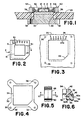
- a hybrid integrated circuit 2 comprises a monolithic integrated circuit chip that is mounted on a substrate 6 of ceramic material.
- the contact pads of the chip are connected to conductor runs 8 of the substrate by bondwires (not shown).
- a lid 10 is fitted over the chip and is attached to the substrate, leaving the peripheral region of the substrate exposed.
- the conductor runs 8 extend under the rim of the lid and terminate in contact pads 8a that are exposed in the peripheral region of the substrate.
- the substrate is generally square in shape, but has one corner cut off at 45 degrees.
- a circuit board 20 is formed with an aperture 22 that extends right through the circuit board and is of the same shape as the substrate.
- the aperture is square, except that it has one corner cut off at 45 degrees.
- the substrate is placed in the aperture of the circuit board, and the shaping of the substrate 6 and the aperture 22 ensures that the substrate can be inserted into the aperture in only one position.
- the circuit board includes conductor runs 24 that terminate about the periphery of the aperture in respective connection pads 24a.
- the connection pads 24a are distributed about the aperture in a pattern that corresponds to the pattern of terminal areas 8a about the peripheral region of the substrate.
- the circuit board is formed with holes 26, one adjacent each corner of the aperture 22. The aperture 22 and the holes 26 are precisely positioned relative to the connection pads 24a.
- a metal heat sink member 30 is in the form of a generally rectangular plate having ears 32 at its four corners and a pedestal 34 at its upper surface.
- the cross-sectional shape of the pedestal is substantially the same as the shape of the substrate and the aperture, i.e. square with one corner cut off at 45 degrees.
- the ears 32 are formed with internally threaded holes 36 that are at the same positions relative to the pedestal as the holes 26 in the circuit board are relative to the aperture 22. Thus, when the pedestal 34 is inserted upwardly into the aperture 22, the holes 36 of the heat sink member are aligned with the holes 26 of the circuit board.
- a retaining frame 40 has four sides 42 and is generally square in configuration. At the underside of the frame, the four sides are formed with an endless recess 46.
- a frame-like body 48 of elastomeric material has discrete strips 50 of metal bonded to its lower face and includes a ridge 52 that extends upwardly and fits in the recess 46 of the retaining frame.
- the retaining frame includes an ear 54 at each corner, similar to the head sink member 30, and each ear is formed with a hole 56. The positioning of the holes 56 relative to each other is the same as that of the holes 26 in the circuit board.
- the ears 54 extend downwardly beyond the sides 42 of the frame and have abutment surfaces 58.
- the frame 40 is identical to the frame that is used in the practical implementation of the device described in U.S. Patent No. 4,255,003.
- the inner lower surface portion 60a is at a height of 1.45 mm relative to the abutment surfaces 58 of the ears 54 (which coincide with the top face of the circuit board), whereas the outer lower surface portion 60b is at a height of 0.81 mm.
- the body of elastomeric material is similar to that which is used in the practical implementation of the device described in U.S. Patent No. 4,255,003, and has inner and outer lobes 62a and 62b that define a groove 66 therebetween.
- the lobe 62b extends 1.02 mm below the surface 60b
- the lobe 62a extends 1.65 mm below the surface 60a.
- the metal strips 50 may be of substantially the same width (0.64 mm) and at substantially the same spacing (0.64 mm) as the connection pads 8a and 24a. However, it is preferred that the strips be narrower than the pads 8a and 24a, and at a smaller spacing (e.g. 0.51 mm wide and with 0.51 mm spaces), in order to enlarge the tolerance in positioning of the body 48 relative to the circuit board.
- the body 48 may be made using the techniques disclosed in co-pending Application EP-A-87 101 551 Screws 64 are fitted through the holes 56 of the retaining frame and the holes 26 of the circuit board and engage the holes 36 of the heat sink member and are used to draw the retaining frame and the heat sink member together.
- the body of elastomeric material is compressed between the sides of the frame and both the circuit board and the substrate. Engagement of the abutment surfaces 58 of the ears 54 of the frame with the upper surface of the circuit board limits the extent to which the elastomeric material is compressed.
- the strips 50 of conductive material contact the contact pads 8a of the substrate and the contact pads 24a of the circuit board.
- Compression of the elastomeric material provides contact force for the pressure contact between the conductive strips and the contact pads, and also maintains the back face of the substrate in contact with the pedestal of the heat sink member. Therefore, electrical connection is provided between each substrate pad 8a and the corresponding circuit board pad 24a, and a good thermally-conductive contact is provided between the substrate and the heat sink member.
- the amount of heat that can be removed from the chip 4 is essentially independent of the thickness and nature of the circuit board 20.
- the thickness of the substrate 6, the thickness of the circuit board 20 and the height of the pedestal 34 are selected so that the top face of the substrate 6 is nominally flush with the top face of the circuit board 20, and therefore when the screws 64 are tightened, the inner lobe is compressed to a thickness of 1.45 mm.
- This degree of compression provides adequate contact force between the metal strips 50 and the contact pads 8a.
- the actual position of the top face of the substrate relative to the top face of the circuit board depends on manufacturing tolerances, which are such that the range of probable values for the contact force between the metal strips 50 and the contact pads 6a are acceptable.
Landscapes
- Engineering & Computer Science (AREA)
- Microelectronics & Electronic Packaging (AREA)
- Physics & Mathematics (AREA)
- Condensed Matter Physics & Semiconductors (AREA)
- General Physics & Mathematics (AREA)
- Computer Hardware Design (AREA)
- Power Engineering (AREA)
- Combinations Of Printed Boards (AREA)
- Cooling Or The Like Of Electrical Apparatus (AREA)
- Cooling Or The Like Of Semiconductors Or Solid State Devices (AREA)
Claims (6)
- Verbindungsgerät mit der Kombination folgender Komponenten:
einer Schaltungsplatte (20) mit einer ersten und einer zweiten gegenüberliegenden Hauptfläche und mit einer Öffnung (22) aus dielektrischem Material und Bahnen (24) aus leitendem Material, die auf dem dielektrischen Material elektrisch isoliert voneinander liegen und in Anschlußflecken (24a) enden, welche an der ersten Hauptfläche der Schaltungsplatte (20) frei liegen und am Umfang der Öffnung (22) der Schaltungsplatte (20) verteilt sind,
einem Substrat (6) aus dielektrischem Material mit einer ersten und einer zweiten gegenüberliegenden Hauptfläche, das in die Öffnung (22) der Schaltungsplatte (20) eingepaßt ist,
Leiterbahnen (8) auf der ersten Hauptfläche des Substrates (6), welche in zugehörigen Anschlußflecken (8a) enden, die um einen Umfangsbereich der ersten Hauptfläche verteilt sind,
einem auf der ersten Hauptfläche des Substrats (6) montierten Chip (10) einer integrierten Schaltung,
einem mit der zweiten Hauptfläche der Schaltungsplatte (20) in Eingriff stehenden ersten Klemmelement (30),
einem zweiten Klemmelement (40),
einem federnden Element (48) aus dielektrischem Material mit Teilen (50) aus leitendem Material, die isoliert voneinander auf dem dielektrischen Material angeordnet sind und an einer Fläche des federnden Elementes (48) frei liegen, wobei das federnde Element (48) mit dem zweiten Klemmelement (40) in Eingriff steht und mit der genannten Fläche sowohl dem Substrat (6) und der Schaltungsplatte (20) zugekehrt ist, und
einer Befestigungseinrichtung (64), welche mit den Klemmelementen (30, 40) in Eingriff steht und das erste Klemmelement (30) in Druckkontakt mit der zweiten Hauptfläche der Schaltungsplatte (20) und die genannte Fläche des federnden Elementes (48) mit dem Substrat (6) und der Schaltungsplatte (20) in Kontakt hält, wodurch die Teile (50) aus leitendem Material elektrische Verbindungen zwischen den Anschlußflecken (8a) des Substrates (6) und den Anschlußflecken (24a) der Schaltungsplatte (20) bilden,
dadurch gekennzeichnet, daß
die Öffnung (22) zwischen den sich gegenüberliegenden Hauptflächen der integrierten Schaltungsplatte (20) verläuft,
daß das erste Klemmelement (30) aus thermisch leitendem Material hergestellt ist und eine Wärmesenke mit einem Umfangsteil (32) bildet, das mit der zweiten Hauptfläche der Schaltungsplatte (20) und einem Lagerteil (34) in Eingriff steht, das in die Öffnung (22) der Schaltungsplatte (20) eingreift und mit der zweiten Hauptfläche des Substrates (6) in Eingriff steht,
daß die Höhe des Lagerteils (34) kleiner als die Dicke der Schaltungsplatte (20) ist
und daß die Befestigungseinrichtung (34) das erste Klemmelement (30) in Druckkontakt mit der zweiten Hauptfläche sowohl des Substrates (6) als auch der Schaltungsplatte (20) hält. - Verbindungsgerät nach Anspruch 1, dadurch gekennzeichnet, daß das zweite Klemmelement (40) einen dem Umfangsbereich des Substrates (6) zugekehrten Innenflächenteil (60a) und einen der Schaltungsplatte (20) zugekehrten Außenflächenteil (60b) aufweist und daß das federnde Element (60) einen Innenteil (62a), der zwischen dem Innenflächenteil (60a) des zweiten Klemmelementes (40) und dem Umfangsbereich des Substrates (6) zusammengedrückt ist, sowie einen Außenteil (62b), der zwischen dem Außenflächenteil (60b) des zweiten Klemmelementes (40) und der Schaltungsplatte (20) zusammengedrückt ist, aufweist.
- Verbindungsgerät nach Anspruch 2, dadurch gekennzeichnet, daß der Innenteil (62a) und der Außenteil (62b) des federnden Elementes (48) jeweils einen Ansatz besitzen, der mit dem Substrat (6) bzw. der Schaltungsplatte (20) in Eingriff steht.
- Verbindungsgerät nach Anspruch 1, dadurch gekennzeichnet, daß die Dicke des Substrates (6) kleiner als die der Schaltungsplatte (20) ist.
- Verbindungsgerät nach Anspruch 4, dadurch gekennzeichnet, daß die erste Hauptfläche des Substrats (6) im wesentlich planparallel zur ersten Hauptfläche der Schaltungsplatte (20) ist, und daß das zweite Klemmelement (40) eine Anschlagfläche (58) aufweist, welche mit der ersten Hauptfläche der Schaltungsplatte (20) in Eingriff steht und den Grad der Kompression des federnden Elementes (48) begrenzt.
- Verbindungsgerät nach Anspruch 1, dadurch gekennzeichnet, daß die Summe der Höhe des Lagerteils (34) und der Dicke des Substrats (6) im wesentlichen gleich der Dicke der Schaltungsplatte (20) ist.
Applications Claiming Priority (2)
| Application Number | Priority Date | Filing Date | Title |
|---|---|---|---|
| US912898 | 1986-09-29 | ||
| US06/912,898 US4731693A (en) | 1986-09-29 | 1986-09-29 | Connection apparatus for integrated circuit |
Publications (2)
| Publication Number | Publication Date |
|---|---|
| EP0262284A1 EP0262284A1 (de) | 1988-04-06 |
| EP0262284B1 true EP0262284B1 (de) | 1991-10-02 |
Family
ID=25432654
Family Applications (1)
| Application Number | Title | Priority Date | Filing Date |
|---|---|---|---|
| EP87101550A Expired - Lifetime EP0262284B1 (de) | 1986-09-29 | 1987-02-05 | Verbindungsgerät für integrierte Schaltung |
Country Status (4)
| Country | Link |
|---|---|
| US (1) | US4731693A (de) |
| EP (1) | EP0262284B1 (de) |
| JP (1) | JPS6390159A (de) |
| DE (1) | DE3773456D1 (de) |
Families Citing this family (23)
| Publication number | Priority date | Publication date | Assignee | Title |
|---|---|---|---|---|
| US4804172A (en) * | 1987-11-24 | 1989-02-14 | Advanced Micro Devices, Inc. | Fixture for mounting a heat sink |
| US4914812A (en) * | 1987-12-04 | 1990-04-10 | General Electric Company | Method of self-packaging an IC chip |
| DE3837975A1 (de) * | 1988-11-09 | 1990-05-10 | Telefunken Electronic Gmbh | Elektronisches steuergeraet |
| GB2236213A (en) * | 1989-09-09 | 1991-03-27 | Ibm | Integral protective enclosure for an assembly mounted on a flexible printed circuit board |
| JPH0726873Y2 (ja) * | 1989-10-09 | 1995-06-14 | 三菱電機株式会社 | 電子部品取付装置 |
| US5095404A (en) * | 1990-02-26 | 1992-03-10 | Data General Corporation | Arrangement for mounting and cooling high density tab IC chips |
| US4993958A (en) * | 1990-05-23 | 1991-02-19 | Tektronix, Inc. | High density planar interconnect |
| US5287247A (en) * | 1990-09-21 | 1994-02-15 | Lsi Logic Corporation | Computer system module assembly |
| JP2901091B2 (ja) * | 1990-09-27 | 1999-06-02 | 株式会社日立製作所 | 半導体装置 |
| US5162975A (en) * | 1991-10-15 | 1992-11-10 | Hewlett-Packard Company | Integrated circuit demountable TAB apparatus |
| US5283467A (en) * | 1992-06-05 | 1994-02-01 | Eaton Corporation | Heat sink mounting system for semiconductor devices |
| US5424918A (en) * | 1994-03-31 | 1995-06-13 | Hewlett-Packard Company | Universal hybrid mounting system |
| US5581443A (en) * | 1994-09-14 | 1996-12-03 | Kabushiki Kaisha Toshiba | Structure for cooling a circuit module having a circuit board and a heat-generating IC chip mounted on the board, and portable electronic apparatus incorporating the structure |
| US5784256A (en) * | 1994-09-14 | 1998-07-21 | Kabushiki Kaisha Toshiba | Portable computer having a circuit board including a heat-generating IC chip and a metal frame supporting the circuit board |
| JP2844558B2 (ja) * | 1995-06-29 | 1999-01-06 | 信越ポリマー株式会社 | チップ状半導体素子装着用の配線回路基板およびその製造方法 |
| US5825625A (en) * | 1996-05-20 | 1998-10-20 | Hewlett-Packard Company | Heat conductive substrate mounted in PC board for transferring heat from IC to heat sink |
| US5960535A (en) * | 1997-10-28 | 1999-10-05 | Hewlett-Packard Company | Heat conductive substrate press-mounted in PC board hole for transferring heat from IC to heat sink |
| US6840777B2 (en) * | 2000-11-30 | 2005-01-11 | Intel Corporation | Solderless electronics packaging |
| US6563696B1 (en) * | 2001-10-17 | 2003-05-13 | Ciena Corporation | Solderless laser assembly |
| US7355854B2 (en) * | 2006-06-07 | 2008-04-08 | Harris Corporation | Apparatus for improved grounding of flange mount field effect transistors to printed wiring boards |
| JPWO2008099554A1 (ja) | 2007-02-15 | 2010-05-27 | 日本電気株式会社 | 半導体パッケージの実装構造 |
| US7638814B2 (en) * | 2007-06-19 | 2009-12-29 | Philips Lumileds Lighting Company, Llc | Solderless integrated package connector and heat sink for LED |
| JP6333215B2 (ja) * | 2015-05-19 | 2018-05-30 | オムロンオートモーティブエレクトロニクス株式会社 | プリント基板、電子装置 |
Family Cites Families (5)
| Publication number | Priority date | Publication date | Assignee | Title |
|---|---|---|---|---|
| US3757271A (en) * | 1971-10-04 | 1973-09-04 | Ibm | Integrated circuit package |
| US4255003A (en) * | 1975-11-13 | 1981-03-10 | Tektronix, Inc. | Electrical connector |
| FR2520932A1 (fr) * | 1982-02-02 | 1983-08-05 | Thomson Csf | Support de montage de boitier de circuit integre, a connexions de sorties reparties sur le perimetre du boitier |
| DE3204683A1 (de) * | 1982-02-11 | 1983-08-18 | Brown, Boveri & Cie Ag, 6800 Mannheim | Einrichtung zur kuehlung von verlustwaermeerzeugenden elektrischen bzw. elektronischen bauelementen |
| FR2574615B1 (fr) * | 1984-12-11 | 1987-01-16 | Silicium Semiconducteur Ssc | Boitier pour composant de puissance haute-frequence refroidi par circulation d'eau |
-
1986
- 1986-09-29 US US06/912,898 patent/US4731693A/en not_active Expired - Lifetime
-
1987
- 1987-02-05 EP EP87101550A patent/EP0262284B1/de not_active Expired - Lifetime
- 1987-02-05 DE DE8787101550T patent/DE3773456D1/de not_active Expired - Fee Related
- 1987-09-29 JP JP62245700A patent/JPS6390159A/ja active Granted
Also Published As
| Publication number | Publication date |
|---|---|
| JPH0454380B2 (de) | 1992-08-31 |
| JPS6390159A (ja) | 1988-04-21 |
| DE3773456D1 (de) | 1991-11-07 |
| EP0262284A1 (de) | 1988-04-06 |
| US4731693A (en) | 1988-03-15 |
Similar Documents
| Publication | Publication Date | Title |
|---|---|---|
| EP0262284B1 (de) | Verbindungsgerät für integrierte Schaltung | |
| US4758927A (en) | Method of mounting a substrate structure to a circuit board | |
| JPH0713191Y2 (ja) | コネクタ | |
| US6421244B1 (en) | Power module | |
| US5109320A (en) | System for connecting integrated circuit dies to a printed wiring board | |
| CA1250373A (en) | Apparatus for mounting a semiconductor chip and making electrical connections thereto | |
| US5421079A (en) | High density, high performance memory circuit package | |
| US5065282A (en) | Interconnection mechanisms for electronic components | |
| US4885126A (en) | Interconnection mechanisms for electronic components | |
| US5267867A (en) | Package for multiple removable integrated circuits | |
| US5010038A (en) | Method of cooling and powering an integrated circuit chip using a compliant interposing pad | |
| US5767576A (en) | Semiconductor module with snap line | |
| JPH0350844A (ja) | Icチップアセンブリ並びにその接続及び冷却方法 | |
| JPS6333320B2 (de) | ||
| JPH0770641B2 (ja) | 半導体パッケージ | |
| CA2327330A1 (en) | Capacitive mounting arrangement for securing an integrated circuit package to a heat sink | |
| DK231287D0 (da) | System til aftagelig montering af halvledere paa ledersubstrater | |
| US6989995B2 (en) | Capacitor mounting structure | |
| US4658330A (en) | Mounting a hybrid circuit to a circuit board | |
| EP0105628B1 (de) | Elektrischer Steckverbinder für ein elektronisches Paket | |
| EP1528847A1 (de) | Wärmeableiteinsatz, Schaltung mit einem solchen Einsatz und Verfahren zur Herstellung | |
| JPH0997661A (ja) | 電子部品用ソケット | |
| JP2936845B2 (ja) | 集積回路の実装構造 | |
| JPH05326771A (ja) | 電子デバイスにおける放熱器の取付け構造 | |
| JPS5958855A (ja) | 電力用半導体モジユ−ル |
Legal Events
| Date | Code | Title | Description |
|---|---|---|---|
| PUAI | Public reference made under article 153(3) epc to a published international application that has entered the european phase |
Free format text: ORIGINAL CODE: 0009012 |
|
| 17P | Request for examination filed |
Effective date: 19870205 |
|
| AK | Designated contracting states |
Kind code of ref document: A1 Designated state(s): DE FR GB NL |
|
| 17Q | First examination report despatched |
Effective date: 19900131 |
|
| GRAA | (expected) grant |
Free format text: ORIGINAL CODE: 0009210 |
|
| AK | Designated contracting states |
Kind code of ref document: B1 Designated state(s): DE FR GB NL |
|
| REF | Corresponds to: |
Ref document number: 3773456 Country of ref document: DE Date of ref document: 19911107 |
|
| ET | Fr: translation filed | ||
| PLBE | No opposition filed within time limit |
Free format text: ORIGINAL CODE: 0009261 |
|
| STAA | Information on the status of an ep patent application or granted ep patent |
Free format text: STATUS: NO OPPOSITION FILED WITHIN TIME LIMIT |
|
| 26N | No opposition filed | ||
| PGFP | Annual fee paid to national office [announced via postgrant information from national office to epo] |
Ref country code: GB Payment date: 19960119 Year of fee payment: 10 |
|
| PGFP | Annual fee paid to national office [announced via postgrant information from national office to epo] |
Ref country code: NL Payment date: 19960123 Year of fee payment: 10 |
|
| PGFP | Annual fee paid to national office [announced via postgrant information from national office to epo] |
Ref country code: DE Payment date: 19960124 Year of fee payment: 10 |
|
| PGFP | Annual fee paid to national office [announced via postgrant information from national office to epo] |
Ref country code: FR Payment date: 19960201 Year of fee payment: 10 |
|
| PG25 | Lapsed in a contracting state [announced via postgrant information from national office to epo] |
Ref country code: GB Effective date: 19970205 |
|
| PG25 | Lapsed in a contracting state [announced via postgrant information from national office to epo] |
Ref country code: NL Effective date: 19970901 |
|
| GBPC | Gb: european patent ceased through non-payment of renewal fee |
Effective date: 19970205 |
|
| PG25 | Lapsed in a contracting state [announced via postgrant information from national office to epo] |
Ref country code: FR Effective date: 19971030 |
|
| PG25 | Lapsed in a contracting state [announced via postgrant information from national office to epo] |
Ref country code: DE Effective date: 19971101 |
|
| NLV4 | Nl: lapsed or anulled due to non-payment of the annual fee |
Effective date: 19970901 |
|
| REG | Reference to a national code |
Ref country code: FR Ref legal event code: ST |