EP0260913B1 - Schaltung zur Verarbeitung vom Videosignal - Google Patents
Schaltung zur Verarbeitung vom Videosignal Download PDFInfo
- Publication number
- EP0260913B1 EP0260913B1 EP87308106A EP87308106A EP0260913B1 EP 0260913 B1 EP0260913 B1 EP 0260913B1 EP 87308106 A EP87308106 A EP 87308106A EP 87308106 A EP87308106 A EP 87308106A EP 0260913 B1 EP0260913 B1 EP 0260913B1
- Authority
- EP
- European Patent Office
- Prior art keywords
- signal
- high frequency
- video signal
- delay
- frequency range
- Prior art date
- Legal status (The legal status is an assumption and is not a legal conclusion. Google has not performed a legal analysis and makes no representation as to the accuracy of the status listed.)
- Expired - Lifetime
Links
- 230000001629 suppression Effects 0.000 claims description 35
- 238000000605 extraction Methods 0.000 claims description 7
- 238000010276 construction Methods 0.000 claims description 6
- 230000001934 delay Effects 0.000 claims description 4
- 238000010586 diagram Methods 0.000 description 24
- 230000000694 effects Effects 0.000 description 12
- 239000003990 capacitor Substances 0.000 description 7
- 230000003111 delayed effect Effects 0.000 description 6
- 230000015556 catabolic process Effects 0.000 description 3
- 238000006731 degradation reaction Methods 0.000 description 3
- 230000003247 decreasing effect Effects 0.000 description 2
- 238000010894 electron beam technology Methods 0.000 description 2
- 230000002411 adverse Effects 0.000 description 1
- 230000007547 defect Effects 0.000 description 1
- 230000010354 integration Effects 0.000 description 1
- 230000010355 oscillation Effects 0.000 description 1
- 230000003534 oscillatory effect Effects 0.000 description 1
- 230000001052 transient effect Effects 0.000 description 1
Images




Classifications
-
- G—PHYSICS
- G11—INFORMATION STORAGE
- G11B—INFORMATION STORAGE BASED ON RELATIVE MOVEMENT BETWEEN RECORD CARRIER AND TRANSDUCER
- G11B20/00—Signal processing not specific to the method of recording or reproducing; Circuits therefor
- G11B20/10—Digital recording or reproducing
-
- H—ELECTRICITY
- H04—ELECTRIC COMMUNICATION TECHNIQUE
- H04N—PICTORIAL COMMUNICATION, e.g. TELEVISION
- H04N5/00—Details of television systems
- H04N5/14—Picture signal circuitry for video frequency region
- H04N5/20—Circuitry for controlling amplitude response
- H04N5/205—Circuitry for controlling amplitude response for correcting amplitude versus frequency characteristic
- H04N5/208—Circuitry for controlling amplitude response for correcting amplitude versus frequency characteristic for compensating for attenuation of high frequency components, e.g. crispening, aperture distortion correction
Definitions
- the present invention relates to a video signal processing circuit, and more particularly to a processing circuit to make an aperture correction or a picture quality restoration of a digitalized video signal in a video tape recorder (VTR) etc.
- VTR video tape recorder
- the image enhancement is conducted for the purpose of increasing the sharpness of the pictorial images.
- a conventional aperture correction circuit is of the type using a single or two delay lines.
- the problem with such an aperture correction circuit is as follows. First, ringing or smear is likely to occur. Particularly, when correction is implemented to a color difference signal or a component signal, color ringing occurs. Especially in case where a noise is superimposed on an input signal, degradation of S/N ratio or the is inevitable.
- GB-A- 2124844 describes a contour correction circuit in which an input signal is compared with one delayed signal.
- An object of the present invention is to provide a video signal processing circuit capable of producing an aperture correction signal or a picture quality correction signal free from ringing or smear.
- Another object of the present invention is to provide a video signal processing circuit which can set the noise suppression level of the noise suppression circuit to a sufficiently large value, and which can produce an aperture correction signal or a picture quality correction signal in which the amplitude of the noise hardly becomes large.
- a video processing circuit for aperture correction or picture quality restoration comprising a delay means, said processing circuit comprising: high frequency range emphasis means for producing a high frequency range emphasized signal obtained by delaying an input video signal by a predetermined delay time and by emphasizing a high frequency range of said input video signal; a plurality of delay means connected serially for producing three or more signals having different delay times; selector means for effecting a level comparison among said input video signal and said signals with delays to separately take out signal data of a maximum level and that of a minimum level; a first limiter for limiting said high frequency range emphasized signal by comparing with the signal of maximum or minimum level selected by said selector using said maximum or minimum level as a first threshold level; and a second limiter for limiting an output signal of said first limiter by comparing with the signal of minimum or maximum level selected by said selector using said minimum or maximum level as a second threshold level.
- a video signal processing circuit for aperture correction or picture quality restoration which further comprises: high frequency component extraction means for producing a high frequency component extracted signal obtained by delaying said input video signal by said predetermined time and taking out the high frequency component of said input video signal; noise suppression means for effecting the noise suppression of said high frequency component extracted; and adder means for making addition of an output of said noise suppression means and an output of said second limiter.
- the advantages with the circuit according to the present invention are as follows. There is least possibility that ringing or smear occurs. Even when a correction is implemented to a color difference signal or a component signal, color ringing hardly occurs.
- This circuit makes the S/N ratio to be higher than the conventional circuit. Since the S/N ratio is not degraded, this circuit further can set an emphasis quantity of high frequency range to a value higher than the conventional circuit. Furthermore, its circuit construction is simple and the integration as an IC is easy. In addition, this circuit allows the noise suppression level of the noise suppression circuit to be equal to a sufficiently large value. This circuit also makes it possible to emphasize both the waveform edge of small amplitude and the edge of large amplitude and to produce a correction signal in which the amplitude of noise hardly becomes large.
- Fig. 1 is a block diagram illustrating one example (one delay line is used) of the conventional aperture correction circuits.
- a video signal h (Fig. 2a) incoming to the terminal 1 is delivered to a delay line 4 via a buffer 2 and a matching resistor 3.
- a signal j delayed by an interval (delay time) ⁇ (Fig. 2c) is obtained.
- the signal would reflect on the output side, so that the signal is fed back to the input side and is combined with a signal on the input side, resulting in a signal i (Fig. 2b).
- the signal i has a waveform obtained by the sum of the signal h and a signal delayed by an interval 2 ⁇ .
- the signal h is delivered to a subtracter 5, at which the signal i is subtracted therefrom, resulting in a signal k (Fig. 2d).
- the signals j and k are added together at an adder 6, resulting in an aperture correction signal l (Fig. 2e).
- the signal l thus obtained is taken out from the terminal 7.
- Fig. 3 is a block diagram illustrating another example (two delay lines are used) of the conventional circuits, which can also be applicable to the digital video signal.
- a video signal incoming to the terminal 1 is changed to a signal m (Fig. 4a) by causing it to pass through a buffer 2 and a matching resistor 3 1 .
- the signal m thus obtained is changed to a signal n (Fig. 4b) by causing it to pass through a delay line 41 having a delay time ⁇ .
- the signal n thus obtained is changed to a signal o (Fig. 4c) by causing it to pass through a delay line 42 having the same delay time ⁇ as that of the delay line 41.
- the signals o and m are added together at an adder 8. Then, the level of the resultant signal obtained as an output of the adder 8 is caused to be reduced to one-half at a level halving circuit 9, resulting in a signal p .
- the signal p thus obtained is delivered to a subtractor 10, at which the signal n is subtracted therefrom, resulting in a signal g (Fig. 4e).
- the signals g and n are added together at an adder 11, resulting in an aperture correction signal r (Fig. 4f).
- the signal r thus obtained is taken out from the terminal 7.
- circuits for eliminating noise superimposed on an input signal so as to prevent degradation of S/N ratio are as follows.
- Fig. 5 shows a conventional circuit corresponding to the circuit shown in Fig. 1. Between the subtracter 5 and the adder 6, is provided a noise suppression circuit 12, producing a signal w ⁇ from which noise component is suppressed. On the other hand, Fig. 6 is a conventional circuit corresponding to the circuit shown in Fig. 3. Between the subtracter 10 and the adder 11, is provided a noise suppression circuit 12, for producing a signal r ⁇ from which noise component is suppressed.
- the present invention is intended to solve abovementioned problems.
- Fig. 8 is a block diagram illustrating a first video signal processing circuit to aid understanding of the present invention. While a video signal which is processed as will be described hereinafter is usually a digital video signal, since it is impossible to observe the waveform in the case of the digital video signal, the description of the digital video signals will be represented by using the waveforms of analog video signals corresponding thereto for the sake of easy understanding.
- a video signal a (Fig. 9a) incoming to the terminal 20 is delayed by a time 2 ⁇ t in a delay circuit 21 having a delay time 2 ⁇ t, resulting in a signal b (Fig. 9b).
- the signal b thus obtained is delivered to a comparator 22 and the signal a is also delivered to the comparator 22 as it is.
- the comparator 22 effects a level comparison between the data of the signal a and that of the signal b to effect switching of the terminals A and B of the switch S1 so as to select a signal data of a higher level of the signals a and b , and to effect switching of the terminals C and D of the switch S2 so as to select a signal data of a lower level of the signals a and b .
- data of a signal c (Fig. 9c) is taken out from the switch S1
- data of a signal d (Fig. 9d) is taken out from the switch S2.
- the video signal a is delayed by a time ⁇ t at a high frequency range emphasis filter 23 having a frequency characteristic shown in Fig. 10 and undergoes high frequency range emphasis thereat, thus forming in a signal e (Fig. 9e).
- the high frequency range emphasis filter 23 is comprised of a transversal filter shown in Fig. 11.
- DLs denote delay lines and ko to kn denote coefficient multiplier circuits.
- the signals c and e are delivered to a limiter 24, at which the level data of the signal e is limited by comparing with the level data of the signal c being as a threshold level, resulting in a signal f (Fig. 9f) particularly the upper side ringing of which has been eliminated.
- the level data of the signals f and d are delivered to a limiter 25, at which the level data of the signal f is limited with the level data of the signal d the level thereof acting as a threshold level, thereby producing in a signal g (Fig. 9g) in which it is particularly to be noted that the lower side ringing of which has been eliminated.
- the signal g_thus obtained is taken out from the terminal 26 as an aperture correction signal.
- the signal g is steep at its rise and fall portions and the upper and lower side ringings have been eliminated at its edge portion. Namely, the signal g is equivalent to a signal obtained by allowing the signal a to be steepened at its rise and fall portions.
- Fig. 12 shows output signal waveforms of the conventional circuit and the circuit according Fig. 8.
- the solid line represents an output signal g obtained with the circuit according to Fig. 8 and broken lines represent an output signal obtained with the conventional circuit, which is substantially equivalent to the signal e obtained with the circuit according to Fig. 8.
- Fig. 14 is a block diagram illustrating a second video signal processing circuit to aid understanding of the present invention.
- the high frequency range emphasis filter 27 comprises a transversal filter shown in Fig. 15 and produces a signal taken out via respective delay lines DLs as a delay output b and an output signal of an adder ADD as a high frequency range emphasized output e .
- Fig. 16 is a detailed circuit diagram in which the circuit construction shown in Fig. 14 is realized with an analog circuit.
- the inputted signal is buffered by a buffer circuit 2 which comprises a common-collector npn transistor Q1.
- the base voltage of the transistor Q1 is determined by the ratio of resistance of voltage divider resistors R1 and R2.
- the output of buffer 2 is supplied to the high frequency range emphasis filter 27 and the one of the inputs of comparator 22 and terminals A and D of the switching circuit 28.
- the level of signal to the comparator 22 is determined by the voltage divider R3 and R4.
- the high frequency range emphasis filter 27 is composed of a first delay circuit having a delay time ⁇ t, a second delay circuit having a delay time ⁇ t, a first multiplying coefficient circuit which multiplies the input signal by a first coefficient, a second multiplying coefficient circuit which multiplies the output of the first delay circuit by a second coefficient, and an adder circuit.
- the first delay circuit comprises an input resistor R5, a delay line DL1 and a common-collector amplifier (emitter follower) using a pnp transistor Q2, a terminating resistor R6 for the DL1 and a biasing resistors R7.
- the second delay circuit comprises an input resistor R8, a delay line DL2, a common-emitter amplifier using an npn transisotr Q3, a terminating resistor R9 for the DL2 and biasing resistors R10-R12.
- the adder circuit comprises a common-base npn transistor Q4, a common-emitter npn transistor Q5 and biasing resistors R14-R18 and capacitor C5. This circuit adds the three input signals and amplifies to the appropriate level.
- the comparator 22 is a differential amplifier and is composed of a pair of similar transistors Q8 and Q9 each having load resistors R22, R23, coupled together through a common-emitter resistor R24. The output of this comparator 22 is used to control the switches S1 and S2 of the switching circuit 27.
- the limiter 24 is composed of a pair of similar npn transistors Q10 and Q11 coupled together through a common-emitter resistor R25.
- the limiter 25 is composed of a pair of similar pnp transistors Q12 and Q13 coupled together through a common emitter resistor R26. The common emitter point is connected to the amplifier 29.
- the amplifier 29 is a three-stage amplifier comprising transistors Q14-Q16 and biasing resistors R27-31.
- the output signal is obtained from the output terminal 26.
- Fig. 17 is a circuit diagram illustrating a third video signal processing circuit to aid understanding of the present invention.
- a video signal a (Fig. 18a) incoming to the terminal 20 is delayed by a time 2 ⁇ t at delay circuits 211 and 212, resulting in a signal b (Fig. 18b).
- the signal b thus obtained is delivered to a comparator 22 and the video signal a is also delivered to the comparator 22 as it is.
- the comparator 22 makes a level comparison between the data of the signal a and that of the signal b to effect switching of the terminals A and B of a switch S1 so as to select a signal data of higher level of the signals a and b , and to effect switching of the terminals C and D of a switch S2 so as to select a signal data of lower level of the signals a and b .
- data of a signal c (Fig. 18c) is taken out from the switch S1
- data of a signal d (Fig. 18d) is taken out from the switch S2.
- the input signal a and the output signal b of the delay circuit 212 are added at an adder 33.
- the multiplied result of the multiplier 282 and the output of the multiplier 281 are added at an adder 29, resulting in a signal e (Fig. 18e).
- the output of the delay circuit 211 and the output of the multiplier 281 are added at an adder 30, resulting in a signal h (Fig. 18h).
- the high-pass filter is constituted with the delay circuits 211 and 212, the adders 33 and 30, and the multiplier 281.
- the high frequency range emphasis filter is constituted with the delay circuits 211 and 212, the adders 33 and 29, and the multipliers 281 and 282.
- the delay circuits 211 and 212 are commonly used in the high-pass filter and the high frequency range emphasis filter.
- the signals c and e are delivered to the limiter 24, at which data of the signal e is limited by comparing with data of the signal c the level thereof acting as a threshold level, resulting in a signal f (Fig. 18f) particularly the upper side waveform ringing of which has been eliminated.
- Data of the signals f and d are delivered to the limiter 25, at which data of the signal f is limited by comparing with data of the signal d the level thereof acting as a threshold level, resulting in a signal g (Fig. 18g) particularly lower side ringing of which has been eliminated.
- the signal g is steep at its rise and fall portions and the upper and lower side waveform ringings have been eliminated at its edge portion. Namely, the signal g is equivalent to a signal by allowing the signal a to be steepened at its rise and fall.
- the signal g (Fig. 18g) and the signal i (Fig. 18i) are added at an adder 32, resulting in a signal j in which the rise and fall edges are emphasized.
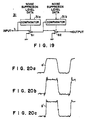
- the signal g (Fig. 18g) has a waveform such that the gradient is steep and the emphasis of the small amplitude edge has been completed, even when the noise suppression level of the noise suppression circuit 31 is caused to be larger than that of the conventional circuit, there is no possibility that an adverse effect as in the conventional circuit does not occur, with the result that the noise suppression level is caused to be sufficiently large, thus permitting both the small amplitude level and the large amplitude level of the waveform to be emphasized.
- the noise amplitude hardly becomes large in the output signal of the limiter 25 and it is possible to allow the noise suppression level of the noise suppression circuit 31 to be larger than that of the conventional circuit, noise is hardly included in the output signal i , but only the large amplitude edge component is included therein. Accordingly, the output signal j of which noise amplitude hardly becomes large is obtained.
- Fig. 21 is a block diagram illustrating a fourth video signal processing circuit to aid understanding of the present invention.
- components identical to those in Fig. 17 are represented with the same reference numerals, respectively, and their explanation will be omitted.
- a delay circuit 213 has a delay time of 2 ⁇ t. By delaying an input signal by the time 2 ⁇ t, this circuit 21 produces a signal b to deliver it to a comparator 22 and switches S1 and S2.
- Such a circuit configuration is used in the case where it is not desirable in view of the problem of fan out that the high frequency range emphasis filter or the high-pass filter and the delay circuit for obtaining the signal b are commonly used. Since the operation and the advantage of this circuit are the same as those in the third embodiment, its explanation will be omitted.
- Fig. 22 is a block diagram of a circuit combining the third and fourth video signal processing circuits.
- the output of the high frequency component extraction circuit 42 is inputted to the noise suppression circuit 31 and the output of the noise suppression circuit 31 is inputted to the adder circuit 32 together with the output of the limiter 25.
- the output of this video signal processing circuit is taken out from the output terminal of the adder circuit 32.
- Fig. 23 is a detailed circuit diagram in which the circuit configuration shown in Fig. 22 is realized with an analogue circuit.
- the high frequency range emphasis circuit 41 has an identical arrangement of the high frequency range emphasis filter 27 shown in Fig. 16.
- the high frequency range component extraction circuit 42 has an arrangement in which transistors Q51 and Q52, capacitors C51-C53, resistors R51-R56 and adjustable resistors VR51 and VR52, which form an adder circuit, and these correspond to transistors Q4 and Q5, capacitors C3-C5, resistors R13-R18 and adjustable resistors VR1 and VR2 of the high frequency band emphasis circuit.
- the emitter terminal of the transistor Q52 is connected to the noise suppression circuit 31, which form an adder of the same arrangement as mentioned above.
- the noise suppression circuit is composed of serially-connected a capacitor C57, adjustable resistor VR54 and a pair of diodes D1, D2 connected in parallel with those polarities reversed.
- the output terminal of the noise suppression circuit is connected to the emitter terminal of the transistor Q53 in the adder 32.
- the output of the amplifier 29 is also inputted to the adder 32 through a variable resistor 53 and a capacitor C54.
- the adder 32 is composed of transistors Q53 and Q54, capacitor C55, and resistors R57-R61, which are the same as the above-mentioned adder in the high frequency range emphasis circuit 41.
- signals selected by the switches S1 and S2 in the circuit shown in Fig. 17 or 21 may be opposite to those in the above-mentioned embodiments, thus to eliminate the lower and upper side waveform ringings at the limiters 24 and 25, respectively.
- the coefficients k1 and k2 of the respective multipliers 281 and 282 are not limited to those in the above-mentioned embodiment.
- Fig. 24 shows an embodiment of the present invention, which relates to more universal case.
- the comparator 221 makes a level comparison between the data of input signal a and that of the signal b which is the output signal of DL 212 with a delay of 2 ⁇ t to effect switching of the terminals A and B of the switch S1 so as to select a signal data of higher level of the signals a and b, and to effect switching of the terminals C and D of the switch S3 so as to select a signal data of lower level of the signals a and b .
- the comparator 222 makes a level comparison between the selected higher signal data and that of an output signal of DL 211 with a delay of ⁇ t to effect switching of the terminals E and F of the switch S2 so as to select the signal data of highest level among the input signal, the signal with 1 ⁇ t and the signal with 2 ⁇ t.
- the comparator 223 compares the level of selected lower signal to the level of an output signal of DL 211 with a delay of ⁇ t to effect switching of the terminals G and H of the switch S4 so as to select the signal data of lowest level among the input signal, the signal with 1 ⁇ t and the signal with 2 ⁇ t.
- the selected highest (maximum) signal is inputted to the limiter 24 as its threshold level and the selected lowest (minimum) signal is inputted to the limiter 25 as its threshold level.
- Fig. 25h shows a waveform which is obtained by emphasizing high frequency range of the signal shown in Fig. 25c
- Fig. 25i shows a waveform which is obtained by limiting the signal shown in Fig. 25h applying the signal shown in Fig. 25f as a higher threshold level
- Fig. 25j shows an waveform which is obtained by limiting the signal shown in Fig. 25i applying the signal shown in Fig. 25g as a lower threshold level.
- Fig. 25l shows the maximum signal obtained from signals shown in Fig. 25a, 25c and 25e and Fig. 25m shows a signal obtained when the signal shown in Fig. 25h is limited by using the signal shown in Fig. 25l as a highest threshold level.
- Fig. 25n shows a signal obtained when the signal shown in fig. 25m is limited by using the signal shown in Fig. 25g as a lowest threshold level. As seen from in Fig. 25n the dip of level is decreased.
- the dip is further decreased as shown in fig. 25o.
- the limiting is performed using the maximum and minimum signals obtained from signals having different delays, the waveform of an output signal is improved.
Landscapes
- Engineering & Computer Science (AREA)
- Signal Processing (AREA)
- Multimedia (AREA)
- Picture Signal Circuits (AREA)
Claims (10)
- Videosignal-Verarbeitungsschaltung zur Aperturkorrektur oder Bildqualität-Wiederherstellung, enthaltend eine Verzögerungseinrichtung, welche Verarbeitungsschaltung enthält:
eine Hochfrequenzbereich-Emphasiseinrichtung (23, 27, 41) zum Erzeugen eines Signals mit einem angehobenen hohen Frequenzbereich, das dadurch erhalten wird, daß ein Eingangsvideosignal um eine vorbestimmte Verzögerungszeit verzögert und ein hoher Frequenzbereich des Eingangsvideosignals angehoben wird;
eine Vielzahl von Verzögerungseinrichtungen (21, 27, 41), die seriell zum Erzeugen von drei oder mehreren Signalen mit verschiedenen Verzögerungszeiten verbunden sind;
eine Selektoreinrichtung (22, 28) zum Betwirken eines Pegelvergleiches zwischen dem Eingangsvideosignal und den verzögerten Signalen zum separaten Herausnehmen von Signaldaten mit einem maximalen Pegel und von solchen mit einem minimalen Pegel;
einen ersten Begrenzer (24) zum Begrenzen des Signals mit dem angehobenen hohen Frequenzbereich durch Vergleichen mit dem vom Selektor ausgewählten Signal maximalen oder minimalen Pegels unter Verwendung des maximalen oder minimalen Pegels als einen ersten Schwellenwertpegel; und
einen zweiten Begrenzer (25) zum Begrenzen eines Ausgangssignals des ersten Begrenzers durch Vergleichen mit dem vom Selektor ausgewählten Signal minimalen oder maximalen Pegels unter Verwendung des minimalen oder maximalen Pegels als einen zweiten Schwellenwertpegel. - Videosignal-Verarbeitungsschaltung nach Anspruch 1, bei der die Verzögerungseinrichtung aus zwei Verzögerungsschaltungen besteht, die Signale erzeugen, die dadurch erhalten werden, daß das Eingangsvideosignal um die vorbestimmte Verzögerungszeit bzw. um eine Verzögerungszeit verzögert wird, die zweimal größer als die vorbestimmte Verzögerungszeit ist, und die Selektoreinrichtung einen Pegelvergleich zwischen dem Eingangsvideosignal und Ausgangssignalen der Verzögerungseinrichtung ausführt, um separat herauszunehmen Signale mit höherem Pegel und niedrigerem Pegel.
- Videosignal-Verarbeitungsschaltung nach Anspruch 1, bei der die Hochfrequenzbereich-Emphasiseinrichtung aus einem Hochfrequenzbereich-Emphasisfilter besteht und die Verzögerungseinrichtung aus Verzögerungsschaltungen besteht, die von dem Hochfrequenzbereich-Emphasisfilter separat vorgesehen sind.
- Videosignal-Verarbeitungsschaltung nach Anspruch 1, bei der die Hochfrequenzbereich-Emphasiseinrichtung aus einem Hochfrequenzbereich-Emphasisfilter besteht und die Verzögerungseinrichtungen aus Verzögerungsschaltungen bestehen, die einen mit dem Hochfrequenzbereich-Emphasisfilter gemeinsam benutzten Schaltungsaufbau haben.
- Videosignal-Verarbeitungsschaltung nach Anspruch 2, bei der die Selektoreinrichtung einen Vergleicher, einen ersten Schalter und einen zweiten Schalter enthält, die von einem Ausgangssignal des Vergleichers angesteuert werden, der erste Schalter entweder das Eingangsvideosignal oder das Signal mit der zweifachen Verzögerung auswählt, um das ausgewählte Signal dem ersten Begrenzer zuzuführen, und der zweite Schalter entweder das Eingangsvideosignal oder das Signal mit der zweifachen Verzögerung auswählt, um das ausgewählte Signal dem zweiten Begrenzer zuzuführen.
- Videosignal-Verarbeitungsschaltung nach Anspruch 1, ferner enthaltend:
eine Hochfrequenzkomponenten-Extraktionseinrichtung (42) zum Erzeugen eines extrahierten Signals mit einer hohen Frequenzkomponente, das dadurch erhalten wird, daß das Eingangsvideosignal um die vorbestimmte Zeit verzögert und die hohe Frequenzkomponente des Eingangsvideosignals herausgenommen wird;
eine Rauschunterdrückungseinrichtung (31) zum Bewirken einer Rauschunterdrückung der extrahierten hohen Frequenzkomponente; und
eine Addiereinrichtung (32) zum Durchführen einer Addition eines Ausgangs der Rauschunterdrückungseinrichtung und eines Ausgangs des zweiten Begrenzers. - Videosignal-Verarbeitungsschaltung nach Anspruch 6, bei der die Verzögerungseinricntung aus zwei Verzögerungsschaltungen besteht, die Signale erzeugen, die dadurch erhalten werden, daß das Eingangsvideosignal um die vorbestimmte Verzögerungszeit bzw. eine Verzögerungszeit verzögert wird, die zweimal größer als die vorbestimmte Verzögerungszeit ist, und die Selektoreinrichtung einen Pegelvergleich zwischen dem Eingangsvideosignal und Ausgangssignalen der Verzögerungseinrichtung ausführt, um Signale höheren Pegels und niedrigeren Pegels separat herauszunehmen.
- Videosignal-Verarbeitungschaltung nach Anspruch 6, bei der die Hochfrequenzbereich-Emphasiseinrichtung aus einem Hochfrequenzbereich-Emphasisfilter besteht, die Hochfrequenzkomponenten-Extraktionseinrichtung aus einem Hochpaßfilter besteht und die Verzögerungseinrichtung aus Verzögerungsschaltungen gebildet ist, die von dem Hochfrequenzbereich-Emphasisfilter und dem Hochpaßfilter separat vorgesehen sind.
- Videosignal-Verarbeitungsschaltung nach Anspruch 6, bei der die Hochfrequenzbereich-Emphasiseinrichtung aus einen Hochfrequenzbereich-Emphasisfilter besteht, die Frequenzkomponenten-Extraktionsschaltung aus einem Hochpaßfilter besteht und die Verzögerungseinrichtung aus Verzögerungsschaltungen besteht, die einen mit dem Hochfrequenzbereich-Enphasisfilter und dem Hochpaßfilter gemeinsam benutzten Schaltungsaufbau haben.
- Videosignal-Verarbeitungsschaltung nach Anspruch 7, bei der die Selektoreinrichtung einen Vergleicher, einen ersten Schalter und einen zweiten Schalter enthält, die von einem Ausgangssignal des Vergleichers angesteuert werden, der erste Schalter entweder das Eingangsvideosignal oder das Signal mit der zweifachen Verzögerung auswählt, um es dem ersten Begrenzer zuzuführen, und der zweite Schalter entweder das Eingangsvideosignal oder das Signal mit der zweifachen Verzögerung auswählt, um es dem zweiten Begrenzer zuzuführen.
Applications Claiming Priority (4)
| Application Number | Priority Date | Filing Date | Title |
|---|---|---|---|
| JP217839/86 | 1986-09-16 | ||
| JP61217840A JPS6373775A (ja) | 1986-09-16 | 1986-09-16 | デジタルビデオ信号処理回路 |
| JP61217839A JPS6373774A (ja) | 1986-09-16 | 1986-09-16 | デジタルビデオ信号処理回路 |
| JP217840/86 | 1986-09-16 |
Publications (3)
| Publication Number | Publication Date |
|---|---|
| EP0260913A2 EP0260913A2 (de) | 1988-03-23 |
| EP0260913A3 EP0260913A3 (en) | 1989-09-27 |
| EP0260913B1 true EP0260913B1 (de) | 1993-07-21 |
Family
ID=26522234
Family Applications (1)
| Application Number | Title | Priority Date | Filing Date |
|---|---|---|---|
| EP87308106A Expired - Lifetime EP0260913B1 (de) | 1986-09-16 | 1987-09-14 | Schaltung zur Verarbeitung vom Videosignal |
Country Status (4)
| Country | Link |
|---|---|
| US (1) | US4853783A (de) |
| EP (1) | EP0260913B1 (de) |
| KR (1) | KR910008922B1 (de) |
| DE (1) | DE3786623T2 (de) |
Families Citing this family (7)
| Publication number | Priority date | Publication date | Assignee | Title |
|---|---|---|---|---|
| GB2234133B (en) * | 1989-07-14 | 1993-11-10 | Mitsubishi Electric Corp | Video signal processing apparatus |
| US5546135A (en) * | 1992-02-28 | 1996-08-13 | Matsushita Electric Industrial Co., Ltd. | Contour restoration apparatus |
| US5369446A (en) * | 1992-04-30 | 1994-11-29 | Thomson Consumer Electronics, Inc. | Video signal processor employing edge replacement, preshoots and overshoots for transient enhancement |
| US6002797A (en) * | 1994-06-22 | 1999-12-14 | Hitachi, Ltd. | Apparatus for detecting position of featuring region of picture, such as subtitle or imageless part |
| KR0141782B1 (ko) * | 1994-09-10 | 1998-06-15 | 구자홍 | 영상선명화장치 |
| US6441866B1 (en) * | 1999-01-14 | 2002-08-27 | Omnivision Technologies, Inc. | Edge enhancement with background noise suppression in video image processing |
| US20060221240A1 (en) * | 2003-12-10 | 2006-10-05 | Koninklijke Philips Electronics N.V. | Method and apparatus for generating thin lines in video images |
Family Cites Families (2)
| Publication number | Priority date | Publication date | Assignee | Title |
|---|---|---|---|---|
| US3878323A (en) * | 1968-05-01 | 1975-04-15 | Image Analysing Computers Ltd | Detecting devices for image analysis systems |
| JPS58219872A (ja) * | 1982-06-15 | 1983-12-21 | Pioneer Electronic Corp | 輪郭補正回路 |
-
1987
- 1987-09-14 EP EP87308106A patent/EP0260913B1/de not_active Expired - Lifetime
- 1987-09-14 DE DE87308106T patent/DE3786623T2/de not_active Expired - Fee Related
- 1987-09-15 KR KR1019870010183A patent/KR910008922B1/ko not_active Expired
- 1987-09-16 US US07/096,997 patent/US4853783A/en not_active Expired - Lifetime
Also Published As
| Publication number | Publication date |
|---|---|
| EP0260913A2 (de) | 1988-03-23 |
| KR910008922B1 (ko) | 1991-10-24 |
| KR880004462A (ko) | 1988-06-04 |
| US4853783A (en) | 1989-08-01 |
| EP0260913A3 (en) | 1989-09-27 |
| DE3786623T2 (de) | 1993-12-02 |
| DE3786623D1 (de) | 1993-08-26 |
Similar Documents
| Publication | Publication Date | Title |
|---|---|---|
| US4030121A (en) | Video crispener | |
| EP1051043B1 (de) | Bildqualitätskorrekturschaltung | |
| US4860104A (en) | Noise eliminating apparatus of a video signal utilizing a recursive filter having spatial low pass and high pass filters | |
| US4232330A (en) | Method and system for separating the chrominance and luminance signals in color television signals having quadrature-modulated chrominance subcarriers | |
| GB2112246A (en) | Carrier colour signal processing circuits | |
| US4823190A (en) | Apparatus for enhancing contours of television signal | |
| EP0558017B1 (de) | Konturrekonstruktionsgerät | |
| US4571613A (en) | Noise reduction circuit for a video signal using a feedback type comb filter and an equalizer circuit | |
| US4626927A (en) | Recording and reproducing apparatus for recording and reproducing a carrier chrominance signal with pre-emphasis and de-emphasis | |
| US4853783A (en) | Video signal processing circuit | |
| US4916527A (en) | Luminance signal/color signal separation circuit | |
| GB2251353A (en) | Noise reduction | |
| EP0514196B1 (de) | Bildqualitätsverbesserungsschaltung zur Bildkontourkompensation | |
| EP0128707B1 (de) | Signalverarbeitungsvorrichtung für ein Videosignal | |
| US4750033A (en) | Comb filter, chrominance and luminance signal separating circuit for modifying the level-frequency characteristic of the luminance signal | |
| US5912702A (en) | Video camera and image enhancing apparatus | |
| US5159442A (en) | Color signal processing apparatus | |
| KR0185930B1 (ko) | 신호레벨에 따라 임계레벨을 설정하는 영상신호의 노이즈 제거장치 | |
| EP0268332B1 (de) | Verfahren und Schaltung zur Erzeugung eines anpassungsfähigen Anhebungssignals zur Vergrösserung der Schärfe eines Videosignals | |
| KR930003968B1 (ko) | 영상신호의 윤곽 보정회로 | |
| JP2789601B2 (ja) | 非線形信号処理装置 | |
| JP2555799B2 (ja) | 画質改善装置 | |
| JPH04294687A (ja) | 画質改善装置 | |
| JPS6373774A (ja) | デジタルビデオ信号処理回路 | |
| JPH03120963A (ja) | 輪郭補正器 |
Legal Events
| Date | Code | Title | Description |
|---|---|---|---|
| PUAI | Public reference made under article 153(3) epc to a published international application that has entered the european phase |
Free format text: ORIGINAL CODE: 0009012 |
|
| AK | Designated contracting states |
Kind code of ref document: A2 Designated state(s): DE FR GB |
|
| PUAL | Search report despatched |
Free format text: ORIGINAL CODE: 0009013 |
|
| AK | Designated contracting states |
Kind code of ref document: A3 Designated state(s): DE FR GB |
|
| 17P | Request for examination filed |
Effective date: 19891024 |
|
| 17Q | First examination report despatched |
Effective date: 19911210 |
|
| GRAA | (expected) grant |
Free format text: ORIGINAL CODE: 0009210 |
|
| AK | Designated contracting states |
Kind code of ref document: B1 Designated state(s): DE FR GB |
|
| ET | Fr: translation filed | ||
| REF | Corresponds to: |
Ref document number: 3786623 Country of ref document: DE Date of ref document: 19930826 |
|
| PLBE | No opposition filed within time limit |
Free format text: ORIGINAL CODE: 0009261 |
|
| STAA | Information on the status of an ep patent application or granted ep patent |
Free format text: STATUS: NO OPPOSITION FILED WITHIN TIME LIMIT |
|
| 26N | No opposition filed | ||
| PGFP | Annual fee paid to national office [announced via postgrant information from national office to epo] |
Ref country code: DE Payment date: 20000904 Year of fee payment: 14 |
|
| PGFP | Annual fee paid to national office [announced via postgrant information from national office to epo] |
Ref country code: FR Payment date: 20000912 Year of fee payment: 14 |
|
| PGFP | Annual fee paid to national office [announced via postgrant information from national office to epo] |
Ref country code: GB Payment date: 20000913 Year of fee payment: 14 |
|
| PG25 | Lapsed in a contracting state [announced via postgrant information from national office to epo] |
Ref country code: GB Free format text: LAPSE BECAUSE OF NON-PAYMENT OF DUE FEES Effective date: 20010914 |
|
| REG | Reference to a national code |
Ref country code: GB Ref legal event code: IF02 |
|
| GBPC | Gb: european patent ceased through non-payment of renewal fee |
Effective date: 20010914 |
|
| PG25 | Lapsed in a contracting state [announced via postgrant information from national office to epo] |
Ref country code: DE Free format text: LAPSE BECAUSE OF NON-PAYMENT OF DUE FEES Effective date: 20020501 |
|
| PG25 | Lapsed in a contracting state [announced via postgrant information from national office to epo] |
Ref country code: FR Free format text: LAPSE BECAUSE OF NON-PAYMENT OF DUE FEES Effective date: 20020531 |
|
| REG | Reference to a national code |
Ref country code: FR Ref legal event code: ST |