EP0260889B1 - Vollduplex-Modem - Google Patents
Vollduplex-Modem Download PDFInfo
- Publication number
- EP0260889B1 EP0260889B1 EP87308048A EP87308048A EP0260889B1 EP 0260889 B1 EP0260889 B1 EP 0260889B1 EP 87308048 A EP87308048 A EP 87308048A EP 87308048 A EP87308048 A EP 87308048A EP 0260889 B1 EP0260889 B1 EP 0260889B1
- Authority
- EP
- European Patent Office
- Prior art keywords
- signals
- transmit
- receive
- data
- reception
- Prior art date
- Legal status (The legal status is an assumption and is not a legal conclusion. Google has not performed a legal analysis and makes no representation as to the accuracy of the status listed.)
- Expired - Lifetime
Links
- 238000000034 method Methods 0.000 claims abstract description 56
- 239000000872 buffer Substances 0.000 claims abstract description 32
- 230000005540 biological transmission Effects 0.000 claims description 31
- 230000015654 memory Effects 0.000 claims description 20
- 230000000977 initiatory effect Effects 0.000 claims description 8
- 230000004044 response Effects 0.000 claims description 5
- 238000005070 sampling Methods 0.000 claims 2
- 230000001360 synchronised effect Effects 0.000 claims 2
- 238000010586 diagram Methods 0.000 description 6
- 230000007704 transition Effects 0.000 description 5
- 238000006243 chemical reaction Methods 0.000 description 2
- 230000002457 bidirectional effect Effects 0.000 description 1
- 230000003090 exacerbative effect Effects 0.000 description 1
- 238000001914 filtration Methods 0.000 description 1
- 238000012986 modification Methods 0.000 description 1
- 230000004048 modification Effects 0.000 description 1
- 230000008054 signal transmission Effects 0.000 description 1
- 230000001629 suppression Effects 0.000 description 1
Images


Classifications
-
- H—ELECTRICITY
- H04—ELECTRIC COMMUNICATION TECHNIQUE
- H04L—TRANSMISSION OF DIGITAL INFORMATION, e.g. TELEGRAPHIC COMMUNICATION
- H04L5/00—Arrangements affording multiple use of the transmission path
- H04L5/14—Two-way operation using the same type of signal, i.e. duplex
- H04L5/143—Two-way operation using the same type of signal, i.e. duplex for modulated signals
Definitions
- the present invention relates generally to signal processors in data transmission and receiving systems, such as a modulator-demodulator (modem), and more specifically, to the time-shared use of a single processor performing transmit-side and receive-side procedures in a full-duplex modem.
- modem modulator-demodulator
- DAC digital-to-analog conversion
- ADC analog-to-digital conversion
- filtering digital and analog filtering
- noise suppression and the like.
- separate control of the transmitter-side and the receiver-side are employed to execute these procedures.
- full-duplex operation of a modulator-demodulator (modem) in which simultaneous bidirectional data transmission; i.e., transmission and reception of data signals at the same time.
- modems employ separate microprocessors, one for the transmit-side and one for the receive-side.
- Provision of two separate microprocessors which duplicate each other's capability is a wasteful, expensive and ill-advised from a reliability standpoint. Exacerbating this situation, is the case of a single integrated circuit which is to house all elements of a modem, i.e., a single-chip modem. In this case valuable die space is wasted by the use of two processors.
- the present invention provides a method of scheduling full-duplex transmission and reception of data by a single processor in a modem activated by a receive-enable signal and a transmit-enable signal and having a transmit buffer memory, said method comprising the steps of:
- the present invention also provides a method of scheduling full-duplex transmission and reception of data by a single processor in a modem activated by a receive-enable signal and a transmit-enable signal and having a receive buffer memory, said method comprising the steps of:
- Timing of the transmit- and receive-side signal processing procedures by the single processor is controlled by reception of transmit-enable and receive-enable signals, respectively.
- actual execution of the transmit-and receive-side procedures varies according to the time-sharing procedure employed by the processor.
- transmission takes precedence over reception of data and reception of a transmit-enable signal interrupts an on-going reception of data and the latter continues only after transmission is completed.
- reception of a receive-enable signal during transmission does not interrupt the on-going transmission of data and reception begins only after transmission is completed.
- a single-chip modem employs a single processor of the present invention.
- Fig. 1 illustrates two modulator/demodulators (modems) connected to a telephone line.
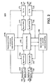
- Fig. 2 is a block diagram of a modem employing a single processor of the present invention.
- Fig. 3A and Fig. 3B are timing diagrams of the transmit- and receive-side, respectively, of a modem employing a single processor of the present invention.
- Fig. 4 is a state diagram illustrating the time-sharing procedure used by a modem employing a single processor of the instant invention.
- Fig. 1 Shown in Fig. 1 is a typical utilization of two modulator-demodulators (modems) 10 and 12 on a telephone line 14.
- Hybrid circuits 16 and 18 include inductor coils and balancing network, as is known to those skilled in the art, and modems 10 and 12 connect to telephone line 14 via hybrid circuit 16 and 18, respectively.
- Each modem shown in Fig. 1 converts digital data signals (TD) applied to a signal line 20 or 22 into analog signals (TC) generated on a signal line 24 or 26 to be transmitted on telephone line 14. Each modem also converts analog data signals (RC) applied to a signal line 28 or 30 into digital signals (RD) generated on a signal line 32 or 34. Receive-enable and transmit-enable signals are employed by the modems to initiate reception and transmission of signals, as is well known to those skilled in the art.
- modem 10 will extract timing information from the analog signal received from modem 12.
- Modem 10 generates therefrom a receive-enable signal phase-locked to the transmit-enable signal at modem 12.
- this receive-enable signal of modem 10 is not phase-locked to the transmit-enable signal of modem 10.
- the transmit-enable signal of modem 10 is derived from an oscillator internal to modem 10 or from an external clock source.
- Modems 10 and 12 employ microprocessors to perform various receive-side and transmit-side procedures initiated by the receive-enable and transmit-enable signals, as will be explained in connection with Fig. 2.
- FIG. 2 A block diagram of a modem 100 employing a single processor 102 is shown in Fig. 2.
- Various signal lines are shown connecting the elements of modem 100.
- Control signals generated by the elements shown in Fig. 2, especially the processor 102, are conducted along lines not shown in Fig. 2.
- Such control signals are well known to those skilled in the art.
- Also not shown in Fig. 2 is a memory used to store programs and data employed by the single processor 102 of the present invention. Such memories are also well known in the art.
- a transmit data portion 104 of modem 100 formats the TD data signals received on line 20 and sends the formatted data to a buffer 106 synchronously at a rate Tx1.
- the clock signal Tx1 is generated by a transmitter clock generator portion 108.
- the processor of 102 will read the information in buffer 106 asynchronously, execute the transmitter-side procedures (stored in the memory referred to in the preceding paragraph) and send N T digitized samples of the analog signals (TD) to a buffer 110.
- Data is read from buffer 110 synchronously at a rate N T times Tx1, converted to an analog signal (TC) and generated on the signal line 24 by a digital-to-analog (D/A) portion 112.
- An analog-to-digital (A/D) portion 114 converts the analog signals RC received on line 28 into digital values which are stored in a buffer 116 synchronously at a rate of N R times Rx1.
- the clock signal Rx1 is generated by a receiver clock generator 118 and N R is the number of digital values stored in buffer 116.
- the processor 102 roads values from buffer 116 asynchronously, executes the receiver-side procedures (stored in the memory referred to earlier) and sends the resulting data to a buffer 120. Data is read from buffer 120 synchronously at a rate of Rx1, formatted and transmitted as RD signals on line 32 by a receive data portion 122.
- a routine in the receiver-side procedures will cause processor 102 to send a control signal to the receiver clocks generator 118 to phase-lock the receiver-enable signal with the transmit-enable signal of the other modem in the connection.
- buffer 106 and buffer 120 will be one word. This follows from the fact that the receiver-side procedure will run once every period of the Rx1 clock and the transmittal-side procedure will run once every period of the Tx1 clock.
- the instant invention is a method for responding to the receive-enable and transmit-enable signals which allows for buffer 110 and buffer 116 to be very small while still causing no data loss due to overflow or underflow.
- the delay shown in Fig. 3A as ⁇ T is a constant, the size of buffer 110 would be N T which is a minimum.
- the delay shown in Fig. 3B and R is a constant, the size of buffer 116 would be N R which is minimum.
- the constraint of having only one processor 102 it is necessary to vary the values of ⁇ T and ⁇ R .
- t1 indicates transmit-enable signal received by processor 102
- t1+ ⁇ T indicates transmitter code begins execution
- t2 indicates receive-enable signal received by processor 102
- t2+ ⁇ R indicates when receiver code begins execution.
Landscapes
- Engineering & Computer Science (AREA)
- Signal Processing (AREA)
- Computer Networks & Wireless Communication (AREA)
- Communication Control (AREA)
- Interface Circuits In Exchanges (AREA)
- Bidirectional Digital Transmission (AREA)
- Polysaccharides And Polysaccharide Derivatives (AREA)
- Telephonic Communication Services (AREA)
Claims (6)
- Verfahren zum Organisieren des Vollduplex-Sendens und -Empfangens von Daten durch einen einzelnen Prozessor in einem Modem, das durch ein Empfangsfreigabesignal und ein Sendefreigabesignal aktiviert wird und einen Sendepufferspeicher (106) aufweist, wobei das Verfahren die folgenden Schritte aufweist:a) Initiieren des Empfangs der Daten durch den Prozessor in Reaktion auf das Empfangsfreigabesignal,b) Empfangen des Sendefreigabesignals durch den Prozessor,c) Zwischenspeichern einer Sendeinformation in einem Sendepufferspeicher während einer variablen Sendeverzögerung, wobei die Menge der in dem Sendepufferspeicher zu speichernden Informationen der Differenz zwischen dem Maximal- und dem Minimalwert der variablen Sendeverzögerung entspricht,d) Unterbrechen des Empfangs der Daten und Initiieren des Sendens der Daten nach der variablen Sendeverzögerung, unde) Wiederaufnehmen des Empfangs der Daten nach Abschluß des Sendens.
- Organisationsverfahren nach Anspruch 1, gekennzeichnet durch das Verwenden eines Sendepufferspeichers (106) mit einer Speicherkapazität von


- Verfahren zum Organisieren des Vollduplex-Sendens und -Empfangens von Daten durch einen einzelnen Prozessor in einem Modem, das durch ein Empfangsfreigabesignal und ein Sendefreigabesignal aktiviert wird und einen Empfangspufferspeicher (106) aufweist, wobei das Verfahren die folgenden Schritte aufweist:a) Initiieren des Sendens der Daten durch den Prozessor in Reaktion auf das Sendefreigabesignal,b) Empfangen des Empfangsfreigabesignals durch den Prozessor,c) Zwischenspeichern von Empfangsinformationen in einem Empfangspufferspeicher (106) während einer Empfangsverzögerung, wobei die Menge der in dem Empfangspufferspeicher zu speichernden Informationen der Differenz zwischen dem Maximal- und dem Minimalwert der variablen Empfangsverzögerung entspricht,d) Unterbrechen des Sendens der Daten und Initiieren des Empfangs der Daten nach der variablen Empfangsverzögerung, unde) Wiederaufnehmen des Sendens der Daten nach Abschluß des Empfangs.
- Organisationsverfahren nach Anspruch 3, gekennzeichnet durch das Verwenden eines Empfangspufferspeichers mit einer Speicherkapazität von


- Vollduplex-Modem zum Empfang digitaler Datensignale (TD), die als analoge Datensignale (TC) zu senden sind, und zum Empfangen von analogen Datensignalen (RC), die in empfangene digitale Datensignale (RD) umzusetzen sind, mit:- einer Einrichtung (108) zum Erzeugen mehrerer Transmittertaktsignale;- einer Einrichtung (118) zum Erzeugen mehrerer Empfängertaktsignale;- einer auf eines der Transmittertaktsignale reagierenden Einrichtung (10) zum Empfang der TD-Signale und zum synchronen Erzeugen von Signalen aus diesen mit einer vorbestimmten Rate Tx1;- einer ersten Einrichtung (106) zum Zweischenspeichern von NT der aus den TD-Signalen erzeugten synchronen Signale;- einer auf eines der Empfängertaktsignale hin reagierenden Einrichtung (114) zum Empfangen der RC-Signale und zum synchronen Erzeugen von digitalen Signalen aus diesen mit einem vorbestimmten Vielfachen NR einer vorbestimmten Rate Rx1;- einer zweiten Einrichtung (116) zum Zwischenspeichern des vorbestimmten Vielfachen NR der aus den RC-Signalen erzeugten synchronen Signale;- einer Speichereinrichtung zum Speichern von Programmen und Daten;- einer betriebsmäßig mit der Speichereinrichtung verbundenen, auf wenigstens eines der Transmittertaktsignale und auf wenigstens eines der Empfängertaktsignale reagierenden programmierbaren digitalen Prozessoreinrichtung (102) zum Abtasten der aus den TD-Signalen erzeugten zwischengespeicherten Signale, zum Ausführen eines sendeseitigen Signalverarbeitungsvorgangs an diesen und zum Erzeugen digitalisierter Sendedaten aus diesen, zum Abtasten der aus den RC-Signalen erzeugten zwischengespeicherten Signale, zum Ausführen eines empfangsseitigen Signalverarbeitungsvorgangs an diesen und zum Erzeugen digitalisierter Empfangsdaten aus diesen;- einer auf eines der Transmittertaktsignale reagierenden dritten Einrichtung (110) zum Zwischenspeichern der digitalisierten Sendesignale;- einer auf eines der Transmittertaktsignale reagierenden Einrichtung (112) zum Umwandeln der zwischengespeicherten digitalisierten Sendesignale in die analogen Datensignale (TC);- einer auf eines der Empfängertaktsignale reagierenden vierten Einrichtung (120) zum Zwischenspeichern der digitalisierten Empfangssignale;- einer auf eines der Empfängertaktsignale reagierenden Einrichtung (122) zum Empfangen der zwischengespeicherten digitalisierten Empfangssignale und zum synchronen Erzeugen der empfangenen digitalen Datensignale (RD) aus diesen mit der vorbestimmten Rate Rx1;- wodurch die programmierbare digitale Prozessoreinrichtung die sendeseitige und die empfangsseitige Signalverarbeitung in bezug auf die Zeit gemäß einer vorbestimmten Organisation durchführt.
- Vollduplex-Modem nach Anspruch 5, zum Empfangen eines Sendefreigabesignals und eines Empfangsfreigabesignals, dadurch gekennzeichnet, daß die programmierbare digitale Prozessoreinrichtung ferner auf die Sende- und Empfangsfreigabesignale reagiert, wobei die Prozessoreinrichtung eine Maximal- bzw. eine Minimalverzögerung


Priority Applications (1)
| Application Number | Priority Date | Filing Date | Title |
|---|---|---|---|
| AT87308048T ATE96259T1 (de) | 1986-09-19 | 1987-09-11 | Vollduplex-modem. |
Applications Claiming Priority (2)
| Application Number | Priority Date | Filing Date | Title |
|---|---|---|---|
| US910111 | 1978-05-30 | ||
| US06/910,111 US4943942A (en) | 1986-09-19 | 1986-09-19 | Full-duplex modem using a single processor |
Publications (3)
| Publication Number | Publication Date |
|---|---|
| EP0260889A2 EP0260889A2 (de) | 1988-03-23 |
| EP0260889A3 EP0260889A3 (en) | 1990-02-07 |
| EP0260889B1 true EP0260889B1 (de) | 1993-10-20 |
Family
ID=25428326
Family Applications (1)
| Application Number | Title | Priority Date | Filing Date |
|---|---|---|---|
| EP87308048A Expired - Lifetime EP0260889B1 (de) | 1986-09-19 | 1987-09-11 | Vollduplex-Modem |
Country Status (6)
| Country | Link |
|---|---|
| US (1) | US4943942A (de) |
| EP (1) | EP0260889B1 (de) |
| JP (1) | JPH0728322B2 (de) |
| AT (1) | ATE96259T1 (de) |
| DE (1) | DE3787857T2 (de) |
| ES (1) | ES2044949T3 (de) |
Families Citing this family (12)
| Publication number | Priority date | Publication date | Assignee | Title |
|---|---|---|---|---|
| EP0293704A3 (de) * | 1987-06-01 | 1989-02-15 | Hoechst Celanese Corporation | Aufzeichnungsmaterial mit einer wasserlöslichen Kontrastverstärkungsschicht |
| CA2056046C (en) * | 1990-11-27 | 1996-02-27 | Keisuke Okuzono | Interface circuit between a plurality of transmission line and a high bit rate data terminal equipment |
| US5197128A (en) * | 1991-03-04 | 1993-03-23 | Hewlett-Packard Company | Modular interface |
| US5524252A (en) * | 1991-04-19 | 1996-06-04 | International Business Machines Corporation | Personal computer system combined with an adapter for networks having varying characteristics, and adapter for coupling a personal computer to such networks |
| US5414740A (en) * | 1992-12-17 | 1995-05-09 | International Business Machines Corporation | Synchronous communication system having multiplexed information transfer and transition phases |
| US5678059A (en) * | 1994-02-18 | 1997-10-14 | Lucent Technologies Inc. | Technique for time-sharing a microprocessor between a computer and a modem |
| DE69615431T2 (de) * | 1995-03-15 | 2002-05-23 | Koninkl Philips Electronics Nv | Datenverarbeitungssystem zur Ausführung von Aufgaben verschiedener Prioritäten und dieses System enthaltendes Modem |
| US5995540A (en) * | 1997-01-08 | 1999-11-30 | Altocom, Inc. | System and method for reducing processing requirements of modem during idle receive time |
| US7383549B1 (en) | 1997-01-08 | 2008-06-03 | Broadcom Corporation | Processor sharing technique for communications and other data processing on a same processor |
| CN101142744A (zh) * | 2005-03-10 | 2008-03-12 | 新泻精密株式会社 | 半导体装置 |
| US7929456B2 (en) * | 2005-04-28 | 2011-04-19 | Nxp B.V. | Circuit for a communication device and method of controlling a transmission |
| US8106813B2 (en) * | 2010-01-27 | 2012-01-31 | Unnikrishna Sreedharan Pillai | Multichannel constant envelope orthogonal waveforms using receiver design |
Family Cites Families (3)
| Publication number | Priority date | Publication date | Assignee | Title |
|---|---|---|---|---|
| US4085449A (en) * | 1976-11-26 | 1978-04-18 | Paradyne Corporation | Digital modem |
| US4156796A (en) * | 1977-11-29 | 1979-05-29 | International Business Machines Corporation | Programmable data processing communications multiplexer |
| US4263670A (en) * | 1979-05-11 | 1981-04-21 | Universal Data Systems, Inc. | Microprocessor data modem |
-
1986
- 1986-09-19 US US06/910,111 patent/US4943942A/en not_active Expired - Fee Related
-
1987
- 1987-09-11 EP EP87308048A patent/EP0260889B1/de not_active Expired - Lifetime
- 1987-09-11 ES ES87308048T patent/ES2044949T3/es not_active Expired - Lifetime
- 1987-09-11 AT AT87308048T patent/ATE96259T1/de not_active IP Right Cessation
- 1987-09-11 DE DE87308048T patent/DE3787857T2/de not_active Expired - Lifetime
- 1987-09-17 JP JP62233635A patent/JPH0728322B2/ja not_active Expired - Lifetime
Also Published As
| Publication number | Publication date |
|---|---|
| JPS6387049A (ja) | 1988-04-18 |
| DE3787857D1 (de) | 1993-11-25 |
| EP0260889A2 (de) | 1988-03-23 |
| ES2044949T3 (es) | 1994-01-16 |
| JPH0728322B2 (ja) | 1995-03-29 |
| EP0260889A3 (en) | 1990-02-07 |
| DE3787857T2 (de) | 1994-04-21 |
| US4943942A (en) | 1990-07-24 |
| ATE96259T1 (de) | 1993-11-15 |
Similar Documents
| Publication | Publication Date | Title |
|---|---|---|
| EP0281307B1 (de) | Asynchrone Schnittstelle und Verfahren zur Datenkopplung zwischen einem Datenmodul und einem seriellen, asynchronen Pheripheriegerät | |
| US5727233A (en) | Byte-mode and burst-mode data transfer mechanism for a high-speed serial interface | |
| US4943942A (en) | Full-duplex modem using a single processor | |
| EP0762655A2 (de) | Hauptsignalverarbeitungskommunikationssystem unter Kompensation von Fehlausführung der Signalwartungsprozeduren | |
| US6108720A (en) | Echo canceling modem which dynamically switches sizes of sample buffer between first size for quick response time and second size for robustness to interrupt latency | |
| CA2060976C (en) | Dce and method for processing data received in a dce allowing multiple operating configurations | |
| JPH04334239A (ja) | データ・フォーマット検出回路 | |
| US5335337A (en) | Programmable data transfer timing | |
| US5586123A (en) | Interface and loopback circuit for character based computer peripheral devices | |
| US5799190A (en) | Communications coprocessor for realizing bidirectional isochronous communications link with host computer | |
| AU596459B2 (en) | Data transfer system having transfer discrimination circuit | |
| US5228129A (en) | Synchronous communication interface for reducing the effect of data processor latency | |
| US5940437A (en) | System and method for reducing the peak load on the processor of a block processing modem | |
| JPS6245255A (ja) | デ−タ受信方式 | |
| JPH08256164A (ja) | 通信システム | |
| JPH0591146A (ja) | シリアルデータ転送装置 | |
| US4490820A (en) | Reception system for key telephone system | |
| US6405268B1 (en) | Dynamic block processing in a host signal processing modem | |
| US7181555B2 (en) | Data communication apparatus, data communication method, and program | |
| JPH01309447A (ja) | 単線同期式通信方式 | |
| JPH08149157A (ja) | シリアルポート制御方法 | |
| GB1604485A (en) | Modem systems | |
| JPS59214351A (ja) | 直列信号送受信装置 | |
| KR20010009123A (ko) | 이원 및 티원 신호 변환장치 | |
| JPH0546515A (ja) | データ転送方式 |
Legal Events
| Date | Code | Title | Description |
|---|---|---|---|
| PUAI | Public reference made under article 153(3) epc to a published international application that has entered the european phase |
Free format text: ORIGINAL CODE: 0009012 |
|
| AK | Designated contracting states |
Kind code of ref document: A2 Designated state(s): AT BE CH DE ES FR GB GR IT LI LU NL SE |
|
| PUAL | Search report despatched |
Free format text: ORIGINAL CODE: 0009013 |
|
| AK | Designated contracting states |
Kind code of ref document: A3 Designated state(s): AT BE CH DE ES FR GB GR IT LI LU NL SE |
|
| 17P | Request for examination filed |
Effective date: 19900514 |
|
| 17Q | First examination report despatched |
Effective date: 19920312 |
|
| GRAA | (expected) grant |
Free format text: ORIGINAL CODE: 0009210 |
|
| AK | Designated contracting states |
Kind code of ref document: B1 Designated state(s): AT BE CH DE ES FR GB GR IT LI LU NL SE |
|
| REF | Corresponds to: |
Ref document number: 96259 Country of ref document: AT Date of ref document: 19931115 Kind code of ref document: T |
|
| REF | Corresponds to: |
Ref document number: 3787857 Country of ref document: DE Date of ref document: 19931125 |
|
| ITF | It: translation for a ep patent filed | ||
| REG | Reference to a national code |
Ref country code: ES Ref legal event code: FG2A Ref document number: 2044949 Country of ref document: ES Kind code of ref document: T3 |
|
| ET | Fr: translation filed | ||
| REG | Reference to a national code |
Ref country code: GR Ref legal event code: FG4A Free format text: 3010171 |
|
| PLBE | No opposition filed within time limit |
Free format text: ORIGINAL CODE: 0009261 |
|
| STAA | Information on the status of an ep patent application or granted ep patent |
Free format text: STATUS: NO OPPOSITION FILED WITHIN TIME LIMIT |
|
| 26N | No opposition filed | ||
| EAL | Se: european patent in force in sweden |
Ref document number: 87308048.5 |
|
| PGFP | Annual fee paid to national office [announced via postgrant information from national office to epo] |
Ref country code: GR Payment date: 19970725 Year of fee payment: 11 |
|
| PGFP | Annual fee paid to national office [announced via postgrant information from national office to epo] |
Ref country code: SE Payment date: 19970818 Year of fee payment: 11 |
|
| PGFP | Annual fee paid to national office [announced via postgrant information from national office to epo] |
Ref country code: AT Payment date: 19970821 Year of fee payment: 11 |
|
| PGFP | Annual fee paid to national office [announced via postgrant information from national office to epo] |
Ref country code: LU Payment date: 19970911 Year of fee payment: 11 |
|
| PGFP | Annual fee paid to national office [announced via postgrant information from national office to epo] |
Ref country code: BE Payment date: 19971007 Year of fee payment: 11 |
|
| PGFP | Annual fee paid to national office [announced via postgrant information from national office to epo] |
Ref country code: CH Payment date: 19971014 Year of fee payment: 11 |
|
| PG25 | Lapsed in a contracting state [announced via postgrant information from national office to epo] |
Ref country code: LU Free format text: LAPSE BECAUSE OF NON-PAYMENT OF DUE FEES Effective date: 19980911 Ref country code: AT Free format text: LAPSE BECAUSE OF NON-PAYMENT OF DUE FEES Effective date: 19980911 |
|
| PG25 | Lapsed in a contracting state [announced via postgrant information from national office to epo] |
Ref country code: SE Free format text: LAPSE BECAUSE OF NON-PAYMENT OF DUE FEES Effective date: 19980912 |
|
| PG25 | Lapsed in a contracting state [announced via postgrant information from national office to epo] |
Ref country code: CH Free format text: LAPSE BECAUSE OF NON-PAYMENT OF DUE FEES Effective date: 19980930 Ref country code: GR Free format text: LAPSE BECAUSE OF NON-PAYMENT OF DUE FEES Effective date: 19980930 Ref country code: LI Free format text: LAPSE BECAUSE OF NON-PAYMENT OF DUE FEES Effective date: 19980930 Ref country code: BE Free format text: LAPSE BECAUSE OF NON-PAYMENT OF DUE FEES Effective date: 19980930 |
|
| BERE | Be: lapsed |
Owner name: ADVANCED MICRO DEVICES INC. Effective date: 19980930 |
|
| REG | Reference to a national code |
Ref country code: CH Ref legal event code: PL |
|
| EUG | Se: european patent has lapsed |
Ref document number: 87308048.5 |
|
| REG | Reference to a national code |
Ref country code: GB Ref legal event code: IF02 |
|
| PG25 | Lapsed in a contracting state [announced via postgrant information from national office to epo] |
Ref country code: IT Free format text: LAPSE BECAUSE OF NON-PAYMENT OF DUE FEES;WARNING: LAPSES OF ITALIAN PATENTS WITH EFFECTIVE DATE BEFORE 2007 MAY HAVE OCCURRED AT ANY TIME BEFORE 2007. THE CORRECT EFFECTIVE DATE MAY BE DIFFERENT FROM THE ONE RECORDED. Effective date: 20050911 |
|
| PGFP | Annual fee paid to national office [announced via postgrant information from national office to epo] |
Ref country code: GB Payment date: 20060804 Year of fee payment: 20 |
|
| PGFP | Annual fee paid to national office [announced via postgrant information from national office to epo] |
Ref country code: NL Payment date: 20060807 Year of fee payment: 20 |
|
| PGFP | Annual fee paid to national office [announced via postgrant information from national office to epo] |
Ref country code: FR Payment date: 20060906 Year of fee payment: 20 |
|
| PGFP | Annual fee paid to national office [announced via postgrant information from national office to epo] |
Ref country code: ES Payment date: 20060925 Year of fee payment: 20 |
|
| PGFP | Annual fee paid to national office [announced via postgrant information from national office to epo] |
Ref country code: DE Payment date: 20060929 Year of fee payment: 20 |
|
| REG | Reference to a national code |
Ref country code: GB Ref legal event code: PE20 |
|
| NLV7 | Nl: ceased due to reaching the maximum lifetime of a patent |
Effective date: 20070911 |
|
| PG25 | Lapsed in a contracting state [announced via postgrant information from national office to epo] |
Ref country code: GB Free format text: LAPSE BECAUSE OF EXPIRATION OF PROTECTION Effective date: 20070910 |
|
| REG | Reference to a national code |
Ref country code: ES Ref legal event code: FD2A Effective date: 20070912 |
|
| PG25 | Lapsed in a contracting state [announced via postgrant information from national office to epo] |
Ref country code: NL Free format text: LAPSE BECAUSE OF EXPIRATION OF PROTECTION Effective date: 20070911 Ref country code: ES Free format text: LAPSE BECAUSE OF EXPIRATION OF PROTECTION Effective date: 20070912 |