EP0260416A2 - Planare Wellenleitervorrichtung - Google Patents
Planare Wellenleitervorrichtung Download PDFInfo
- Publication number
- EP0260416A2 EP0260416A2 EP87110998A EP87110998A EP0260416A2 EP 0260416 A2 EP0260416 A2 EP 0260416A2 EP 87110998 A EP87110998 A EP 87110998A EP 87110998 A EP87110998 A EP 87110998A EP 0260416 A2 EP0260416 A2 EP 0260416A2
- Authority
- EP
- European Patent Office
- Prior art keywords
- waveguide
- substrate
- refraction
- index
- buffer layer
- Prior art date
- Legal status (The legal status is an assumption and is not a legal conclusion. Google has not performed a legal analysis and makes no representation as to the accuracy of the status listed.)
- Granted
Links
- 239000000758 substrate Substances 0.000 claims abstract description 61
- 238000000034 method Methods 0.000 claims abstract description 22
- 230000008569 process Effects 0.000 claims abstract description 9
- 239000011777 magnesium Substances 0.000 claims abstract description 8
- FYYHWMGAXLPEAU-UHFFFAOYSA-N Magnesium Chemical compound [Mg] FYYHWMGAXLPEAU-UHFFFAOYSA-N 0.000 claims abstract description 7
- 229910052749 magnesium Inorganic materials 0.000 claims abstract description 7
- 230000001590 oxidative effect Effects 0.000 claims abstract description 3
- 239000000463 material Substances 0.000 claims description 27
- 230000003287 optical effect Effects 0.000 claims description 16
- 239000010936 titanium Substances 0.000 claims description 10
- WPYMKLBDIGXBTP-UHFFFAOYSA-N benzoic acid Chemical compound OC(=O)C1=CC=CC=C1 WPYMKLBDIGXBTP-UHFFFAOYSA-N 0.000 claims description 8
- 238000009792 diffusion process Methods 0.000 claims description 8
- RTAQQCXQSZGOHL-UHFFFAOYSA-N Titanium Chemical compound [Ti] RTAQQCXQSZGOHL-UHFFFAOYSA-N 0.000 claims description 7
- 229910052719 titanium Inorganic materials 0.000 claims description 7
- 239000000395 magnesium oxide Substances 0.000 claims description 5
- CPLXHLVBOLITMK-UHFFFAOYSA-N magnesium oxide Inorganic materials [Mg]=O CPLXHLVBOLITMK-UHFFFAOYSA-N 0.000 claims description 5
- WSMQKESQZFQMFW-UHFFFAOYSA-N 5-methyl-pyrazole-3-carboxylic acid Chemical compound CC1=CC(C(O)=O)=NN1 WSMQKESQZFQMFW-UHFFFAOYSA-N 0.000 claims description 4
- 239000005711 Benzoic acid Substances 0.000 claims description 4
- 235000010233 benzoic acid Nutrition 0.000 claims description 4
- GQYHUHYESMUTHG-UHFFFAOYSA-N lithium niobate Chemical compound [Li+].[O-][Nb](=O)=O GQYHUHYESMUTHG-UHFFFAOYSA-N 0.000 claims description 4
- AXZKOIWUVFPNLO-UHFFFAOYSA-N magnesium;oxygen(2-) Chemical compound [O-2].[Mg+2] AXZKOIWUVFPNLO-UHFFFAOYSA-N 0.000 claims description 4
- 229910052723 transition metal Inorganic materials 0.000 claims description 3
- 150000003624 transition metals Chemical class 0.000 claims description 3
- 230000003405 preventing effect Effects 0.000 claims description 2
- 235000001055 magnesium Nutrition 0.000 abstract 2
- 229940091250 magnesium supplement Drugs 0.000 abstract 2
- 239000002178 crystalline material Substances 0.000 abstract 1
- 239000010410 layer Substances 0.000 description 28
- 238000006243 chemical reaction Methods 0.000 description 7
- VYPSYNLAJGMNEJ-UHFFFAOYSA-N Silicium dioxide Chemical compound O=[Si]=O VYPSYNLAJGMNEJ-UHFFFAOYSA-N 0.000 description 6
- 230000001902 propagating effect Effects 0.000 description 6
- 238000009826 distribution Methods 0.000 description 5
- 230000000694 effects Effects 0.000 description 5
- 239000012535 impurity Substances 0.000 description 4
- 238000005342 ion exchange Methods 0.000 description 4
- 238000004519 manufacturing process Methods 0.000 description 4
- 229910052751 metal Inorganic materials 0.000 description 4
- 239000002184 metal Substances 0.000 description 4
- 238000009825 accumulation Methods 0.000 description 3
- 230000009471 action Effects 0.000 description 3
- 230000008878 coupling Effects 0.000 description 3
- 238000010168 coupling process Methods 0.000 description 3
- 238000005859 coupling reaction Methods 0.000 description 3
- 235000012239 silicon dioxide Nutrition 0.000 description 3
- 239000000377 silicon dioxide Substances 0.000 description 3
- XEEYBQQBJWHFJM-UHFFFAOYSA-N Iron Chemical compound [Fe] XEEYBQQBJWHFJM-UHFFFAOYSA-N 0.000 description 2
- 229910003327 LiNbO3 Inorganic materials 0.000 description 2
- 238000010521 absorption reaction Methods 0.000 description 2
- 230000007547 defect Effects 0.000 description 2
- 239000003989 dielectric material Substances 0.000 description 2
- 239000002019 doping agent Substances 0.000 description 2
- 239000013067 intermediate product Substances 0.000 description 2
- 238000012986 modification Methods 0.000 description 2
- 230000004048 modification Effects 0.000 description 2
- 239000013307 optical fiber Substances 0.000 description 2
- 230000009467 reduction Effects 0.000 description 2
- 238000004544 sputter deposition Methods 0.000 description 2
- WHXSMMKQMYFTQS-UHFFFAOYSA-N Lithium Chemical compound [Li] WHXSMMKQMYFTQS-UHFFFAOYSA-N 0.000 description 1
- 239000002253 acid Substances 0.000 description 1
- 238000000149 argon plasma sintering Methods 0.000 description 1
- QVGXLLKOCUKJST-UHFFFAOYSA-N atomic oxygen Chemical compound [O] QVGXLLKOCUKJST-UHFFFAOYSA-N 0.000 description 1
- 230000002238 attenuated effect Effects 0.000 description 1
- 230000008901 benefit Effects 0.000 description 1
- 230000015572 biosynthetic process Effects 0.000 description 1
- 230000015556 catabolic process Effects 0.000 description 1
- 239000003795 chemical substances by application Substances 0.000 description 1
- 229910052681 coesite Inorganic materials 0.000 description 1
- 238000010276 construction Methods 0.000 description 1
- 229910052906 cristobalite Inorganic materials 0.000 description 1
- 238000006731 degradation reaction Methods 0.000 description 1
- 230000000881 depressing effect Effects 0.000 description 1
- 230000005284 excitation Effects 0.000 description 1
- 229910052742 iron Inorganic materials 0.000 description 1
- 229910052744 lithium Inorganic materials 0.000 description 1
- 230000000873 masking effect Effects 0.000 description 1
- 229910052760 oxygen Inorganic materials 0.000 description 1
- 239000001301 oxygen Substances 0.000 description 1
- 238000003908 quality control method Methods 0.000 description 1
- 230000035945 sensitivity Effects 0.000 description 1
- 238000001228 spectrum Methods 0.000 description 1
- 229910052682 stishovite Inorganic materials 0.000 description 1
- 239000002344 surface layer Substances 0.000 description 1
- 230000036962 time dependent Effects 0.000 description 1
- 229910052905 tridymite Inorganic materials 0.000 description 1
Images

Classifications
-
- G—PHYSICS
- G02—OPTICS
- G02F—OPTICAL DEVICES OR ARRANGEMENTS FOR THE CONTROL OF LIGHT BY MODIFICATION OF THE OPTICAL PROPERTIES OF THE MEDIA OF THE ELEMENTS INVOLVED THEREIN; NON-LINEAR OPTICS; FREQUENCY-CHANGING OF LIGHT; OPTICAL LOGIC ELEMENTS; OPTICAL ANALOGUE/DIGITAL CONVERTERS
- G02F1/00—Devices or arrangements for the control of the intensity, colour, phase, polarisation or direction of light arriving from an independent light source, e.g. switching, gating or modulating; Non-linear optics
- G02F1/01—Devices or arrangements for the control of the intensity, colour, phase, polarisation or direction of light arriving from an independent light source, e.g. switching, gating or modulating; Non-linear optics for the control of the intensity, phase, polarisation or colour
- G02F1/03—Devices or arrangements for the control of the intensity, colour, phase, polarisation or direction of light arriving from an independent light source, e.g. switching, gating or modulating; Non-linear optics for the control of the intensity, phase, polarisation or colour based on ceramics or electro-optical crystals, e.g. exhibiting Pockels effect or Kerr effect
- G02F1/035—Devices or arrangements for the control of the intensity, colour, phase, polarisation or direction of light arriving from an independent light source, e.g. switching, gating or modulating; Non-linear optics for the control of the intensity, phase, polarisation or colour based on ceramics or electro-optical crystals, e.g. exhibiting Pockels effect or Kerr effect in an optical waveguide structure
-
- G—PHYSICS
- G02—OPTICS
- G02F—OPTICAL DEVICES OR ARRANGEMENTS FOR THE CONTROL OF LIGHT BY MODIFICATION OF THE OPTICAL PROPERTIES OF THE MEDIA OF THE ELEMENTS INVOLVED THEREIN; NON-LINEAR OPTICS; FREQUENCY-CHANGING OF LIGHT; OPTICAL LOGIC ELEMENTS; OPTICAL ANALOGUE/DIGITAL CONVERTERS
- G02F2201/00—Constructional arrangements not provided for in groups G02F1/00 - G02F7/00
- G02F2201/06—Constructional arrangements not provided for in groups G02F1/00 - G02F7/00 integrated waveguide
- G02F2201/066—Constructional arrangements not provided for in groups G02F1/00 - G02F7/00 integrated waveguide channel; buried
-
- G—PHYSICS
- G02—OPTICS
- G02F—OPTICAL DEVICES OR ARRANGEMENTS FOR THE CONTROL OF LIGHT BY MODIFICATION OF THE OPTICAL PROPERTIES OF THE MEDIA OF THE ELEMENTS INVOLVED THEREIN; NON-LINEAR OPTICS; FREQUENCY-CHANGING OF LIGHT; OPTICAL LOGIC ELEMENTS; OPTICAL ANALOGUE/DIGITAL CONVERTERS
- G02F2201/00—Constructional arrangements not provided for in groups G02F1/00 - G02F7/00
- G02F2201/07—Constructional arrangements not provided for in groups G02F1/00 - G02F7/00 buffer layer
Definitions
- the present invention relates to optical communications and, more particularly, to planar optical waveguide devices for use as components in optical circuits.
- Waveguide devices of various types including some mode converters, such as modulators, and switches requiring an input of electrical energy for their operation, are needed to direct and control electromagnetic carrier waves in the optical region of the spectrum for conveying information.
- Waveguide devices of planar construction have been found advantageous for many applications because of their small size, durability, low cost and ease of fabrication.
- the waveguide can be formed as a channel in a planar substrate of crystalline birefringent light propagating material by various methods to raise the index of refraction of a localized portion of the substrate.
- Commonly used procedures for raising the index of refraction of a light propagating material include ion exchange processes by which, for example, titanium is diffused at high temperature into the material or the material is immersed in a bath of melted benzoic acid.
- the energy is applied through electrodes, normally in the form of thin strips of metal deposited on, over or near the waveguide.
- electrodes normally in the form of thin strips of metal deposited on, over or near the waveguide.
- One problem with the presence of metallic electrodes near the waveguide is that the guided waves are attenuated by the optical absorption of a portion of the energy of the waves in the vicinity of the electrodes.
- a thin dielectric film for example, about 0.1 micron of silicon dioxide, having an index of refraction lower than that of the waveguide and then to deposit the metallic electrodes onto the dielectric film.
- the dielectric film must be of high optical quality, that is, it must be free of defects such as impurities or occlusions that define light scattering centers which contribute to the attenuation of guided waves.
- the dielectric layer must have an index of refraction equal to, or less than that of, the substrate, must also have a thickness sufficient to prevent the wave energy field from coming into contact with the electrodes, and an electrical conductivity sufficiently low, that is, a resistivity sufficiently high, to prevent current from passing into the substrate when electrical energy is applied at the electrodes.
- waveguides formed with the foregoing processes tend to have asymmetric modal power distributions with respect to the axis of the waveguide. Due to this asymmetry, the coupling efficiency of light to and from these waveguides is greatly reduced.
- a planar waveguide device is to protect optical waves in the waveguide of a planar waveguide device from attenuation by metallic electrodes by forming a buffer layer in the substrate of the planar waveguide device and forming the buffer layer by a process which can be precisely controlled and reliably produces a defect-free buffer layer.
- Another object of the invention is to increase conductivity in the region of the substrate near the waveguide to reduce space charge accumulation and substantially reduce optical damage effects.
- the problems associated with isolating information-conveying optical carrier waves propagating through waveguides in planar waveguide devices from the attenuation caused by optical absorption of wave energy by metallic electrodes are overcome by providing in the substrate of the waveguide device a buffer layer of reduced index of refraction between the waveguide and the electrodes to optically isolate the waveguide from the electrodes.
- the buffer layer is formed by applying a layer of magnesium over a substrate of x-or y-cut crystalline birefringent material in which a waveguide has previously been formed and then oxidizing the magnesium at temperature for a predetermined time. Afterwards, the electrodes are deposited as required on the magnesium oxide buffer layer.
- the MgO buffer layer has been found to facilitate optimizing the action of TE-TM mode conversion devices and to greatly reduce the sensitivity to D.C. bias fields used to force phase match TE-TM modes in such devices.
- the buffer layer may alternatively be produced by an ion exchange, or proton exchange, process in a planar substrate of x-cut or y-cut crystalline birefringent material having a waveguide formed substantially parallel to the z-axis as a localized region of raised index of refraction.
- the ion exchange process actually lowers the ordinary index of refraction of the substrate in a stratum at the surface to define the buffer layer.
- the buffer layer can be relied on to be uniform and homogeneous as well as having its index of refraction carefully controlled within limits.
- the proton exchange process involves immersing the substrate in an acid bath such as melted benzoic acid at a prescribed temperature for a predetermined period of time. This permits the thickness of the buffer layer to be controlled precisely by adjusting the temperature and duration of the bath.
- the buffer layer In addition to optically isolating the waveguide from the electrodes, the buffer layer, formed with either technique, buries the waveguide below the surface of the substrate and is believed to make the power distribution of the wave modes more symmetrical with respect to the axis of the waveguide thereby improving the efficiency of coupling between the waveguide and optical fibers.
- An apparent advantage of the buffer layer is an increase in the electrical conductivity of the surface layer region of the waveguide, which permits the ionized impurities in the waveguide to migrate until their charges are neutralized. As a result, electrical charges are prevented from accumulating in the waveguide, and perturbations of the waves caused by charge accumulation are avoided.
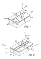
- a substrate 12 of high quality optical material such as an x-cut or y-cut crystalline birefringent material, has a localized region of increased refractive index to define a waveguide 14 along the z-axis.
- the waveguide 14 can be formed by a number of processes, one of which is the in-diffusion of a transition metal, such as titanium. Electric potential is applied to the waveguide device 10 by leads 16 and 18 connected to electrodes 20 and 22, respectively, in the form of thin strips of metal deposited on or near the waveguide 14.
- a thin layer 24 of high quality dielectric material for example, about 0.1 micron of silicon dioxide, has ordinarily been provided by sputter deposition on the substrate 12 between the waveguide 14 and the electrodes 20 and 22.
- planar waveguide devices In planar waveguide devices according to the present invention, an exemplary example of which is a mode conversion device, identified generally by the reference numeral 11 in Fig. 2, a planar substrate 13 made of a crystalline birefringent material, such as lithium niobate (LiNbO3) or lithium tantalate (LiTaO3), is cut in the x-or y-crystalline directions and has a waveguide 15 formed within acceptable limits substantially parallel to the z-axis.
- a planar substrate 13 made of a crystalline birefringent material, such as lithium niobate (LiNbO3) or lithium tantalate (LiTaO3)
- a magnesium oxide buffer layer 17 that overlies it, including waveguide 15, throughout its width.
- a magnesium oxide buffer layer 17 On top of the buffer layer 17 are deposited three metallic electrodes, 19, 21 and 23 having leads 25, 27 and 29, respectively. Electrode 23 sits directly over waveguide 15, and electrodes 19 and 21 sit with their inboard edges adjacent the outboard edges of waveguide 15.
- the channel waveguide 15 is formed by the indiffusion of a thin Ti stripe which is oriented parallel to the substrate z-axis.
- TE and TM modes propagate with very nearly the same effective indices when both are well guided. This is the case since the Ti dopant increases the ordinary index of the material to faciltiate guiding for TE as well as TM modes.
- Mode conversion is realized by placing the pair of electrodes, 19 and 21, parallel to and on either side of the channel waveguide 15, as well as the third electrode 23 directly on top of it.
- the effective indices of orthogonally polarized TE and TM modes are forced to near equality by action of the r(12) and r(22) electrooptic coefficients.
- electrode set 1 must sustain a bias voltage. In many instances, it would be impractical to apply such D.C. bias fields since they may lead to degradation of mode conversion behavior as well as time dependent drift in the characteristics of the device. Here, these effects are minimized by burying the waveguide and symmetrizing its axial index distribution.
- the technique used in this embodiment to depress the index of the channel waveguide surface to symmetrize the index distribution involves diffusion of a thin layer of magnesium oxide into the surface of the substrate following waveguide formation.
- the magnesium dopant acts as an index depressing agent and thereby cancels the effect of the titanium in raising the index of the guide surface.
- Waveguides were formed in this geometry by diffusing into the substrate 400 A thick Ti stripes 3 microns in width at 1100°C for 5 hours. Following this initial diffusion, the substrate was coated with 230 A of Mg and returned to the furnace and oxidized at 900°C for 4 hours in flowing wet oxygen.
- the resulting guide supported a single mode at a wavelength of .632 microns.
- the three-electrode pattern was subsequently placed over the buried channel.
- the center electrode was 5 microns in width and the gaps between center and outer electrodes was 5 microns. Electrodes were 12 mm in length.
- the devices were tested for relative attenuation of the TE and TM modes prior to applying bias fields. No preferential loss in the TM mode was observed.
- the guide was excited with TM polarized light and a bias of 14 volts was applied to the outer electrodes, 19 and 21. A 30 volt (pp) A.C. signal was applied to the center electrode. The throughput characteristic of the TE and TM modes were separately monitored.
- Electrodes 36 and 38 are defined by thin strips of metal to which leads 40 and 42, respectively, are attached and are positioned on or near the waveguide 34.
- a buffer layer 44 is provided directly in the substrate 32 to isolate the waveguide 34 from the metallic electrodes 36 and 38.
- the waveguide 34 is formed as a localized region of raised index of refraction in the shape of a channel by the in-diffusion of titanium or other transition metal in connection with appropriate masking of the substrate 32 to define an intermediate product, as can be seen from Fig. 3.
- the substrate 32 and its waveguide 34, having a raised index of refraction relative to the rest of the substrate, are subjected to a proton exchange, which, for the x-cut or y-cut material having the waveguide 34 substantially parallel to the z-axis, actually lowers the oridnary index of refraction of the material in a stratum at the surface.
- the stratum of reduced ordinary index of refraction defines the buffer layer 44 between the waveguide 34 and the metallic electrodes 36 and 38, which are later deposited on the buffer layer 44.
- the lowered ordinary index is effective in isolating the electromagnetic waves in the waveguide 34 from the electrodes 36 and 38 because both the TE and TM modes "see", that is, they are influenced by, the ordinary index of refraction in the crystalline birefringent material.
- the ion exchange, or proton exchange, takes place by immersing the substrate 32 in a bath of melted benzoic acid, for example, at 250°C for three minutes to deplete the lithium from a stratum approximately 0.3 microns thick at the surface and thereby form the buffer layer 44, as can be seen from Fig. 5.
- the ordinary index of refraction of portions 44a of the buffer layer 44 lying in the substrate 32 but outside the region exposed to the titanium in-diffusion is reduced below the ordinary index of the rest of the substrate by approximately 0.02.
- the burying of the waveguide 34 is believed to help make the modal power distribution of the waves more symmetrical with respect to the axis of the waveguide 34 and, thereby, improve the efficiency of coupling between the waveguide and optical fibers. It is also believed that the proton exchange process increases the electrical conductivity of the surface of the waveguide 34, thereby making it easier for the ionized impurities in the substrate to migrate until neutralized and avoiding the perturbations of the visible wavelengths by charge accumulation near the waveguide.
Landscapes
- Physics & Mathematics (AREA)
- Nonlinear Science (AREA)
- Chemical & Material Sciences (AREA)
- Engineering & Computer Science (AREA)
- Ceramic Engineering (AREA)
- Crystallography & Structural Chemistry (AREA)
- General Physics & Mathematics (AREA)
- Optics & Photonics (AREA)
- Optical Integrated Circuits (AREA)
Applications Claiming Priority (2)
| Application Number | Priority Date | Filing Date | Title |
|---|---|---|---|
| US06/906,931 US4775208A (en) | 1986-06-06 | 1986-09-15 | Planar waveguide mode converter device |
| US906931 | 1986-09-15 |
Publications (3)
| Publication Number | Publication Date |
|---|---|
| EP0260416A2 true EP0260416A2 (de) | 1988-03-23 |
| EP0260416A3 EP0260416A3 (en) | 1988-12-14 |
| EP0260416B1 EP0260416B1 (de) | 1993-04-28 |
Family
ID=25423244
Family Applications (1)
| Application Number | Title | Priority Date | Filing Date |
|---|---|---|---|
| EP87110998A Expired - Lifetime EP0260416B1 (de) | 1986-09-15 | 1987-07-29 | Planare Wellenleitervorrichtung |
Country Status (5)
| Country | Link |
|---|---|
| US (1) | US4775208A (de) |
| EP (1) | EP0260416B1 (de) |
| JP (1) | JPH083581B2 (de) |
| CA (1) | CA1298390C (de) |
| DE (2) | DE3785630T2 (de) |
Cited By (1)
| Publication number | Priority date | Publication date | Assignee | Title |
|---|---|---|---|---|
| GB2271192A (en) * | 1992-09-01 | 1994-04-06 | Ericsson Telefon Ab L M | Optical switch |
Families Citing this family (17)
| Publication number | Priority date | Publication date | Assignee | Title |
|---|---|---|---|---|
| DE3874199T2 (de) * | 1987-05-01 | 1993-02-11 | Nippon Electric Co | Einrichtung zur polarisationssteuerung. |
| FR2615006B1 (fr) * | 1987-05-04 | 1991-10-04 | Thomson Csf | Guide d'onde optique integre, son procede de fabrication, et son utilisation dans un modulateur electro-optique |
| JPS6457207A (en) * | 1987-08-28 | 1989-03-03 | Hitachi Ltd | Waveguide type optical device |
| US4984861A (en) * | 1989-03-27 | 1991-01-15 | United Technologies Corporation | Low-loss proton exchanged waveguides for active integrated optic devices and method of making same |
| US5020872A (en) * | 1990-01-04 | 1991-06-04 | Smiths Industries Aerospace & Defense Systems Incorporated | Method of operating an electrooptic modulator |
| US5359682A (en) * | 1990-03-07 | 1994-10-25 | Cselt-Centro Studi E Laboratori Telecomunicazioni S.P.A. | Method of adjusting the operation characteristics of integrated optical devices |
| IT1240124B (it) * | 1990-03-07 | 1993-11-27 | Cselt Centro Studi Lab Telecom | Metodo per ritoccare le caratteristiche di funzionamento di dispositivi ottici integrati. |
| IT1245961B (it) * | 1991-05-10 | 1994-11-07 | Alenia Aeritalia & Selenia | Processo di fabbricazione di guide ottiche a canale in linbo3. |
| EP0620458A4 (de) * | 1992-09-07 | 1995-02-01 | Nippon Kogaku Kk | Optisches wellenleiterbauelement und ein dieses verwendendes optisches instrument. |
| JPH06235833A (ja) * | 1993-02-09 | 1994-08-23 | Nikon Corp | 光導波路 |
| DE69415286T2 (de) * | 1993-11-25 | 1999-05-06 | Northern Telecom Ltd., Montreal, Quebec | Polarisationwandler |
| JP3771287B2 (ja) * | 1994-04-15 | 2006-04-26 | 富士写真フイルム株式会社 | 導波路型電気光学素子 |
| US5834055A (en) * | 1995-08-30 | 1998-11-10 | Ramar Corporation | Guided wave device and method of fabrication thereof |
| US5749132A (en) * | 1995-08-30 | 1998-05-12 | Ramar Corporation | Method of fabrication an optical waveguide |
| JP2850950B2 (ja) * | 1996-01-19 | 1999-01-27 | 日本電気株式会社 | 導波型光デバイス |
| JP3425843B2 (ja) * | 1996-09-30 | 2003-07-14 | 富士写真フイルム株式会社 | 光導波路素子の電極の形成方法 |
| AUPO405696A0 (en) | 1996-12-06 | 1997-01-09 | Ici Australia Operations Proprietary Limited | Herbicidal compositions |
Family Cites Families (23)
| Publication number | Priority date | Publication date | Assignee | Title |
|---|---|---|---|---|
| JPS5038342B2 (de) * | 1971-12-01 | 1975-12-09 | ||
| US3837827A (en) * | 1973-01-18 | 1974-09-24 | Bell Telephone Labor Inc | Method for producing optical waveguiding layers in solid transparent media |
| US4220395A (en) * | 1974-05-13 | 1980-09-02 | Regents Of University Of California | Polarization converter and circuit elements for use in optical waveguides |
| US3923376A (en) * | 1974-08-02 | 1975-12-02 | Us Navy | Electro-optic waveguide beam deflector |
| JPS6032843B2 (ja) * | 1976-12-17 | 1985-07-30 | 日本電気株式会社 | タンタル酸リシウム光導波路の形成方法 |
| JPS5392149A (en) * | 1977-01-24 | 1978-08-12 | Mitsubishi Electric Corp | Method of fabricating thin film light wave guide |
| FR2399736A1 (fr) * | 1977-08-05 | 1979-03-02 | Thomson Csf | Procede de fabrication d'une structure electro-optique comportant une electrode integree et composant optoelectronique utilisant ladite structure |
| JPS5435781A (en) * | 1977-08-25 | 1979-03-16 | Sony Corp | Timer device |
| US4400052A (en) * | 1981-03-19 | 1983-08-23 | Bell Telephone Laboratories, Incorporated | Method for manufacturing birefringent integrated optics devices |
| JPS57158616A (en) * | 1981-03-25 | 1982-09-30 | Ricoh Co Ltd | Optical coupler |
| US4645293A (en) * | 1981-03-25 | 1987-02-24 | Taizo Yoshida | Optical waveguide coupler having a grating electrode |
| JPS58172619A (ja) * | 1982-04-01 | 1983-10-11 | Matsushita Electric Ind Co Ltd | 光デバイス用基板 |
| FR2533714A1 (fr) * | 1982-09-28 | 1984-03-30 | Thomson Csf | Dispositif coupleur optique integre non lineaire et oscillateur parametrique comprenant un tel dispositif |
| JPS59181317A (ja) * | 1983-03-31 | 1984-10-15 | Sumitomo Electric Ind Ltd | 光変調素子 |
| US4533207A (en) * | 1983-06-21 | 1985-08-06 | At&T Bell Laboratories | Wavelength tunable TE to TM mode converter |
| US4691983A (en) * | 1983-10-14 | 1987-09-08 | Hitachi, Ltd. | Optical waveguide and method for making the same |
| JPS60162207A (ja) * | 1984-02-01 | 1985-08-24 | Hitachi Ltd | 光導波路およびその製造方法 |
| US4711515A (en) * | 1984-05-29 | 1987-12-08 | American Telephone And Telegraph Company, At&T Bell Laboratories | Electrooptic polarization multiplexer/demultiplexer |
| US4607909A (en) * | 1984-06-14 | 1986-08-26 | Polaroid Corporation | Method for modulating a carrier wave |
| US4547262A (en) * | 1984-08-30 | 1985-10-15 | Sperry Corporation | Method for forming thin film passive light waveguide circuit |
| US4697868A (en) * | 1985-08-12 | 1987-10-06 | Trw Inc. | Integrated optical waveguide polarizer |
| US4691984A (en) * | 1985-09-26 | 1987-09-08 | Trw Inc. | Wavelength-independent polarization converter |
| US4714312A (en) * | 1986-05-19 | 1987-12-22 | Trw Inc. | Electrostatically biased electrooptical devices |
-
1986
- 1986-09-15 US US06/906,931 patent/US4775208A/en not_active Expired - Lifetime
-
1987
- 1987-07-29 DE DE8787110998T patent/DE3785630T2/de not_active Expired - Fee Related
- 1987-07-29 DE DE198787110998T patent/DE260416T1/de active Pending
- 1987-07-29 CA CA000543215A patent/CA1298390C/en not_active Expired - Fee Related
- 1987-07-29 EP EP87110998A patent/EP0260416B1/de not_active Expired - Lifetime
- 1987-08-27 JP JP62211542A patent/JPH083581B2/ja not_active Expired - Fee Related
Non-Patent Citations (4)
| Title |
|---|
| APPLIED PHYSICS LETTERS, vol. 25, no. 8, 15th October 1974, pages 458-460, American Institute of Physics; R.V. SCHMIDT et al.: "Metal-diffused optical waveguides in LiNbO3", * |
| JOURNAL OF APPLIED PHYSICS, vol. 49, no. 6, June 1978, page 3150-3154; American Institute of Physics; J. NODA et al.: "Effect of Mg diffusion on Ti-diffused LiNbO3 waveguides", * |
| OPTICS COMMUNICATIONS, vol. 42, no. 2, 15th June 1982, pages 101-103; M. DE MICHELI et al.: "Fabrication and characterization of titanium indiffused proton exchanged (tipe) waveguides in lithium niobate", * |
| OPTICS LETTERS, vol. 11, no. 1, January 1986, pages 39-41, Optical Society of America, New York, US; S. THANIYAVARN: "Wavelength-independent, optical-damage-immune liNbO3 TE-TM mode converter", * |
Cited By (2)
| Publication number | Priority date | Publication date | Assignee | Title |
|---|---|---|---|---|
| GB2271192A (en) * | 1992-09-01 | 1994-04-06 | Ericsson Telefon Ab L M | Optical switch |
| GB2271192B (en) * | 1992-09-01 | 1996-10-09 | Ericsson Telefon Ab L M | Near Z digital switch |
Also Published As
| Publication number | Publication date |
|---|---|
| CA1298390C (en) | 1992-03-31 |
| DE260416T1 (de) | 1988-07-21 |
| JPH083581B2 (ja) | 1996-01-17 |
| US4775208A (en) | 1988-10-04 |
| EP0260416B1 (de) | 1993-04-28 |
| JPS6375725A (ja) | 1988-04-06 |
| EP0260416A3 (en) | 1988-12-14 |
| DE3785630D1 (de) | 1993-06-03 |
| DE3785630T2 (de) | 1993-08-05 |
Similar Documents
| Publication | Publication Date | Title |
|---|---|---|
| EP0260416A2 (de) | Planare Wellenleitervorrichtung | |
| CN100410732C (zh) | 光调制器 | |
| Meier et al. | Integrated optical E-field probes with segmented modulator electrodes | |
| EP0149678A1 (de) | Integrierte optische schaltung | |
| WO1999012062A1 (en) | Integrated optical polariser | |
| US4983006A (en) | Polarization-independent optical waveguide switch | |
| EP0554593B1 (de) | Verfahren zur Herstellung einer Vorrichtung, die ein Substrat mit pyroelektrischem Effekt benutzt | |
| US12204185B2 (en) | Optical waveguide element and optical modulator | |
| US3923373A (en) | Coupling to graded index waveguide | |
| EP0188889A2 (de) | Lichtmodulator mit einer optischen Faser | |
| JP2873203B2 (ja) | 導波路型光デバイス | |
| CA1226930A (en) | Method for modulating a carrier wave | |
| JP2655678B2 (ja) | 集積光導波路とその製造方法、および集積光導波路を用いた電気光学変調器 | |
| US4948407A (en) | Proton exchange method of forming waveguides in LiNbO3 | |
| EP1752817A1 (de) | Optische wellenleitereinrichtung | |
| JPH07120631A (ja) | 光導波路型部品 | |
| JPH0829745A (ja) | 光導波路デバイス | |
| US20220221744A1 (en) | Integrated compact z-cut lithium niobate modulator | |
| EP0178815B1 (de) | Optische Wellenleiter | |
| Majd et al. | Low-loss Ti: LiNbO/sub 3/-waveguide bends prepared by MgO indiffusion | |
| JP3195033B2 (ja) | 光導波路およびその形成方法 | |
| JP3050202B2 (ja) | 光導波路デバイスおよびその製造方法 | |
| JPH02114243A (ja) | 光制御デバイス及びその製造方法 | |
| Heibei et al. | Strip waveguides in LiNbO 3 fabricated by combined metal diffusion and ion implantation | |
| KR100374345B1 (ko) | 매립형광도파로제작방법 |
Legal Events
| Date | Code | Title | Description |
|---|---|---|---|
| PUAI | Public reference made under article 153(3) epc to a published international application that has entered the european phase |
Free format text: ORIGINAL CODE: 0009012 |
|
| AK | Designated contracting states |
Kind code of ref document: A2 Designated state(s): DE FR GB NL |
|
| TCNL | Nl: translation of patent claims filed | ||
| EL | Fr: translation of claims filed | ||
| DET | De: translation of patent claims | ||
| PUAL | Search report despatched |
Free format text: ORIGINAL CODE: 0009013 |
|
| AK | Designated contracting states |
Kind code of ref document: A3 Designated state(s): DE FR GB NL |
|
| 17P | Request for examination filed |
Effective date: 19890608 |
|
| 17Q | First examination report despatched |
Effective date: 19911021 |
|
| GRAA | (expected) grant |
Free format text: ORIGINAL CODE: 0009210 |
|
| AK | Designated contracting states |
Kind code of ref document: B1 Designated state(s): DE FR GB NL |
|
| REF | Corresponds to: |
Ref document number: 3785630 Country of ref document: DE Date of ref document: 19930603 |
|
| ET | Fr: translation filed | ||
| PLBE | No opposition filed within time limit |
Free format text: ORIGINAL CODE: 0009261 |
|
| STAA | Information on the status of an ep patent application or granted ep patent |
Free format text: STATUS: NO OPPOSITION FILED WITHIN TIME LIMIT |
|
| 26N | No opposition filed | ||
| REG | Reference to a national code |
Ref country code: GB Ref legal event code: IF02 |
|
| PGFP | Annual fee paid to national office [announced via postgrant information from national office to epo] |
Ref country code: FR Payment date: 20030609 Year of fee payment: 17 |
|
| PGFP | Annual fee paid to national office [announced via postgrant information from national office to epo] |
Ref country code: GB Payment date: 20030612 Year of fee payment: 17 |
|
| PGFP | Annual fee paid to national office [announced via postgrant information from national office to epo] |
Ref country code: NL Payment date: 20030619 Year of fee payment: 17 |
|
| PGFP | Annual fee paid to national office [announced via postgrant information from national office to epo] |
Ref country code: DE Payment date: 20030625 Year of fee payment: 17 |
|
| PG25 | Lapsed in a contracting state [announced via postgrant information from national office to epo] |
Ref country code: GB Free format text: LAPSE BECAUSE OF NON-PAYMENT OF DUE FEES Effective date: 20040729 |
|
| PG25 | Lapsed in a contracting state [announced via postgrant information from national office to epo] |
Ref country code: NL Free format text: LAPSE BECAUSE OF NON-PAYMENT OF DUE FEES Effective date: 20050201 Ref country code: DE Free format text: LAPSE BECAUSE OF NON-PAYMENT OF DUE FEES Effective date: 20050201 |
|
| GBPC | Gb: european patent ceased through non-payment of renewal fee |
Effective date: 20040729 |
|
| PG25 | Lapsed in a contracting state [announced via postgrant information from national office to epo] |
Ref country code: FR Free format text: LAPSE BECAUSE OF NON-PAYMENT OF DUE FEES Effective date: 20050331 |
|
| NLV4 | Nl: lapsed or anulled due to non-payment of the annual fee |
Effective date: 20050201 |
|
| REG | Reference to a national code |
Ref country code: FR Ref legal event code: ST |
|
| REG | Reference to a national code |
Ref country code: GB Ref legal event code: 732E |
|
| REG | Reference to a national code |
Ref country code: FR Ref legal event code: TP Ref country code: FR Ref legal event code: CD Ref country code: FR Ref legal event code: CA |