EP0258947A2 - Videomonitor-Schnittstelle für digitale Farbsignale - Google Patents
Videomonitor-Schnittstelle für digitale Farbsignale Download PDFInfo
- Publication number
- EP0258947A2 EP0258947A2 EP87201647A EP87201647A EP0258947A2 EP 0258947 A2 EP0258947 A2 EP 0258947A2 EP 87201647 A EP87201647 A EP 87201647A EP 87201647 A EP87201647 A EP 87201647A EP 0258947 A2 EP0258947 A2 EP 0258947A2
- Authority
- EP
- European Patent Office
- Prior art keywords
- digital
- color
- signal
- signals
- analog
- Prior art date
- Legal status (The legal status is an assumption and is not a legal conclusion. Google has not performed a legal analysis and makes no representation as to the accuracy of the status listed.)
- Withdrawn
Links
- 239000003086 colorant Substances 0.000 claims abstract description 35
- 230000000875 corresponding effect Effects 0.000 claims abstract description 31
- 230000015654 memory Effects 0.000 claims abstract description 21
- 230000001276 controlling effect Effects 0.000 claims abstract description 4
- 230000004044 response Effects 0.000 claims description 9
- 230000000694 effects Effects 0.000 claims description 3
- 235000019642 color hue Nutrition 0.000 description 2
- 239000002131 composite material Substances 0.000 description 2
- 238000006243 chemical reaction Methods 0.000 description 1
- 230000006870 function Effects 0.000 description 1
- 238000012986 modification Methods 0.000 description 1
- 230000004048 modification Effects 0.000 description 1
- 238000012544 monitoring process Methods 0.000 description 1
- 229920006395 saturated elastomer Polymers 0.000 description 1
- 230000000007 visual effect Effects 0.000 description 1
Images


Classifications
-
- H—ELECTRICITY
- H04—ELECTRIC COMMUNICATION TECHNIQUE
- H04N—PICTORIAL COMMUNICATION, e.g. TELEVISION
- H04N5/00—Details of television systems
- H04N5/222—Studio circuitry; Studio devices; Studio equipment
- H04N5/262—Studio circuits, e.g. for mixing, switching-over, change of character of image, other special effects ; Cameras specially adapted for the electronic generation of special effects
- H04N5/268—Signal distribution or switching
-
- G—PHYSICS
- G09—EDUCATION; CRYPTOGRAPHY; DISPLAY; ADVERTISING; SEALS
- G09G—ARRANGEMENTS OR CIRCUITS FOR CONTROL OF INDICATING DEVICES USING STATIC MEANS TO PRESENT VARIABLE INFORMATION
- G09G1/00—Control arrangements or circuits, of interest only in connection with cathode-ray tube indicators; General aspects or details, e.g. selection emphasis on particular characters, dashed line or dotted line generation; Preprocessing of data
- G09G1/28—Control arrangements or circuits, of interest only in connection with cathode-ray tube indicators; General aspects or details, e.g. selection emphasis on particular characters, dashed line or dotted line generation; Preprocessing of data using colour tubes
- G09G1/285—Interfacing with colour displays, e.g. TV receiver
Definitions
- This invention relates to a colour interface circuit for a video monitor which produces color images in response to signals supplied by a digital processor, and particularly to such an interface circuit which enables a monitor operating in a standard format of primary color analog input signals, such as red, green and blue, to display colors signified by digital signals which are in various other colour formats.
- Information produced by a digital processor is commonly displayed on the screen of a color CRT to permit visual monitoring of such information.
- the input terminals of the CRT monitor require signals which control the relative intensities of each of a set of three primary colors on the monitor screen, the standard set or format of primary colors being red, green and blue.
- An intensity (“I") signals is also frequently added to the color signals to control their relatively purity with respect to a reference gray level. Since the processor produces digital output signals, digital-to-analog conversion is required to obtain corresponding analog signals for application to the monitor input terminals. This is one of the functions of a display interface circuit between the processor and the monitor.
- processors for example the type 5150 (RGBI) of IBM Corporation, produce digital signals respective bits of which, with few exceptions, respectively correspond to the individual R, G, B primary colors of the standard video monitor color format.
- processors such as the type IIe (XRGB) of Apple Computer Corporation, produce digital signals which completely depart from the standard primary color format and are intended for a monitor specifically adapted to operate in the format of that particular processor.
- respective bits of the digital signal identify colors which are actually combinations of different proportions of the standard R, G and B primary colors. Consequently, it has not been possible to employ the same monitor for such processors as well as for processors operating in the standard B, G and R color format.
- Suppliers of different kinds of digital processors have therefore had to maintain an inventory almost an equal number of matching display monitors, and purchasers of particular processors have been limited in the choice of monitors available to them.
- the invention provides a color interface circuit for translating digital signals signifying colors in any of various color formats into analog signals for controlling respective primary colors of a video monitor displaying colors in a standard color format, whereby the colors displayed by the monitor match the colors signified by the digital signals.
- the interface For translation from either of two color formats, the interface requires only a single control line in order to switch from translation of digital signals corresponding to one of such formats to translation of digital signals corresponding to the other of such formats.
- Translation of more than two formats would of course require a sufficient number of control lines to identify them; e.g., two control lines (in addition to the four color address lines) would permit translation of up to four formats
- a color interface circuit in accordance with the invention comprises digital memory means which stores therein a plurality of digital words respectively corresponding to each of the colors signified by respective digital color signals, each such digital word having a predetermined number of bits, such memory means reading-out the digital word corresponding to any digital color signal upon receiving such signal.
- the circuit further comprises a plurality of word bit combining networks which respectively produce analog color signals corresponding to weighted summations of the bits of a digital word applied thereto, such analog signals respectively corresponding to the respective primary colors of the video monitor, such combining networks being connected to the memory means to receive the bits of a digital word read-out therefrom in response to a received digital color signal.
- the combining networks weight the bits of a digital word applied thereto so that the relative proportions of the weighted analog summations thereof are the same as the relative proportions of the primary colors of the video monitor for displaying a color matching the color signified by the digital color signal.
- the interface circuit comprises switching means for altering the digital value of a control bit included in each of the digital words stored in the digital memory means, whereby the digital word supplied to the combining networks can be altered in correspondence with the color format of the received digital color signals.
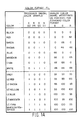
- the first two columns thereof show the colors corresponding to all possible digital color signals produced by a typical digital processor such as the IBM Corporation type 5150 (RGBI).
- RGBI IBM Corporation type 5150
- Each signal comprises four bits generically identified by their binary order 1, 2, 4 or 8, from the least to the most significant bit.
- R, G, B and I signals the I signal controlling the gray level of the displayed color. Since there are sixteen possible combinations of four bits, there are sixteen possible colors corresponding thereto.
- This color format will be referred to hereinafter as color format F1.
- the B, G and R digital signals are intended for respective input terminals of a color display monitor associated with the processor, the I signal being applied in common to all terminals to establish a gray intensity level on the monitor screen.
- the I signal is a "1” the displayed colors are less saturated, or lighter, then when it is "0".
- the R, G and B digital signals of this processor respectively correspond to the R, G and B analog signal inputs of a video monitor operating in the standard R, G and B color format. That is, a "1" level of the digital "R” signal signifies the same analog signal level at the R input terminal for every color to which such digital R signal contributes, and similarly for the B and G digital signals.
- the analog G signal corresponding to a "1" digital G signal must be reduced by approximately 30% from the level which a "1" digital G signal signifies for any other color to which the digital G signal contributes.
- Applicant has also found that to duplicate the effect of the digital I signal on any composite displayed color the intensity levels of each of the analog primary color signals contributing to such composite color must be increased by 33% with respect to their zero reference level.
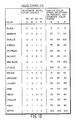
- a digital color signal format which totally departs from the standard R, G and B format is shown by the table in Fig. 1B, which is applicable to the Apple Computer Corporation IIe (XRGB) digital processor. This is referred to hereafter as color format F2.
- color format F2 As seen in the first two columns of the table, the four bits of each digital signal from the processor have for convenience of identification been denoted I, B, G and R.
- the sixteen possible monitor display colors signified by these signals are altogether different from those signified by the digital color signals in the format of Fig. 1A and from those of digital signals in the standard R, G, B color format.
- the I signal contributes to half of all the sixteen colors, as it also does in Fig.
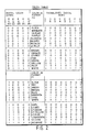
- An interface circuit for translating digital color signals in either the F1 or F2 color format into analog color signals in the standard format must first translate each of the 32 possible digital signals into digital words which identify the relative weightings of such analog color signals so as to result in thesame colors on the video monitor as those represented by the input digital words. Since different combinations of 10 analog weighting elements are sufficient to supply the necessary number of weighting factors, translation to digital words comprising 10 bits could be employed. However, since standard digital integrated circuits are designed for processing digital words which are in multiples of 8 bits, it is preferably to translate to 8 bit digital words and to derive 2 additional bits directly from the input digital color signals. This is described in more detail hereinafter.
- Translation to 8 bit digital words may be effected in accordance with the truth table shown in Fig. 2,wherein the inputs represent digital color signals in either of the primary color formats F1 and F2.
- the B, G, R and I bits have been supplemented by a fifth control bit C which identifies the particular primary color format to which the color signals relate; e.g. a "0" for color format F1 and a "1" for color format F2.
- the resulting 32 sets of five bits, designated A0-A4 may serve as the addresses of 32 locations in digital memory means, such as a programmable read-only memory (PROM), each such location storing an 8-bit word.
- PROM programmable read-only memory
- the respective bits of such words constitute the inputs to an analog weighting network, such as described hereinafter, which derive weighted summations thereof signifying the relative proportions of B, G and R analog color signals in the standard color format so as to cause the video monitor to produce colors matching those signified by the corresponding digital input signals.
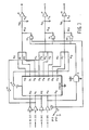
- Fig. 3 an interface circuit in accordance with the foregoing description. It comprises a digital memory 1 which may be a PROM such as the type 82S123 manufactured by Signetics Corporation and having five inputs A0-A4 and eight outputs D0-D7. Conventional ROMS, EPROMS and other kinds of memories could also be exployed. Memory 1 is conventionally powered so that a "1" bit is, for example, at a fixed potential and a "0" bit is at ground potential. If the power supply provides +5V, a "1" bit will be at that potential. The R, G, B and I bits of the digital color signals are respectively applied to inputs A0-A3.
- PROM such as the type 82S123 manufactured by Signetics Corporation and having five inputs A0-A4 and eight outputs D0-D7.
- Conventional ROMS, EPROMS and other kinds of memories could also be exployed.
- Memory 1 is conventionally powered so that a "1" bit is, for example, at a fixed potential
- the control bit C is provided by applying either ground or a +5V supply potential via a resistor to input terminal A4, a switch 2 being operable to selectively connect or disconnect terminal A4 to or from ground.
- operation of switch 2 sets the C bit to "0" and when not operated the C bit at terminal A4 is "1".
- the eight bits of the translated digital word corresponding to each input digital signal are produced at outputs D0-D7 of PROM 1, in accordance with a truth table in Fig. 2.
- Outputs D0-D2 are respectively connected by three attenuating elements such as resistors R0-R2 to a summing terminal S R which is returned to ground by an attenuating element such as a resistor R10. Resistors R0-R2 are proportioned to established the requisite analog weighting factors for deriving the analog R color signal produced by the translator.
- Outputs D3-D5 of PROM 1 are respectively connected by attenuating elements such as resistors R3-R5 to a summing terminal S G which is returned to ground by an attenuating element such as a resistor R11. Resistors R3-R5 are proportioned to establish the requisite analog weighting factors for deriving the analog G color output signal produced by the translator.
- Outputs D6 and D7 are respectively connected by attenuating elements such as resistors R6 and R7 to a summing terminal S B which is returned to ground by an attenuating element such as a resistor R12 and are proportioned to establish the requisite analog weighting factors for deriving the analog B color signal produced by the translator.
- the analog G signal requires 11 different weighting levels, which can be provided by least 4 attenuating elements. Accordingly, besides being utilized for color translation by PROM 1, the input digital signal G bit at input terminal A1 is also routed around PROM 1 and supplied through a buffer amplifier 4 and another attenuating element such as a resistor R8 directly to G summing terminal S G . Similarly, since the B analog signal requires 7 weighting levels, besides being utilized for color translation by PROM 1 and B bit of the digital signal at input terminal A2 is further routed around PROM 1 and supplied through a buffer amplifier 5 and an attenuating element such as a resistor R9 directly to B summing terminal S B . Resistors R8 and R9 are respectively proportioned relative to the other analog weighting resistors connected to terminals S G and S B , respectively, to establish the further analog weighting factors required for those signals as shown in Figs. 1A and 1B.
- Summing terminals S R , S G and S B are respectively connected to ground reference potential by resistors R10, R11, R12, and these are selected to have relatively low attenuation or resistance relative to each of the analog signal weighting resistors connected to the summing terminals. The voltages at those terminals will therefore respectively be proportional to the sum of the reciprocals of the resistances of the weighting resistors connected thereto.
- the analog summation voltages so produced at summing terminals S R , S G and S B are applied to the inputs of respective buffer amplifiers 6, 7 and 8 connected thereto, such as emitter follower transistor amplifiers, in order to obtain reduced output impedance.
- the output signals from amplifiers 6, 7 and 8 thereby constitute R, G and B analog signals for application to a video monitor CRT operating in the standard color format.
- the I bit of each digital signal affects the gray or luminence level of each of the analog color signals as well as the color hues corresponding thereto.
- the I bit only affects the color hues of the analog color signals.
- the I bit of the input digital color signal is also applied via an inverter 9 to an input of each of three NAND gates 10, 11, 12, the outputs of which are respectively connected by analog weighting elements such as resistors R13, R14, R15 to the respective analog summing terminals S R , S G and S B .
- the signal attenuation or resistance of these resistors is set in such proportions relative to the other analog summing resistors connected to the corresponding running terminals to provide I signal weighting factors in accordance with color format F1 as shown in Fig. 1A.
- the control bit C besides setting PROM 1 for color translation in accordance with either of color formats F1 and F2, is also utilized to gate the I signal. For that purpose, control bit C is applied to a second input of eachof NAND gates 10, 11 and 12.
- control signal C is a "1"
- a "1" I bit will be inverted into a "0" by inverter 9 and applied to each of NAND gates 10, 11 and 12.
- Fig. 3 The operation of the color interface circuit in Fig. 3 will be explained by two examples: translation of light blue in color format F2, and of brown in color format F1. These examples are respectively illustrated in Figs. 4 and 5, wherein the block 10 labeled "decode logic" represents the portion of the complete interface circuit of Fig. 3 comprising PROM 1 and the interconnections of the G and B inputs thereto to the G auxiliary summing resistor R8 and the B auxiliary summing resistor R9.
- Light blue in color format F2 is signified by a digital input signal 11100. Accordingly, these are the input digital signal bits in Fig. 4.
- Devode logic block 10 translates that digital signal to a digital word as shown in Fig. 2, which results in +5V on the outputs of logic block 10 corresponding to the "1" bits in the translated digital word. The remaining "0" outputs will be at ground potential.
- the analog voltage corresponding to summation of these digital voltages, weighted in proportion to the reciprocals of the resistance of the weighting resistors connected to these outputs, will be produced at terminals S R , S G and S B .
- These weighting proportions are set in accordance with the weighting factors shown in Figs. 1A and 1B.
- a suitable set of relative resistance of the various weighting resistors, and the corresponding inverse values of conductances thereof is as follows:
- the summed output voltage at any summing terminal is proportional to the sum of the conductances connected thereto. Accordingly, the maximum voltages at terminals S R , S G and S B will be respectively proportional to 1.60, 1.323 and 1.57
- Fig. 4 omits the resistors R13, R14, and R15 even though they are actually in the I signal bit paths connected to terminals S R , S G and S B as shown in Fig. 3. This is because, as explained above, when the control signal bit C is "0" the outputs of NAND gates 10, 11 and 12 remain at “1" regardless of the value of the digital I bit. Consequently, the presence of resistors R13, R14 and R15 does not alter the percentage changes in the magnitudes of the voltages at terminals S R , S G and S B in response to changes in the translated digital color signals.
- Fig. 5 illustrating production of the color brown in color format F1
- the digital input signal as shown by the Truth Table in Fig. 2 is 11001.
- the corresponding translated digital word in Fig. 2 results in digital signals at the outputs of decode logic block 10 as shown in Fig. 5, including the "1" G signal routed to resistor R8 connected to G summing terminal S G and the "0" B signal routed to resistor R9 connected to the B summing terminal S B .
- Fig. 5 also includes the resistors R13, R14 and R15 which, as shown in Fig.
- Typical resistances of resistors R13, R14 and R15 are 1.2 K Ohm, 3.4 kOhm and 1.2 kOhm.
Landscapes
- Engineering & Computer Science (AREA)
- Radar, Positioning & Navigation (AREA)
- Remote Sensing (AREA)
- Physics & Mathematics (AREA)
- Computer Hardware Design (AREA)
- General Physics & Mathematics (AREA)
- Theoretical Computer Science (AREA)
- Multimedia (AREA)
- Signal Processing (AREA)
- Processing Of Color Television Signals (AREA)
- Digital Computer Display Output (AREA)
- Color Television Systems (AREA)
Applications Claiming Priority (2)
| Application Number | Priority Date | Filing Date | Title |
|---|---|---|---|
| US06/903,006 US4774495A (en) | 1986-09-02 | 1986-09-02 | Video monitor interface circuit for digital color signals |
| US903006 | 1992-06-23 |
Publications (2)
| Publication Number | Publication Date |
|---|---|
| EP0258947A2 true EP0258947A2 (de) | 1988-03-09 |
| EP0258947A3 EP0258947A3 (de) | 1990-10-17 |
Family
ID=25416772
Family Applications (1)
| Application Number | Title | Priority Date | Filing Date |
|---|---|---|---|
| EP19870201647 Withdrawn EP0258947A3 (de) | 1986-09-02 | 1987-08-31 | Videomonitor-Schnittstelle für digitale Farbsignale |
Country Status (4)
| Country | Link |
|---|---|
| US (1) | US4774495A (de) |
| EP (1) | EP0258947A3 (de) |
| JP (1) | JPS63118189A (de) |
| KR (1) | KR880004687A (de) |
Families Citing this family (2)
| Publication number | Priority date | Publication date | Assignee | Title |
|---|---|---|---|---|
| US4920344A (en) * | 1985-03-11 | 1990-04-24 | Ncr Corporation | Digitally compensated multiplying digital to analog converter |
| US5313300A (en) * | 1992-08-10 | 1994-05-17 | Commodore Electronics Limited | Binary to unary decoder for a video digital to analog converter |
Family Cites Families (6)
| Publication number | Priority date | Publication date | Assignee | Title |
|---|---|---|---|---|
| US3744050A (en) * | 1970-11-23 | 1973-07-03 | Lear Siegler Inc | Apparatus for providing an analog output in response to a digital input |
| NL7807503A (nl) * | 1977-07-14 | 1979-01-16 | Indep Broadcasting Authority | Transmissie en/of registratie van digitale signalen. |
| US4590463A (en) * | 1980-09-29 | 1986-05-20 | Rca Corporation | Digital control of color in CRT display |
| US4386345A (en) * | 1981-09-22 | 1983-05-31 | Sperry Corporation | Color and brightness tracking in a cathode ray tube display system |
| US4547797A (en) * | 1982-10-12 | 1985-10-15 | Sperry Corporation | Apparatus for color tracking and brightness correction for multi-gun color cathode ray tube display |
| GB2167926A (en) * | 1984-11-26 | 1986-06-04 | Philips Nv | Colour signal generator for crt image display |
-
1986
- 1986-09-02 US US06/903,006 patent/US4774495A/en not_active Expired - Fee Related
-
1987
- 1987-08-31 KR KR870009553A patent/KR880004687A/ko not_active Withdrawn
- 1987-08-31 EP EP19870201647 patent/EP0258947A3/de not_active Withdrawn
- 1987-08-31 JP JP62215532A patent/JPS63118189A/ja active Pending
Also Published As
| Publication number | Publication date |
|---|---|
| KR880004687A (ko) | 1988-06-07 |
| US4774495A (en) | 1988-09-27 |
| JPS63118189A (ja) | 1988-05-23 |
| EP0258947A3 (de) | 1990-10-17 |
Similar Documents
| Publication | Publication Date | Title |
|---|---|---|
| EP0385449B1 (de) | Ansteuervorrichtung für farbige Flüssigkristallanzeigen | |
| US5757298A (en) | Method and apparatus for error compensation using a non-linear digital-to-analog converter | |
| US5398075A (en) | Analog chroma keying on color data | |
| US6674413B2 (en) | Display control apparatus | |
| EP0264921A2 (de) | Digital-Analog-Wandler | |
| JPH0290197A (ja) | デイザー装置 | |
| US4918634A (en) | Key input apparatus | |
| US4695826A (en) | High accuracy digital-to-analog converter having symmetrical current source switching | |
| US5442379A (en) | High speed RAMDAC with reconfigurable color palette | |
| US5638090A (en) | Window-dependent brightness/tint control for video digital-to-analog converters | |
| CN100454334C (zh) | 多等级单色图像显示方法及其相关装置 | |
| US4725833A (en) | Tone control device in monochromatic tone display apparatus | |
| EP0204821B1 (de) | Schaltungsanordnung zum umwandeln von digitale farbinformationen darstellenden signalen in analoge spannungspegelsignale | |
| GB2223149A (en) | Digital data display system | |
| EP0258947A2 (de) | Videomonitor-Schnittstelle für digitale Farbsignale | |
| JP3016016B2 (ja) | カラーlcd駆動装置 | |
| US4626835A (en) | RGBI digital video control system having intensity level control and overall image strength control | |
| JPH0769671B2 (ja) | ディジタル−アナログ変換装置 | |
| CA1298422C (en) | Monitor interface circuit | |
| KR19990077552A (ko) | 액정구동회로 | |
| US5854633A (en) | Method of and system for dynamically adjusting color rendering | |
| US6460065B1 (en) | Circuit and method for partial product bit shifting | |
| US4974070A (en) | Colorgraphic reproduction system | |
| EP0422296A1 (de) | Anzeigesystem mit direktem Farbmodus | |
| JP2680940B2 (ja) | D/a変換器 |
Legal Events
| Date | Code | Title | Description |
|---|---|---|---|
| PUAI | Public reference made under article 153(3) epc to a published international application that has entered the european phase |
Free format text: ORIGINAL CODE: 0009012 |
|
| AK | Designated contracting states |
Kind code of ref document: A2 Designated state(s): DE FR GB |
|
| PUAL | Search report despatched |
Free format text: ORIGINAL CODE: 0009013 |
|
| AK | Designated contracting states |
Kind code of ref document: A3 Designated state(s): DE FR GB |
|
| RAP1 | Party data changed (applicant data changed or rights of an application transferred) |
Owner name: NORTH AMERICAN PHILIPS CORPORATION |
|
| 17P | Request for examination filed |
Effective date: 19910411 |
|
| 17Q | First examination report despatched |
Effective date: 19920730 |
|
| STAA | Information on the status of an ep patent application or granted ep patent |
Free format text: STATUS: THE APPLICATION IS DEEMED TO BE WITHDRAWN |
|
| 18D | Application deemed to be withdrawn |
Effective date: 19921210 |
|
| RIN1 | Information on inventor provided before grant (corrected) |
Inventor name: WOLTER. DONALD BRUCE Inventor name: RAFTER, PATRICK MICHAEL |