US4774495A - Video monitor interface circuit for digital color signals - Google Patents

Video monitor interface circuit for digital color signals Download PDF

Info

Publication number
US4774495A
US4774495A US06/903,006 US90300686A US4774495A US 4774495 A US4774495 A US 4774495A US 90300686 A US90300686 A US 90300686A US 4774495 A US4774495 A US 4774495A
Authority
US
United States
Prior art keywords
digital
color
signal
signals
analog
Prior art date
Legal status (The legal status is an assumption and is not a legal conclusion. Google has not performed a legal analysis and makes no representation as to the accuracy of the status listed.)
Expired - Fee Related
Application number
US06/903,006
Inventor
Patrick M. Rafter
Donald B. Wolter
Current Assignee (The listed assignees may be inaccurate. Google has not performed a legal analysis and makes no representation or warranty as to the accuracy of the list.)
Philips North America LLC
Original Assignee
North American Philips Consumer Electronics Corp
Priority date (The priority date is an assumption and is not a legal conclusion. Google has not performed a legal analysis and makes no representation as to the accuracy of the date listed.)
Filing date
Publication date
Application filed by North American Philips Consumer Electronics Corp filed Critical North American Philips Consumer Electronics Corp
Priority to US06/903,006 priority Critical patent/US4774495A/en
Assigned to NORTH AMERICAN PHILIPS CONSUMER ELECTRONICS CORPORATION, A CORP OF DE reassignment NORTH AMERICAN PHILIPS CONSUMER ELECTRONICS CORPORATION, A CORP OF DE ASSIGNMENT OF ASSIGNORS INTEREST. Assignors: RAFTER, PATRICK M., WOLTER, DONALD B.
Priority to JP62215532A priority patent/JPS63118189A/en
Priority to KR870009553A priority patent/KR880004687A/en
Priority to EP19870201647 priority patent/EP0258947A3/en
Application granted granted Critical
Publication of US4774495A publication Critical patent/US4774495A/en
Anticipated expiration legal-status Critical
Expired - Fee Related legal-status Critical Current

Links

Images

Classifications

    • HELECTRICITY
    • H04ELECTRIC COMMUNICATION TECHNIQUE
    • H04NPICTORIAL COMMUNICATION, e.g. TELEVISION
    • H04N5/00Details of television systems
    • H04N5/222Studio circuitry; Studio devices; Studio equipment
    • H04N5/262Studio circuits, e.g. for mixing, switching-over, change of character of image, other special effects ; Cameras specially adapted for the electronic generation of special effects
    • H04N5/268Signal distribution or switching
    • GPHYSICS
    • G09EDUCATION; CRYPTOGRAPHY; DISPLAY; ADVERTISING; SEALS
    • G09GARRANGEMENTS OR CIRCUITS FOR CONTROL OF INDICATING DEVICES USING STATIC MEANS TO PRESENT VARIABLE INFORMATION
    • G09G1/00Control arrangements or circuits, of interest only in connection with cathode-ray tube indicators; General aspects or details, e.g. selection emphasis on particular characters, dashed line or dotted line generation; Preprocessing of data
    • G09G1/28Control arrangements or circuits, of interest only in connection with cathode-ray tube indicators; General aspects or details, e.g. selection emphasis on particular characters, dashed line or dotted line generation; Preprocessing of data using colour tubes
    • G09G1/285Interfacing with colour displays, e.g. TV receiver

Definitions

  • This invention relates to a color interface circuit for a video monitor which produces color images in response to signals supplied by a digital processor, and particularly to such an interface circuit which enables a monitor operating in a standard format of primary color analog input signals, such as Red, Green and Blue, to display colors signified by digital signals which are in various other color formats.
  • Information produced by a digital processor is commonly displayed on the screen of a color CRT to permit visual monitoring of such information.
  • the input terminals of the CRT monitor require signals which control the relative intensities of each of a set of three primary colors on the monitor screen, the standard set or format of primary colors being Red, Green and Blue.
  • An intensity (“I") signal is also frequently added to the color signals to control their relatively purity with respect to a reference gray level. Since the processor produces digital output signals, digital-to-analog conversion is required to obtain corresponding analog signals for application to the monitor input terminals. This is one of the functions of a display interface circuit between the processor and the monitor.
  • processors for example the type 5150 (RGBI) of IBM Corporation, produce digital signals respective bits of which, with few exceptions, respectively correspond to the individual R, G, B primary colors of the standard video monitor color format.
  • processors such as the type IIe (XRGB) of Apple Computer Corporation, produce digital signals which completely depart from the standard primary color format and are intended for a monitor specifically adapted to operate in the format of that particular processor.
  • respective bits of the digital signal identify colors which are actually combinations of different proportions of the standard R, G and B primary colors. Consequently, it has not been possible to employ the same monitor for such processors as well as for processors operating in the standard B, G and R color format. Suppliers of different kinds of digital processors have therefore had to maintain in inventory almost an equal number of matching display monitors, and purchasers of particular processors have been limited in the choice of monitors available to them.
  • the invention provides a color interface circuit for translating digital signals signifying colors in any of various color formats into analog signals for controlling respective primary colors of a video monitor displaying colors in a standard color format, whereby the colors displayed by the monitor match the colors signified by the digital signals.
  • the interface For translation from either of two color formats, the interface requires only a single control line in order to switch from translation of digital signals corresponding to one of such formats to translation of digital signals corresponding to the other of such formats. Translation of more than two formats would of course require a sufficient number of control lines to identify them; e.g., two control lines (in addition to the four color address lines) would permit translation of up to four formats.
  • a color interface circuit in accordance with the invention comprises digital memory means which stores therein a plurality of digital words respectively corresponding to each of the colors signified by respective digital color signals, each such digital word having a predetermined number of bits, such memory means reading-out the digital word corresponding to any digital color signal upon receiving such signal.
  • the circuit further comprises a plurality of word bit combining networks which respectively produce analog color signals corresponding to weighted summations of the bits of a digital word applied thereto, such analog signals respectively corresponding to the respective primary colors of the video monitor, such combining networks being connected to the memory means to receive the bits of a digital word read-out therefrom in response to a received digital color signal.
  • the combining networks weight the bits of a digital word applied thereto so that the relative proportions of the weighted analog summations thereof are the same as the relative proportions of the primary colors of the video monitor for displaying a color matching the color signified by the digital color signal.
  • the interface circuit comprises switching means for altering the digital value of a control bit included in each of the digital words stored in the digital memory means, whereby the digital word supplied to the combining networks can be altered in correspondence with the color format of the received digital color signals.
  • FIG. 1A is a table showing the digital color signal format of one type of digital processor, the IBM Corporation type 5150 (RGBI);
  • FIG. 1B is a table showing the digital color signal format of another type of digital processor, the Apple Computer Corporation type IIe (XRGB);
  • FIG. 2 is a Truth Table showing translation of digital color signals into digital words respectively corresponding to each of the colors signified by such signals in either of two different color formats;
  • FIG. 3 is a circuit drawing of a color interface circuit in accordance with the invention.
  • FIG. 4 is an abbreviated drawing of the circuit of FIG. 3 showing its operation in response to digital signals signifying the color light blue in the color format of FIG. 1A;
  • FIG. 5 is an abbreviated drawing of the circuit of FIG. 3 showing its operation in response to digital signals signifying the color brown in the color format of FIG. 1B.
  • the first two columns thereof show the colors corresponding to all possible digital color signals produced by a typical digital processor such as the IBM Corporation type 5150 (RGBI).
  • Each signal comprises four bits generically identified by their binary order 1, 2, 4 or 8, from the least to the most significant bit.
  • R, G, B and I signals the I signal controlling the gray level of the displayed color. Since there are sixteen possible combinations of four bits, there are sixteen possible colors corresponding thereto.
  • This color format will be referred to hereinafter as color format F1.
  • the B, G and R digital signals are intended for respective input terminals of a color display monitor associated with the processor, the I signal being applied in common to all terminals to establish a gray intensity level on the monitor screen.
  • the R, G, and B digital signals of this processor respectively correspond to the R, G and B analog signal inputs of a video monitor operating in the standard R, G and B color format. That is, a "1" level of the digital "R” signal signifies the same analog signal level at the R input terminal for every color to which such digital R signal contributes, and similarly for the B and G digital signals. The sole exception is in the case of the color brown, which is produced by "1" level digital G and R signals.
  • the analog G signal corresponding to a "1" digital G signal must be reduced by approximately 30% from the level which a "1" digital G signal signifies for any other color to which the digital G signal contributes.
  • Applicant has also found that to duplicate the effect of the digital I signal on any composite displayed color the intensity levels of each of the analog primary color signals contributing to such composite color must be increased by 33% with respect to their zero reference level.
  • a digital color signal format which totally departs from the standard R, G and B format is shown by the table in FIG. 1B, which is applicable to the Apple Computer Corporation IIe (XRGB) digital processor. This is referred to hereafter as color format F2.
  • color format F2 As seen in the first two columns of the table, the four bits of each digital signal from the processor have for convenience of identification been denoted I, B, G and R.
  • the sixteen possible monitor display colors signified by these signals are altogether different from those signified by the digital color signals in the format of FIG. 1A and from those of digital signals in the standard R, G, B color format.
  • the I signal contributes to half of all the sixteen colors, as it also does in FIG.
  • An interface circuit for translating digital color signals in either the F1 or F2 color format into analog color signals in the standard format must first translate each of the 32 possible digital signals into digital words which identify the relative weightings of such analog color signals so as to result in the same colors on the video monitor as those represented by the input digital words. Since different combinations of 10 analog weighting elements are sufficient to supply the necessary number of weighting factors, translation to digital words comprising 10 bits could be employed. However, since standard digital integrated circuits are designed for processing digital words which are in multiples of 8 bits, it is preferable to translate to 8 bit digital words and to derive 2 additional bits directly from the input digital color signals. This is described in more detail hereinafter. Translation to 8 bit digital words may be effected in accordance with the truth table shown in FIG.
  • a 0 -A 4 may serve as the addresses of 32 locations in digital memory means, such as a programmable read-only memory (PROM), each such location storing an 8-bit word.
  • PROM programmable read-only memory
  • the respective bits of such words constitute the inputs to an analog weighting network, such as described hereinafter, which derive weighted summations thereof signifying the relative proportions of B, G and R analog color signals in the standard color format so as to cause the video monitor to produce colors matching those signified by the corresponding digital input signals.
  • an analog weighting network such as described hereinafter, which derive weighted summations thereof signifying the relative proportions of B, G and R analog color signals in the standard color format so as to cause the video monitor to produce colors matching those signified by the corresponding digital input signals.
  • FIG. 3 an interface circuit in accordance with the foregoing description. It comprises a digital memory 1 which may be a PROM such as the type 82S123 manufactured by Signetics Corporation and having five inputs A 0 -A 4 and eight outputs D 0 -D 7 . Conventional ROMS, EPROMS and other kinds of memories could also be employed. Memory 1 is conventionally powered so that a "1" bit is, for example, at a fixed potential and a "0" bit is at ground potential. If the power supply provides +5V, a "1" bit will be at that potential. The R, G, B and I bits of the digital color signals are respectively applied to inputs A 0 -A 3 .
  • PROM such as the type 82S123 manufactured by Signetics Corporation and having five inputs A 0 -A 4 and eight outputs D 0 -D 7 .
  • Conventional ROMS, EPROMS and other kinds of memories could also be employed.
  • Memory 1 is conventionally powered so that a "1" bit
  • the control bit C is provided by applying either ground or a +5V supply potential via a resistor to input terminal A 4 , a switch 2 being operable to selectively connect or disconnect terminal A 4 to or from ground.
  • operation of switch 2 sets the C bit to "0" and when not operated the C bit at terminal A 4 is a "1".
  • the eight bits of the translate digital word corresponding to each input digital signal are produced at outputs D 0 -D 7 of PROM 1, in accordance with the truth table in FIG. 2.
  • Outputs D 0 -D 2 are respectively connected by three attenuating elements such as resistors R 0 -R 2 to a summing terminal S R which is returned to ground by an attenuating element such as a resistor R10. Resistors R 0 -R 2 are proportioned to establish the requisite analog weighting factors for deriving the analog R color signal produced by the translator.
  • Outputs D 3 -D 5 of PROM 1 are respectively connected by attenuating elements such as resistors R 3 -R 5 to a summing terminal S G which is returned to ground by an attenuating element such as a resistor R11.
  • Resistors R 3 -R 5 are proportioned to establish the requisite analog weighting factors for deriving the analog G color output signal produced by the translator.
  • Outputs D 6 and D 7 are respectively connected by attenuating elements such as resistors R 6 and R 7 to a summing terminal S B which is returned to ground by an attenuating element such as a resistor R 12 and are proportioned to establish the requisite analog weighting factors for deriving the analog B color signal produced by the translator.
  • the analog G signal requires 11 different weighting levels, which can be provided by least 4 attenuating elements. Accordingly, besides being utilized for color translation by PROM 1, the input digital signal G bit at input terminal A 1 is also routed around PROM 1 and supplied through a buffer amplifier 4 and another attenuating element such as a resistor R 8 directly to G summing terminal S G . Similarly, since the B analog signal requires 7 weighting levels, besides being utilized for color translation by PROM 1 the B bit of the digital signal at input terminal A 2 is further routed around PROM 1 and supplied through a buffer amplifier 5 and an attenuating element such as a resistor R 9 directly to B summing terminal S B . Resistors R 8 and R 9 are respectively proportioned relative to the other analog weighting resistors connected to terminals S G and S B , respectively, to establish the further analog weighting factors required for those signals as shown in FIGS. 1A and 1B.
  • Summing terminals S R , S G and S B are respectively connected to ground reference potential by resistors R 10 , R 11 , R 12 , and these are selected to have relatively low attenuation or resistance relative to each of the analog signal weighting resistors connected to the summing terminals. The voltages at those terminals will therefore respectively be proportional to the sum of the reciprocals of the resistances of the weighting resistors connected thereto.
  • the analog summation voltages so produced at summing terminals S R , S G and S B are applied to the inputs of respective buffer amplifiers 6, 7 and 8 connected thereto, such as emitter follower transistor amplifiers, in order to obtain reduced output impedance.
  • the output signals from amplifiers 6, 7 and 8 thereby constitute R, G and B analog signals for application to a video monitor CRT operating in the standard color format.
  • the I bit of each digital signal affects the gray or luminence level of each of the analog color signals as well as the color hues corresponding thereto.
  • the I bit only affects the color hues of the analog color signals.
  • the I bit of the input digital color signal is also applied via an inverter 9 to an input of each of three NAND gates 10, 11, 12, the outputs of which are respectively connected by analog weighting elements such as resistors R 13 , R 14 , R 15 to the respective analog summing terminals S R , S G , and S B .
  • the signal attenuation or resistance of these resistors is set in such proportions relative to the other analog summing resistors connected to the corresponding running terminals to provide I signal weighting factors in accordance with color format F 1 as shown in FIG. 1A.
  • the control bit C besides setting PROM 1 for color translation in accordance with either of color formats F 1 and F 2 , is also utilized to gate the I signal. For that purpose, control bit C is applied to a second input of each of NAND gates 10, 11 and 12. Thus, when the control signal C is a "1", corresponding to color format F 1 , a "1" I bit will be inverted into a "0" by inverter 9 and applied to each of NAND gates 10, 11 and 12.
  • FIG. 3 The operation of the color interface circuit in FIG. 3 will be explained by two examples: translation of light blue in color format F 2 , and of brown in color format F 1 . These examples are respectively illustrated in FIGS. 4 and 5, wherein the block 10 labeled "decode logic" represents the portion of the complete interface circuit in FIG. 3 comprising PROM 1 and the interconnections of the G and B inputs thereto to the G auxiliary summing resistor R 8 and the B auxiliary summing resistor R 9 .
  • decode logic represents the portion of the complete interface circuit in FIG. 3 comprising PROM 1 and the interconnections of the G and B inputs thereto to the G auxiliary summing resistor R 8 and the B auxiliary summing resistor R 9 .
  • Light blue in color format F2 is signified by a digital input signal 11100. Accordingly, these are the input digital signal bits in FIG. 4.
  • Decode logic block 10 translates that digital signal to a digital word as shown in FIG. 2, which results in +5V on the outputs of logic block 10 corresponding to the "1" bits in the translated digital word. The remaining "0" outputs will be at ground potential.
  • the analog voltage corresponding to summation of these digital voltages, weighted in proportion to the reciprocals of the resistances of the weighting resistors connected to these outputs, will be produced at terminals S R , S G and S B .
  • These weighting proportions are set in accordance with the weighting factors shown in FIGS. 1A and 1B.
  • a suitable set of relative resistances of the various weighting resistors, and the corresponding inverse values or conductances thereof is as follows:
  • the summed output voltage at any summing terminal is proportional to the sum of the conductances connected thereto. Accordingly, the maximum voltages at terminals S R , S G and S B will be respectively proportional to 1.60, 1.323 and 1.57.
  • FIG. 4 omits the resistors R13, R14 and R15 even though they are actually in the I signal bit paths connected to terminals S R , S G and S B as shown in FIG. 3. This is because, as explained above, when the control signal bit C is "0" the outputs of NAND gates 10, 11 and 12 remain at “1" regardless of the value of the digital I bit. Consequently, the presence of resistors R13, R14 and R15 does not alter the percentage changes in the magnitudes of the voltages at terminals S R , S G and S B in response to changes in the translated digital color signals.
  • FIG. 5 illustrating production of the color brown in color format F1
  • the digital input signal as shown by the Truth Table in FIG. 2 is 11001.
  • the corresponding translated digital word in FIG. 2 results in digital signals at the outputs of decode logic block 10 as shown in FIG. 5, including the "1" G signal routed to resistor R 8 connected to G summing terminal S G and the "0" B signal routed to resistor R 9 connected to the B summing terminal S B .
  • FIG. 5 also includes the resistors R13, R14 and R15 which, as shown in FIG.
  • Typical resistances of resistors R13, R14 and R15 are 1.2K Ohm, 3.4K Ohm and 1.2K Ohm.

Landscapes

  • Engineering & Computer Science (AREA)
  • Radar, Positioning & Navigation (AREA)
  • Remote Sensing (AREA)
  • Physics & Mathematics (AREA)
  • Computer Hardware Design (AREA)
  • General Physics & Mathematics (AREA)
  • Theoretical Computer Science (AREA)
  • Multimedia (AREA)
  • Signal Processing (AREA)
  • Processing Of Color Television Signals (AREA)
  • Color Television Systems (AREA)
  • Digital Computer Display Output (AREA)

Abstract

An interface circuit for translating digital signals signifying colors in any of various color formats into analog signals for controlling respective primary colors of a display monitor operating in a standard R, G, B primary color format. The circuit adds a control bit to each digital signal identifying the color format of the signal, and each of the colors signified by respective digital signals are identified by digital words corresponding thereto stored in a digital memory. The bits of each stored word control respective levels of analog signal attenuation in analog summing networks for converting each of such words into respective R, G, B analog signals for the video monitor. Changing the value of the control bit changes the word read-out from the memory in accordance with the particular color format of the received digital signals.

Description

BACKGROUND OF THE INVENTION
1. Field of the Invention
This invention relates to a color interface circuit for a video monitor which produces color images in response to signals supplied by a digital processor, and particularly to such an interface circuit which enables a monitor operating in a standard format of primary color analog input signals, such as Red, Green and Blue, to display colors signified by digital signals which are in various other color formats.
2. Description of the Related Art
Information produced by a digital processor is commonly displayed on the screen of a color CRT to permit visual monitoring of such information. The input terminals of the CRT monitor require signals which control the relative intensities of each of a set of three primary colors on the monitor screen, the standard set or format of primary colors being Red, Green and Blue. An intensity ("I") signal is also frequently added to the color signals to control their relatively purity with respect to a reference gray level. Since the processor produces digital output signals, digital-to-analog conversion is required to obtain corresponding analog signals for application to the monitor input terminals. This is one of the functions of a display interface circuit between the processor and the monitor. Certain kinds of processors, for example the type 5150 (RGBI) of IBM Corporation, produce digital signals respective bits of which, with few exceptions, respectively correspond to the individual R, G, B primary colors of the standard video monitor color format. Other processors, however, such as the type IIe (XRGB) of Apple Computer Corporation, produce digital signals which completely depart from the standard primary color format and are intended for a monitor specifically adapted to operate in the format of that particular processor. With such processors, respective bits of the digital signal identify colors which are actually combinations of different proportions of the standard R, G and B primary colors. Consequently, it has not been possible to employ the same monitor for such processors as well as for processors operating in the standard B, G and R color format. Suppliers of different kinds of digital processors have therefore had to maintain in inventory almost an equal number of matching display monitors, and purchasers of particular processors have been limited in the choice of monitors available to them.
Although it is technically feasible to devise interface circuits which translate the digital output signals of a particular processor from one color format to another, circuits capable of translating from any of a variety of different color formats have been found to be inordinately complicated and more expensive than simply providing alternative monitors having color formats matching the processors with which they are to be used.
SUMMARY OF THE INVENTION
The invention provides a color interface circuit for translating digital signals signifying colors in any of various color formats into analog signals for controlling respective primary colors of a video monitor displaying colors in a standard color format, whereby the colors displayed by the monitor match the colors signified by the digital signals. For translation from either of two color formats, the interface requires only a single control line in order to switch from translation of digital signals corresponding to one of such formats to translation of digital signals corresponding to the other of such formats. Translation of more than two formats would of course require a sufficient number of control lines to identify them; e.g., two control lines (in addition to the four color address lines) would permit translation of up to four formats.
A color interface circuit in accordance with the invention comprises digital memory means which stores therein a plurality of digital words respectively corresponding to each of the colors signified by respective digital color signals, each such digital word having a predetermined number of bits, such memory means reading-out the digital word corresponding to any digital color signal upon receiving such signal. The circuit further comprises a plurality of word bit combining networks which respectively produce analog color signals corresponding to weighted summations of the bits of a digital word applied thereto, such analog signals respectively corresponding to the respective primary colors of the video monitor, such combining networks being connected to the memory means to receive the bits of a digital word read-out therefrom in response to a received digital color signal. The combining networks weight the bits of a digital word applied thereto so that the relative proportions of the weighted analog summations thereof are the same as the relative proportions of the primary colors of the video monitor for displaying a color matching the color signified by the digital color signal.
In a preferred embodiment, the interface circuit comprises switching means for altering the digital value of a control bit included in each of the digital words stored in the digital memory means, whereby the digital word supplied to the combining networks can be altered in correspondence with the color format of the received digital color signals.
BRIEF DESCRIPTION OF THE DRAWINGS
FIG. 1A is a table showing the digital color signal format of one type of digital processor, the IBM Corporation type 5150 (RGBI);
FIG. 1B is a table showing the digital color signal format of another type of digital processor, the Apple Computer Corporation type IIe (XRGB);
FIG. 2 is a Truth Table showing translation of digital color signals into digital words respectively corresponding to each of the colors signified by such signals in either of two different color formats;
FIG. 3 is a circuit drawing of a color interface circuit in accordance with the invention;
FIG. 4 is an abbreviated drawing of the circuit of FIG. 3 showing its operation in response to digital signals signifying the color light blue in the color format of FIG. 1A; and
FIG. 5 is an abbreviated drawing of the circuit of FIG. 3 showing its operation in response to digital signals signifying the color brown in the color format of FIG. 1B.
DESCRIPTION OF THE PREFERRED EMBODIMENTS
Referring to the table in FIG. 1A, the first two columns thereof show the colors corresponding to all possible digital color signals produced by a typical digital processor such as the IBM Corporation type 5150 (RGBI). Each signal comprises four bits generically identified by their binary order 1, 2, 4 or 8, from the least to the most significant bit. In the case of this particular processor they may also be regarded as R, G, B and I signals, the I signal controlling the gray level of the displayed color. Since there are sixteen possible combinations of four bits, there are sixteen possible colors corresponding thereto. This color format will be referred to hereinafter as color format F1. The B, G and R digital signals are intended for respective input terminals of a color display monitor associated with the processor, the I signal being applied in common to all terminals to establish a gray intensity level on the monitor screen. When the I signal is a "1" the displayed colors are less saturated, or lighter, then when it is "0". Applicant has found that, with one exception, the R, G, and B digital signals of this processor respectively correspond to the R, G and B analog signal inputs of a video monitor operating in the standard R, G and B color format. That is, a "1" level of the digital "R" signal signifies the same analog signal level at the R input terminal for every color to which such digital R signal contributes, and similarly for the B and G digital signals. The sole exception is in the case of the color brown, which is produced by "1" level digital G and R signals. In that case, in order to obtain the same hue of brown on a standard color format video monitor as on the monitor associated with this particular processor, the analog G signal corresponding to a "1" digital G signal must be reduced by approximately 30% from the level which a "1" digital G signal signifies for any other color to which the digital G signal contributes. Applicant has also found that to duplicate the effect of the digital I signal on any composite displayed color the intensity levels of each of the analog primary color signals contributing to such composite color must be increased by 33% with respect to their zero reference level.
From the foregoing observations, applicant has established the relative amplitudes of analog signals in the standard B, G and R primary color format in order for a video color monitor operating in the standard primary color format to display colors matching those signified by digital color signals in the F1 color format. These relative amplitudes are shown in the 3 columns in the right-hand portion of FIG. 1A.
A digital color signal format which totally departs from the standard R, G and B format is shown by the table in FIG. 1B, which is applicable to the Apple Computer Corporation IIe (XRGB) digital processor. This is referred to hereafter as color format F2. As seen in the first two columns of the table, the four bits of each digital signal from the processor have for convenience of identification been denoted I, B, G and R. However, the sixteen possible monitor display colors signified by these signals are altogether different from those signified by the digital color signals in the format of FIG. 1A and from those of digital signals in the standard R, G, B color format. Although the I signal contributes to half of all the sixteen colors, as it also does in FIG. 1A, since alone it results in brown it is obviously not equivalent to the gray level intensity signal I in the F1 color format of FIG. 1A. Applicant has determined the relative proportions of B, G and R analog signals in the standard color format in order to result in video monitor colors matching those signified by digital color signals in the F2 color format on the video monitor associated with the above-identified Apple Computer Corporation digital processor. Those proportions are shown in the right-hand three columns of FIG. 1B. It is seen that 5 different relative amplitude levels of the B analog signal are required, 8 different levels of the G signal, and 6 different levels of the R signal.
Since the 0 and 1.0 levels occur in both FIGS. 1A and 1B, in order for the interface circuit to also provide analog color signal weighting for the F1 color format 2 additional B analog signal levels are required, 3 additional G analog signal levels, and 2 additional R analog signal levels. Thus, a total of 7 B levels, 11 G levels, and 8 R levels are necessary, representing analog signal relative weighting factors for translation o digital color signals in either of color formats F1 and F2 into analog color signals in the standard R, G, B video monitor color format. This means that if analog signal attenuating elements are employed to provide the necessary weighting factors, at least 3 such elements are required for the B analog signal, 4 elements for the G analog signal and 3 elements for the R analog signal, making a total of 10 such elements.
An interface circuit for translating digital color signals in either the F1 or F2 color format into analog color signals in the standard format must first translate each of the 32 possible digital signals into digital words which identify the relative weightings of such analog color signals so as to result in the same colors on the video monitor as those represented by the input digital words. Since different combinations of 10 analog weighting elements are sufficient to supply the necessary number of weighting factors, translation to digital words comprising 10 bits could be employed. However, since standard digital integrated circuits are designed for processing digital words which are in multiples of 8 bits, it is preferable to translate to 8 bit digital words and to derive 2 additional bits directly from the input digital color signals. This is described in more detail hereinafter. Translation to 8 bit digital words may be effected in accordance with the truth table shown in FIG. 2, wherein the inputs represent digital color signals in either of the primary color formats F1 and F2. In the truth table the B, G, R and I bits have been supplemented by fifth control bit C which identifies the particular primary color format to which the color signals relate; e.g., a "0" for color format F1 and a "1" for color format F2. The resulting 32 sets of five bits, designated A0 -A4, may serve as the addresses of 32 locations in digital memory means, such as a programmable read-only memory (PROM), each such location storing an 8-bit word. The respective bits of such words constitute the inputs to an analog weighting network, such as described hereinafter, which derive weighted summations thereof signifying the relative proportions of B, G and R analog color signals in the standard color format so as to cause the video monitor to produce colors matching those signified by the corresponding digital input signals.
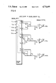
In FIG. 3 is shown an interface circuit in accordance with the foregoing description. It comprises a digital memory 1 which may be a PROM such as the type 82S123 manufactured by Signetics Corporation and having five inputs A0 -A4 and eight outputs D0 -D7. Conventional ROMS, EPROMS and other kinds of memories could also be employed. Memory 1 is conventionally powered so that a "1" bit is, for example, at a fixed potential and a "0" bit is at ground potential. If the power supply provides +5V, a "1" bit will be at that potential. The R, G, B and I bits of the digital color signals are respectively applied to inputs A0 -A3. The control bit C is provided by applying either ground or a +5V supply potential via a resistor to input terminal A4, a switch 2 being operable to selectively connect or disconnect terminal A4 to or from ground. Thus, operation of switch 2 sets the C bit to "0" and when not operated the C bit at terminal A4 is a "1". As described above with reference to the truth table in FIG. 2, this means that when switch 2 is not operated PROM 1 is set for translation of digital signals in the F1 color format and when switch 2 is operated PROM 1 is set for translation of digital signals in the F2 color format. The eight bits of the translate digital word corresponding to each input digital signal are produced at outputs D0 -D7 of PROM 1, in accordance with the truth table in FIG. 2. Outputs D0 -D2 are respectively connected by three attenuating elements such as resistors R0 -R2 to a summing terminal SR which is returned to ground by an attenuating element such as a resistor R10. Resistors R0 -R2 are proportioned to establish the requisite analog weighting factors for deriving the analog R color signal produced by the translator. Outputs D3 -D5 of PROM 1 are respectively connected by attenuating elements such as resistors R3 -R5 to a summing terminal SG which is returned to ground by an attenuating element such as a resistor R11. Resistors R3 -R5 are proportioned to establish the requisite analog weighting factors for deriving the analog G color output signal produced by the translator. Outputs D6 and D7 are respectively connected by attenuating elements such as resistors R6 and R7 to a summing terminal SB which is returned to ground by an attenuating element such as a resistor R12 and are proportioned to establish the requisite analog weighting factors for deriving the analog B color signal produced by the translator.
As noted above, the analog G signal requires 11 different weighting levels, which can be provided by least 4 attenuating elements. Accordingly, besides being utilized for color translation by PROM 1, the input digital signal G bit at input terminal A1 is also routed around PROM 1 and supplied through a buffer amplifier 4 and another attenuating element such as a resistor R8 directly to G summing terminal SG. Similarly, since the B analog signal requires 7 weighting levels, besides being utilized for color translation by PROM 1 the B bit of the digital signal at input terminal A2 is further routed around PROM 1 and supplied through a buffer amplifier 5 and an attenuating element such as a resistor R9 directly to B summing terminal SB. Resistors R8 and R9 are respectively proportioned relative to the other analog weighting resistors connected to terminals SG and SB, respectively, to establish the further analog weighting factors required for those signals as shown in FIGS. 1A and 1B.
Summing terminals SR, SG and SB are respectively connected to ground reference potential by resistors R10, R11, R12, and these are selected to have relatively low attenuation or resistance relative to each of the analog signal weighting resistors connected to the summing terminals. The voltages at those terminals will therefore respectively be proportional to the sum of the reciprocals of the resistances of the weighting resistors connected thereto. The analog summation voltages so produced at summing terminals SR, SG and SB are applied to the inputs of respective buffer amplifiers 6, 7 and 8 connected thereto, such as emitter follower transistor amplifiers, in order to obtain reduced output impedance. The output signals from amplifiers 6, 7 and 8 thereby constitute R, G and B analog signals for application to a video monitor CRT operating in the standard color format.
As indicated above, in the F1 color format the I bit of each digital signal affects the gray or luminence level of each of the analog color signals as well as the color hues corresponding thereto. However, in the case of the F2 color format the I bit only affects the color hues of the analog color signals. In order to take this difference into account, the I bit of the input digital color signal is also applied via an inverter 9 to an input of each of three NAND gates 10, 11, 12, the outputs of which are respectively connected by analog weighting elements such as resistors R13, R14, R15 to the respective analog summing terminals SR, SG, and SB. The signal attenuation or resistance of these resistors is set in such proportions relative to the other analog summing resistors connected to the corresponding running terminals to provide I signal weighting factors in accordance with color format F1 as shown in FIG. 1A. The control bit C, besides setting PROM 1 for color translation in accordance with either of color formats F1 and F2, is also utilized to gate the I signal. For that purpose, control bit C is applied to a second input of each of NAND gates 10, 11 and 12. Thus, when the control signal C is a "1", corresponding to color format F1, a "1" I bit will be inverted into a "0" by inverter 9 and applied to each of NAND gates 10, 11 and 12. These gates will therefore each produce a "1" output bit, or a +5V potential, and resistors R13, R14 and R15 will contribute to the resistive weightings effected at terminals SR, SG and SB. This effectively increases the voltage level corresponding to a "0" color signal summation at each such terminal from ground potential to approximately 33% of the maximum voltage which is produced thereat when all the color signal bits are "1", which corresponds to the effect of the I bit on the analog color signal weighting factors for color format F1 as shown in FIG. 1A.
When the control bit C is a "0", corresponding to color format F2, the outputs of NAND gates 10, 11 and 12 remain at "1", or +5V, regardless of whether the I bit is a "0" or a "1". Changes in the I signal therefore will not affect the analog color signal weightings effected by the resistive networks connected to terminals SR, SG and SB except insofar as the I bit enters into the digital word translation of the digital color signals effected by PROM 1.
The operation of the color interface circuit in FIG. 3 will be explained by two examples: translation of light blue in color format F2, and of brown in color format F1. These examples are respectively illustrated in FIGS. 4 and 5, wherein the block 10 labeled "decode logic" represents the portion of the complete interface circuit in FIG. 3 comprising PROM 1 and the interconnections of the G and B inputs thereto to the G auxiliary summing resistor R8 and the B auxiliary summing resistor R9.
Light blue in color format F2, as shown in the Truth Table in FIG. 2, is signified by a digital input signal 11100. Accordingly, these are the input digital signal bits in FIG. 4. Decode logic block 10 translates that digital signal to a digital word as shown in FIG. 2, which results in +5V on the outputs of logic block 10 corresponding to the "1" bits in the translated digital word. The remaining "0" outputs will be at ground potential. The analog voltage corresponding to summation of these digital voltages, weighted in proportion to the reciprocals of the resistances of the weighting resistors connected to these outputs, will be produced at terminals SR, SG and SB. These weighting proportions are set in accordance with the weighting factors shown in FIGS. 1A and 1B. By way of example, a suitable set of relative resistances of the various weighting resistors, and the corresponding inverse values or conductances thereof, is as follows:
______________________________________                                    
Weighting       Resistance                                                
                          Conductance                                     
Resistor        (K Ohms)  (10.sup.-3 Mhos)                                
______________________________________                                    
S.sub.R                                                                   
      R.sub.0       1.5       .67                                         
      R.sub.1       3.9       .26                                         
      R.sub.2       1.5       .67                                         
S.sub.G                                                                   
      R.sub.3       4.7       .213                                        
      R.sub.4       2.7       .37                                         
      R.sub.5       2.7       .37                                         
      R.sub.8       2.7       .37                                         
S.sub.B                                                                   
      R.sub.6       2.7       .37                                         
      R.sub.7       1.2       .83                                         
      R.sub.9       2.7       .37                                         
______________________________________                                    
The summed output voltage at any summing terminal is proportional to the sum of the conductances connected thereto. Accordingly, the maximum voltages at terminals SR, SG and SB will be respectively proportional to 1.60, 1.323 and 1.57.
In the example illustrated, the summed voltage at terminal SR will be proportional to the sum of the conductances of resistors R0 and R1, or 0.93×10⁻³ Mhos. This is 0.93/1.6=58% of the maximum output voltage at terminal SR, which is the relative amplitude of the R analog signal corresponding to the red primary color component of the standard R, G, B format in order to produce a light blue matching the light blue color of color format F2 as shown in FIG. 1B.
The summed voltage at terminal SG will be proportional to the sum of the conductances of resistors R3, R4 and R8, or 0.953×10⁻³ Mhos. This is 0.93/1.323=72% of the maximum output voltage terminal SG, which is the relative amplitude of the G analog signal corresponding to the green primary color component of the standard R, G, B format in order to produce the light blue of format F2.
In the case of the summed voltage at terminal SB, this will be at its maximum amplitude since all weighting resistors connected thereto are at +5V. Thus, its relative amplitude will be 100%, which is in agreement with the relative amplitude of the B analog signal necessar to produce the light blue color of color format F2 as shown in FIG. 1B.
It will therefore be apparent that the R, G and B analog output signals produced by the interface circuit in FIG. 3 in response to a digital input signal signifying the light blue color of color format F2 will be in the correct relative proportions to produce a matching light blue color on a video display monitor operating in the standard R, G, B color format.
FIG. 4 omits the resistors R13, R14 and R15 even though they are actually in the I signal bit paths connected to terminals SR, SG and SB as shown in FIG. 3. This is because, as explained above, when the control signal bit C is "0" the outputs of NAND gates 10, 11 and 12 remain at "1" regardless of the value of the digital I bit. Consequently, the presence of resistors R13, R14 and R15 does not alter the percentage changes in the magnitudes of the voltages at terminals SR, SG and SB in response to changes in the translated digital color signals.
Referring now to FIG. 5, illustrating production of the color brown in color format F1, the digital input signal as shown by the Truth Table in FIG. 2 is 11001. The corresponding translated digital word in FIG. 2 results in digital signals at the outputs of decode logic block 10 as shown in FIG. 5, including the "1" G signal routed to resistor R8 connected to G summing terminal SG and the "0" B signal routed to resistor R9 connected to the B summing terminal SB. FIG. 5 also includes the resistors R13, R14 and R15 which, as shown in FIG. 3, are connected to the respective summing terminals SR, SG and SB and to which the input digital I bit is routed after being inverted by inverter 9 and gated by NAND gates 10, 11 and 12 as described above. Since the control bit "C" is "1" for all colors in color format F1, and since for the color brown in that format the I bit is " 0", the NAND gates will apply ground potential to each of resistors R13, R14 and R15. The resistances of these resistors are proportioned in relation to the other weighting resistors connected to corresponding ones of summing terminals SR, SG and SB so as to obtain the analog color signal weightings shown in FIG. 1 for color format F1. Typical resistances of resistors R13, R14 and R15 are 1.2K Ohm, 3.4K Ohm and 1.2K Ohm. The sum of the conductances of all weighting resistors R0, R1, R2 and R13 connected to summing terminal SR is 2.43×10⁻³ Mhos, and the corresponding sums for summing terminals SG and SB are 1.61 and 2.4 respectively. Since only weighting resistors R0 and R1 connected to R summing terminal SR are at the "1" or +5V level, and the sum of their conductances is 1.60×10⁻³ Mhos, the summed voltage at terminal SR will be 1.60/2.43=66% of the maximum voltage at that terminal. A similar calculation for the weighting resistors connected to G summing terminal SG shows that the summed voltage thereat will be 46% of its maximum value. In the case of B summing terminal SB, since all of the weighting resistors connected thereto are at the "1" level the summed voltage thereat will be equal to 100% of its maximum value. These percentages agree with those shown in FIG. 1A for producing the color brown in format F1.
While the invention has been described with reference to certain specific embodiments thereof, it will be evident to those skilled in the art that many variations and modifications thereof may be made without departing from the true teachings and scope of the invention as defined in the succeeding claims.

Claims (5)

What is claimed is:
1. A color interface circuit for translating digital signals signifying colors in any of various color formats into analog signals for controlling respective primary colors of a video monitor displaying colors in a standard color format, one of the bits of each such signal signifying a grey intensity level; such circuit comprising:
digital memory means having stored therein a plurality of digital words respectively corresponding to the colors signified by the respective digital color signals, each such digital word having a predetermined number of bits, said memory means being adapted to read-out the digital word corresponding to any digital color signal upon receiving such digital color signal;
a plurality of digital word bit combining networks which respectively produce analog color signals corresponding to weighted summations of the bits of a digital word applied thereto, such analog signals respectively corresponding to the respective primary colors of said video monitor, said combining networks being connected to said memory means to receive the bits of the digital word read-out therefrom in response to a digital color signal received thereby; each of said combining networks weighting the bits of a digital word applied thereto so that the relative proportions of the weighted analog summations thereof match the relative proportions of the primary colors of said video monitor for displaying the color signified by the digital color signal received by said memory means;
switching means connected to said digital memory means for adding at least one control bit to each of the digital color signals received thereby, said switching means being operable to set the digital value of each such control bit in correspondence with the color format of the received digital color signals; whereby the digital word read-out from said memory means in response to a received digital color signal can be altered by said switching means so as to correspond with the particular color format of such received digital color signal;
a signal attenuating element in each of said combining networks for receiving said grey intensity level bit of a received digital color signal; and
gating means controlled by the control bits added to the received digital color signal for gating the application of said grey intensity level bit to said grey level signal attenuating elements in said conbining networks; whereby the relative proportions of the analog signals produced by said combining networks are adjusted in accordance with the effect of said grey intensity level bit on the colors signified by the received digital color signal.
2. A color interface circuit in accordance with claim 1, wherein each of said combining networks comprises a plurality of signal attenuating elements to which the bits of a digital word read-out from said memory means are respectively applied, the relative signal attenuations of such attenuating elements being proportioned so as to produce said weighted summations of the bits of said digital word.
3. A color interface circuit in accordance with claim 2, wherein said signal attenuating elements are resistor means.
4. A color interface circuit in accordance with claim 1, wherein said gating means comprises:
an inverter for inverting said gray intensity level bit; and
a plurality of NAND circuits respectively having a first input connected to said inverter, a second input connected to said switching means, and an output connected to one of said combining networks.
5. A color interface circuit in accordance with claim 4, wherein said memory means is a solid-state programmable read-only memory.
US06/903,006 1986-09-02 1986-09-02 Video monitor interface circuit for digital color signals Expired - Fee Related US4774495A (en)

Priority Applications (4)

Application Number Priority Date Filing Date Title
US06/903,006 US4774495A (en) 1986-09-02 1986-09-02 Video monitor interface circuit for digital color signals
JP62215532A JPS63118189A (en) 1986-09-02 1987-08-31 Video monitor interface circuit for digital color signal
KR870009553A KR880004687A (en) 1986-09-02 1987-08-31 Color Interface Circuits for Digital Color Signals
EP19870201647 EP0258947A3 (en) 1986-09-02 1987-08-31 Video monitor interface circuit for digital color signals

Applications Claiming Priority (1)

Application Number Priority Date Filing Date Title
US06/903,006 US4774495A (en) 1986-09-02 1986-09-02 Video monitor interface circuit for digital color signals

Publications (1)

Publication Number Publication Date
US4774495A true US4774495A (en) 1988-09-27

Family

ID=25416772

Family Applications (1)

Application Number Title Priority Date Filing Date
US06/903,006 Expired - Fee Related US4774495A (en) 1986-09-02 1986-09-02 Video monitor interface circuit for digital color signals

Country Status (4)

Country Link
US (1) US4774495A (en)
EP (1) EP0258947A3 (en)
JP (1) JPS63118189A (en)
KR (1) KR880004687A (en)

Cited By (2)

* Cited by examiner, † Cited by third party
Publication number Priority date Publication date Assignee Title
US4920344A (en) * 1985-03-11 1990-04-24 Ncr Corporation Digitally compensated multiplying digital to analog converter
US5313300A (en) * 1992-08-10 1994-05-17 Commodore Electronics Limited Binary to unary decoder for a video digital to analog converter

Citations (3)

* Cited by examiner, † Cited by third party
Publication number Priority date Publication date Assignee Title
US3744050A (en) * 1970-11-23 1973-07-03 Lear Siegler Inc Apparatus for providing an analog output in response to a digital input
US4216460A (en) * 1977-07-14 1980-08-05 Independent Broadcasting Authority Transmission and/or recording of digital signals
US4547797A (en) * 1982-10-12 1985-10-15 Sperry Corporation Apparatus for color tracking and brightness correction for multi-gun color cathode ray tube display

Family Cites Families (3)

* Cited by examiner, † Cited by third party
Publication number Priority date Publication date Assignee Title
US4590463A (en) * 1980-09-29 1986-05-20 Rca Corporation Digital control of color in CRT display
US4386345A (en) * 1981-09-22 1983-05-31 Sperry Corporation Color and brightness tracking in a cathode ray tube display system
GB2167926A (en) * 1984-11-26 1986-06-04 Philips Nv Colour signal generator for crt image display

Patent Citations (3)

* Cited by examiner, † Cited by third party
Publication number Priority date Publication date Assignee Title
US3744050A (en) * 1970-11-23 1973-07-03 Lear Siegler Inc Apparatus for providing an analog output in response to a digital input
US4216460A (en) * 1977-07-14 1980-08-05 Independent Broadcasting Authority Transmission and/or recording of digital signals
US4547797A (en) * 1982-10-12 1985-10-15 Sperry Corporation Apparatus for color tracking and brightness correction for multi-gun color cathode ray tube display

Cited By (2)

* Cited by examiner, † Cited by third party
Publication number Priority date Publication date Assignee Title
US4920344A (en) * 1985-03-11 1990-04-24 Ncr Corporation Digitally compensated multiplying digital to analog converter
US5313300A (en) * 1992-08-10 1994-05-17 Commodore Electronics Limited Binary to unary decoder for a video digital to analog converter

Also Published As

Publication number Publication date
EP0258947A3 (en) 1990-10-17
KR880004687A (en) 1988-06-07
JPS63118189A (en) 1988-05-23
EP0258947A2 (en) 1988-03-09

Similar Documents

Publication Publication Date Title
US5757298A (en) Method and apparatus for error compensation using a non-linear digital-to-analog converter
US4639771A (en) Image processing system
US4868571A (en) Digital to analog converter
CA1324847C (en) Color graphics system
JPH058438B2 (en)
US4695826A (en) High accuracy digital-to-analog converter having symmetrical current source switching
US4831571A (en) Barrel shifter for rotating data with or without carry
WO1993004461A1 (en) High speed ramdac with reconfigurable color palette
US4727414A (en) Circuit for converting digital signals representing color information into analog voltage level signals with enhanced contrast between foreground and background
US5638090A (en) Window-dependent brightness/tint control for video digital-to-analog converters
US4774495A (en) Video monitor interface circuit for digital color signals
GB2223149A (en) Digital data display system
US4626835A (en) RGBI digital video control system having intensity level control and overall image strength control
US4779029A (en) Digitally compensated multiplying digital to analog converter
US4920344A (en) Digitally compensated multiplying digital to analog converter
US5012342A (en) Video prioritizer and mixer
CA1298422C (en) Monitor interface circuit
JPH02130586A (en) Liquid crystal display driving device
US4860235A (en) Arithmetic unit with alternate mark inversion (AMI) coding
US4990915A (en) Signal processing device such as a digital filter utilizing redundant binary expression and operating method therefor
US4084252A (en) Current mode 5-bit arithmetic logic unit with parity
US4974070A (en) Colorgraphic reproduction system
US4079457A (en) Current mode binary/BCD arithmetic logic unit with parity
USRE26780E (en) Electronic diode matrix decoder circuits
JP2680940B2 (en) D / A converter

Legal Events

Date Code Title Description
AS Assignment

Owner name: NORTH AMERICAN PHILIPS CONSUMER ELECTRONICS CORPOR

Free format text: ASSIGNMENT OF ASSIGNORS INTEREST.;ASSIGNORS:RAFTER, PATRICK M.;WOLTER, DONALD B.;REEL/FRAME:004597/0796

Effective date: 19860828

Owner name: NORTH AMERICAN PHILIPS CONSUMER ELECTRONICS CORPOR

Free format text: ASSIGNMENT OF ASSIGNORS INTEREST;ASSIGNORS:RAFTER, PATRICK M.;WOLTER, DONALD B.;REEL/FRAME:004597/0796

Effective date: 19860828

FPAY Fee payment

Year of fee payment: 4

REMI Maintenance fee reminder mailed
LAPS Lapse for failure to pay maintenance fees
FP Lapsed due to failure to pay maintenance fee

Effective date: 19961002

STCH Information on status: patent discontinuation

Free format text: PATENT EXPIRED DUE TO NONPAYMENT OF MAINTENANCE FEES UNDER 37 CFR 1.362