EP0258752A2 - Anordnung mit einer Oberflächenschicht, die gleichmässig orientierte, kristalline, organische Mikrostrukturen enthält - Google Patents
Anordnung mit einer Oberflächenschicht, die gleichmässig orientierte, kristalline, organische Mikrostrukturen enthält Download PDFInfo
- Publication number
- EP0258752A2 EP0258752A2 EP87112108A EP87112108A EP0258752A2 EP 0258752 A2 EP0258752 A2 EP 0258752A2 EP 87112108 A EP87112108 A EP 87112108A EP 87112108 A EP87112108 A EP 87112108A EP 0258752 A2 EP0258752 A2 EP 0258752A2
- Authority
- EP
- European Patent Office
- Prior art keywords
- microstructures
- article according
- article
- substrate
- organic
- Prior art date
- Legal status (The legal status is an assumption and is not a legal conclusion. Google has not performed a legal analysis and makes no representation as to the accuracy of the status listed.)
- Granted
Links
- 239000002344 surface layer Substances 0.000 title 1
- 239000000758 substrate Substances 0.000 claims abstract description 74
- 238000000034 method Methods 0.000 claims abstract description 30
- 238000000137 annealing Methods 0.000 claims abstract description 25
- 239000000463 material Substances 0.000 claims abstract description 20
- 238000000151 deposition Methods 0.000 claims abstract description 19
- 150000002894 organic compounds Chemical class 0.000 claims abstract description 5
- 239000007787 solid Substances 0.000 claims abstract description 5
- 229910052751 metal Inorganic materials 0.000 claims description 29
- 239000002184 metal Substances 0.000 claims description 29
- 239000011368 organic material Substances 0.000 claims description 29
- 150000004032 porphyrins Chemical class 0.000 claims description 6
- 125000006615 aromatic heterocyclic group Chemical group 0.000 claims description 5
- 229920005547 polycyclic aromatic hydrocarbon Polymers 0.000 claims description 5
- 229910010272 inorganic material Inorganic materials 0.000 claims description 4
- 239000011147 inorganic material Substances 0.000 claims description 4
- 150000002979 perylenes Chemical class 0.000 claims description 3
- IEQIEDJGQAUEQZ-UHFFFAOYSA-N phthalocyanine Chemical compound N1C(N=C2C3=CC=CC=C3C(N=C3C4=CC=CC=C4C(=N4)N3)=N2)=C(C=CC=C2)C2=C1N=C1C2=CC=CC=C2C4=N1 IEQIEDJGQAUEQZ-UHFFFAOYSA-N 0.000 claims description 3
- WLLGXSLBOPFWQV-UHFFFAOYSA-N MGK 264 Chemical compound C1=CC2CC1C1C2C(=O)N(CC(CC)CCCC)C1=O WLLGXSLBOPFWQV-UHFFFAOYSA-N 0.000 claims description 2
- 150000001491 aromatic compounds Chemical class 0.000 claims description 2
- 239000002131 composite material Substances 0.000 abstract description 16
- 230000008569 process Effects 0.000 abstract description 15
- 238000002310 reflectometry Methods 0.000 abstract description 14
- 238000010521 absorption reaction Methods 0.000 abstract description 9
- 230000008859 change Effects 0.000 abstract description 6
- 230000003287 optical effect Effects 0.000 abstract description 6
- 238000003860 storage Methods 0.000 abstract description 5
- 230000005540 biological transmission Effects 0.000 abstract description 3
- 238000009826 distribution Methods 0.000 abstract description 3
- 238000003384 imaging method Methods 0.000 abstract description 3
- 230000007797 corrosion Effects 0.000 abstract description 2
- 238000005260 corrosion Methods 0.000 abstract description 2
- 230000005670 electromagnetic radiation Effects 0.000 abstract description 2
- 239000010408 film Substances 0.000 description 45
- ZZSIDSMUTXFKNS-UHFFFAOYSA-N perylene red Chemical compound CC(C)C1=CC=CC(C(C)C)=C1N(C(=O)C=1C2=C3C4=C(OC=5C=CC=CC=5)C=1)C(=O)C2=CC(OC=1C=CC=CC=1)=C3C(C(OC=1C=CC=CC=1)=CC1=C2C(C(N(C=3C(=CC=CC=3C(C)C)C(C)C)C1=O)=O)=C1)=C2C4=C1OC1=CC=CC=C1 ZZSIDSMUTXFKNS-UHFFFAOYSA-N 0.000 description 28
- 238000000576 coating method Methods 0.000 description 24
- 239000011248 coating agent Substances 0.000 description 23
- RYGMFSIKBFXOCR-UHFFFAOYSA-N Copper Chemical compound [Cu] RYGMFSIKBFXOCR-UHFFFAOYSA-N 0.000 description 22
- 229910052802 copper Inorganic materials 0.000 description 22
- 239000010949 copper Substances 0.000 description 22
- BASFCYQUMIYNBI-UHFFFAOYSA-N platinum Chemical compound [Pt] BASFCYQUMIYNBI-UHFFFAOYSA-N 0.000 description 18
- 229910052782 aluminium Inorganic materials 0.000 description 15
- XAGFODPZIPBFFR-UHFFFAOYSA-N aluminium Chemical compound [Al] XAGFODPZIPBFFR-UHFFFAOYSA-N 0.000 description 15
- 239000010410 layer Substances 0.000 description 14
- 238000007740 vapor deposition Methods 0.000 description 13
- 239000004698 Polyethylene Substances 0.000 description 12
- -1 polyethylene Polymers 0.000 description 12
- 229920000573 polyethylene Polymers 0.000 description 12
- 230000008021 deposition Effects 0.000 description 11
- 239000011521 glass Substances 0.000 description 11
- 238000010438 heat treatment Methods 0.000 description 10
- 239000010453 quartz Substances 0.000 description 10
- VYPSYNLAJGMNEJ-UHFFFAOYSA-N silicon dioxide Inorganic materials O=[Si]=O VYPSYNLAJGMNEJ-UHFFFAOYSA-N 0.000 description 10
- 229910052697 platinum Inorganic materials 0.000 description 9
- 239000000126 substance Substances 0.000 description 9
- 239000013078 crystal Substances 0.000 description 6
- 150000001875 compounds Chemical class 0.000 description 5
- 150000002739 metals Chemical class 0.000 description 5
- 238000001878 scanning electron micrograph Methods 0.000 description 5
- IJGRMHOSHXDMSA-UHFFFAOYSA-N Atomic nitrogen Chemical compound N#N IJGRMHOSHXDMSA-UHFFFAOYSA-N 0.000 description 4
- RBTKNAXYKSUFRK-UHFFFAOYSA-N heliogen blue Chemical compound [Cu].[N-]1C2=C(C=CC=C3)C3=C1N=C([N-]1)C3=CC=CC=C3C1=NC([N-]1)=C(C=CC=C3)C3=C1N=C([N-]1)C3=CC=CC=C3C1=N2 RBTKNAXYKSUFRK-UHFFFAOYSA-N 0.000 description 4
- 238000000859 sublimation Methods 0.000 description 4
- 230000008022 sublimation Effects 0.000 description 4
- 238000001771 vacuum deposition Methods 0.000 description 4
- WSFSSNUMVMOOMR-UHFFFAOYSA-N Formaldehyde Chemical compound O=C WSFSSNUMVMOOMR-UHFFFAOYSA-N 0.000 description 3
- 239000012298 atmosphere Substances 0.000 description 3
- 238000002129 infrared reflectance spectroscopy Methods 0.000 description 3
- 150000002500 ions Chemical class 0.000 description 3
- 238000004519 manufacturing process Methods 0.000 description 3
- 239000000203 mixture Substances 0.000 description 3
- 238000004544 sputter deposition Methods 0.000 description 3
- 238000000427 thin-film deposition Methods 0.000 description 3
- WFKWXMTUELFFGS-UHFFFAOYSA-N tungsten Chemical compound [W] WFKWXMTUELFFGS-UHFFFAOYSA-N 0.000 description 3
- PXHVJJICTQNCMI-UHFFFAOYSA-N Nickel Chemical compound [Ni] PXHVJJICTQNCMI-UHFFFAOYSA-N 0.000 description 2
- WCUXLLCKKVVCTQ-UHFFFAOYSA-M Potassium chloride Chemical compound [Cl-].[K+] WCUXLLCKKVVCTQ-UHFFFAOYSA-M 0.000 description 2
- 238000003917 TEM image Methods 0.000 description 2
- 230000002411 adverse Effects 0.000 description 2
- 229910045601 alloy Inorganic materials 0.000 description 2
- 239000000956 alloy Substances 0.000 description 2
- PNEYBMLMFCGWSK-UHFFFAOYSA-N aluminium oxide Inorganic materials [O-2].[O-2].[O-2].[Al+3].[Al+3] PNEYBMLMFCGWSK-UHFFFAOYSA-N 0.000 description 2
- 230000015572 biosynthetic process Effects 0.000 description 2
- 238000001311 chemical methods and process Methods 0.000 description 2
- 238000001816 cooling Methods 0.000 description 2
- VVOLVFOSOPJKED-UHFFFAOYSA-N copper phthalocyanine Chemical compound [Cu].N=1C2=NC(C3=CC=CC=C33)=NC3=NC(C3=CC=CC=C33)=NC3=NC(C3=CC=CC=C33)=NC3=NC=1C1=CC=CC=C12 VVOLVFOSOPJKED-UHFFFAOYSA-N 0.000 description 2
- 230000007547 defect Effects 0.000 description 2
- 230000001419 dependent effect Effects 0.000 description 2
- 238000009792 diffusion process Methods 0.000 description 2
- 238000001035 drying Methods 0.000 description 2
- 239000005329 float glass Substances 0.000 description 2
- 239000007788 liquid Substances 0.000 description 2
- 229910044991 metal oxide Inorganic materials 0.000 description 2
- 150000004706 metal oxides Chemical class 0.000 description 2
- 229910001120 nichrome Inorganic materials 0.000 description 2
- 229910052757 nitrogen Inorganic materials 0.000 description 2
- 238000001020 plasma etching Methods 0.000 description 2
- 230000003595 spectral effect Effects 0.000 description 2
- 239000010409 thin film Substances 0.000 description 2
- 229910052721 tungsten Inorganic materials 0.000 description 2
- 239000010937 tungsten Substances 0.000 description 2
- 238000007704 wet chemistry method Methods 0.000 description 2
- 238000004566 IR spectroscopy Methods 0.000 description 1
- FYYHWMGAXLPEAU-UHFFFAOYSA-N Magnesium Chemical compound [Mg] FYYHWMGAXLPEAU-UHFFFAOYSA-N 0.000 description 1
- ZOKXTWBITQBERF-UHFFFAOYSA-N Molybdenum Chemical compound [Mo] ZOKXTWBITQBERF-UHFFFAOYSA-N 0.000 description 1
- HCHKCACWOHOZIP-UHFFFAOYSA-N Zinc Chemical compound [Zn] HCHKCACWOHOZIP-UHFFFAOYSA-N 0.000 description 1
- 239000006096 absorbing agent Substances 0.000 description 1
- 230000004075 alteration Effects 0.000 description 1
- 238000007743 anodising Methods 0.000 description 1
- 150000001454 anthracenes Chemical class 0.000 description 1
- 239000012300 argon atmosphere Substances 0.000 description 1
- 235000015241 bacon Nutrition 0.000 description 1
- 230000008901 benefit Effects 0.000 description 1
- 229910001593 boehmite Inorganic materials 0.000 description 1
- 150000001716 carbazoles Chemical class 0.000 description 1
- 239000000919 ceramic Substances 0.000 description 1
- 238000005234 chemical deposition Methods 0.000 description 1
- 238000003486 chemical etching Methods 0.000 description 1
- 238000006243 chemical reaction Methods 0.000 description 1
- 229910017052 cobalt Inorganic materials 0.000 description 1
- 239000010941 cobalt Substances 0.000 description 1
- GUTLYIVDDKVIGB-UHFFFAOYSA-N cobalt atom Chemical compound [Co] GUTLYIVDDKVIGB-UHFFFAOYSA-N 0.000 description 1
- 150000001882 coronenes Chemical class 0.000 description 1
- 239000002178 crystalline material Substances 0.000 description 1
- 238000007872 degassing Methods 0.000 description 1
- 230000001627 detrimental effect Effects 0.000 description 1
- 238000010586 diagram Methods 0.000 description 1
- 238000007598 dipping method Methods 0.000 description 1
- 230000000694 effects Effects 0.000 description 1
- 238000005530 etching Methods 0.000 description 1
- 239000007789 gas Substances 0.000 description 1
- 150000002391 heterocyclic compounds Chemical class 0.000 description 1
- FAHBNUUHRFUEAI-UHFFFAOYSA-M hydroxidooxidoaluminium Chemical compound O[Al]=O FAHBNUUHRFUEAI-UHFFFAOYSA-M 0.000 description 1
- 238000011065 in-situ storage Methods 0.000 description 1
- 230000000977 initiatory effect Effects 0.000 description 1
- 238000007689 inspection Methods 0.000 description 1
- 229910052749 magnesium Inorganic materials 0.000 description 1
- 239000011777 magnesium Substances 0.000 description 1
- 238000005259 measurement Methods 0.000 description 1
- 230000007246 mechanism Effects 0.000 description 1
- 239000007769 metal material Substances 0.000 description 1
- 230000004048 modification Effects 0.000 description 1
- 238000012986 modification Methods 0.000 description 1
- 229910052750 molybdenum Inorganic materials 0.000 description 1
- 239000011733 molybdenum Substances 0.000 description 1
- 150000002790 naphthalenes Chemical class 0.000 description 1
- 229910052759 nickel Inorganic materials 0.000 description 1
- 239000012044 organic layer Substances 0.000 description 1
- 230000001590 oxidative effect Effects 0.000 description 1
- 238000009304 pastoral farming Methods 0.000 description 1
- 239000008188 pellet Substances 0.000 description 1
- 150000002987 phenanthrenes Chemical class 0.000 description 1
- 238000005289 physical deposition Methods 0.000 description 1
- 229920003023 plastic Polymers 0.000 description 1
- 239000004033 plastic Substances 0.000 description 1
- 229920000642 polymer Polymers 0.000 description 1
- 239000001103 potassium chloride Substances 0.000 description 1
- 235000011164 potassium chloride Nutrition 0.000 description 1
- 230000002028 premature Effects 0.000 description 1
- 239000011253 protective coating Substances 0.000 description 1
- 150000003212 purines Chemical class 0.000 description 1
- 150000003220 pyrenes Chemical class 0.000 description 1
- 230000005855 radiation Effects 0.000 description 1
- 239000001054 red pigment Substances 0.000 description 1
- 229920006395 saturated elastomer Polymers 0.000 description 1
- 238000004626 scanning electron microscopy Methods 0.000 description 1
- 238000012306 spectroscopic technique Methods 0.000 description 1
- 238000001228 spectrum Methods 0.000 description 1
- 238000005507 spraying Methods 0.000 description 1
- 238000000992 sputter etching Methods 0.000 description 1
- JVTCNOASZYIKTG-UHFFFAOYSA-N stk329495 Chemical compound [Cu].[N-]1C(N=C2C3=CC=CC=C3C(N=C3C4=CC=CC=C4C(=N4)[N-]3)=N2)=C(C=CC=C2)C2=C1N=C1C2=CC=CC=C2C4=N1 JVTCNOASZYIKTG-UHFFFAOYSA-N 0.000 description 1
- 229910052715 tantalum Inorganic materials 0.000 description 1
- GUVRBAGPIYLISA-UHFFFAOYSA-N tantalum atom Chemical compound [Ta] GUVRBAGPIYLISA-UHFFFAOYSA-N 0.000 description 1
- 230000007704 transition Effects 0.000 description 1
- 238000002834 transmittance Methods 0.000 description 1
- 229920002554 vinyl polymer Polymers 0.000 description 1
- 230000000007 visual effect Effects 0.000 description 1
- XLYOFNOQVPJJNP-UHFFFAOYSA-N water Substances O XLYOFNOQVPJJNP-UHFFFAOYSA-N 0.000 description 1
- 239000011701 zinc Substances 0.000 description 1
- 229910052725 zinc Inorganic materials 0.000 description 1
Images


Classifications
-
- C—CHEMISTRY; METALLURGY
- C23—COATING METALLIC MATERIAL; COATING MATERIAL WITH METALLIC MATERIAL; CHEMICAL SURFACE TREATMENT; DIFFUSION TREATMENT OF METALLIC MATERIAL; COATING BY VACUUM EVAPORATION, BY SPUTTERING, BY ION IMPLANTATION OR BY CHEMICAL VAPOUR DEPOSITION, IN GENERAL; INHIBITING CORROSION OF METALLIC MATERIAL OR INCRUSTATION IN GENERAL
- C23C—COATING METALLIC MATERIAL; COATING MATERIAL WITH METALLIC MATERIAL; SURFACE TREATMENT OF METALLIC MATERIAL BY DIFFUSION INTO THE SURFACE, BY CHEMICAL CONVERSION OR SUBSTITUTION; COATING BY VACUUM EVAPORATION, BY SPUTTERING, BY ION IMPLANTATION OR BY CHEMICAL VAPOUR DEPOSITION, IN GENERAL
- C23C14/00—Coating by vacuum evaporation, by sputtering or by ion implantation of the coating forming material
- C23C14/58—After-treatment
- C23C14/5806—Thermal treatment
-
- C—CHEMISTRY; METALLURGY
- C23—COATING METALLIC MATERIAL; COATING MATERIAL WITH METALLIC MATERIAL; CHEMICAL SURFACE TREATMENT; DIFFUSION TREATMENT OF METALLIC MATERIAL; COATING BY VACUUM EVAPORATION, BY SPUTTERING, BY ION IMPLANTATION OR BY CHEMICAL VAPOUR DEPOSITION, IN GENERAL; INHIBITING CORROSION OF METALLIC MATERIAL OR INCRUSTATION IN GENERAL
- C23C—COATING METALLIC MATERIAL; COATING MATERIAL WITH METALLIC MATERIAL; SURFACE TREATMENT OF METALLIC MATERIAL BY DIFFUSION INTO THE SURFACE, BY CHEMICAL CONVERSION OR SUBSTITUTION; COATING BY VACUUM EVAPORATION, BY SPUTTERING, BY ION IMPLANTATION OR BY CHEMICAL VAPOUR DEPOSITION, IN GENERAL
- C23C14/00—Coating by vacuum evaporation, by sputtering or by ion implantation of the coating forming material
- C23C14/06—Coating by vacuum evaporation, by sputtering or by ion implantation of the coating forming material characterised by the coating material
- C23C14/12—Organic material
-
- C—CHEMISTRY; METALLURGY
- C23—COATING METALLIC MATERIAL; COATING MATERIAL WITH METALLIC MATERIAL; CHEMICAL SURFACE TREATMENT; DIFFUSION TREATMENT OF METALLIC MATERIAL; COATING BY VACUUM EVAPORATION, BY SPUTTERING, BY ION IMPLANTATION OR BY CHEMICAL VAPOUR DEPOSITION, IN GENERAL; INHIBITING CORROSION OF METALLIC MATERIAL OR INCRUSTATION IN GENERAL
- C23C—COATING METALLIC MATERIAL; COATING MATERIAL WITH METALLIC MATERIAL; SURFACE TREATMENT OF METALLIC MATERIAL BY DIFFUSION INTO THE SURFACE, BY CHEMICAL CONVERSION OR SUBSTITUTION; COATING BY VACUUM EVAPORATION, BY SPUTTERING, BY ION IMPLANTATION OR BY CHEMICAL VAPOUR DEPOSITION, IN GENERAL
- C23C14/00—Coating by vacuum evaporation, by sputtering or by ion implantation of the coating forming material
- C23C14/06—Coating by vacuum evaporation, by sputtering or by ion implantation of the coating forming material characterised by the coating material
- C23C14/14—Metallic material, boron or silicon
- C23C14/20—Metallic material, boron or silicon on organic substrates
-
- C—CHEMISTRY; METALLURGY
- C23—COATING METALLIC MATERIAL; COATING MATERIAL WITH METALLIC MATERIAL; CHEMICAL SURFACE TREATMENT; DIFFUSION TREATMENT OF METALLIC MATERIAL; COATING BY VACUUM EVAPORATION, BY SPUTTERING, BY ION IMPLANTATION OR BY CHEMICAL VAPOUR DEPOSITION, IN GENERAL; INHIBITING CORROSION OF METALLIC MATERIAL OR INCRUSTATION IN GENERAL
- C23C—COATING METALLIC MATERIAL; COATING MATERIAL WITH METALLIC MATERIAL; SURFACE TREATMENT OF METALLIC MATERIAL BY DIFFUSION INTO THE SURFACE, BY CHEMICAL CONVERSION OR SUBSTITUTION; COATING BY VACUUM EVAPORATION, BY SPUTTERING, BY ION IMPLANTATION OR BY CHEMICAL VAPOUR DEPOSITION, IN GENERAL
- C23C14/00—Coating by vacuum evaporation, by sputtering or by ion implantation of the coating forming material
- C23C14/58—After-treatment
- C23C14/584—Non-reactive treatment
-
- C—CHEMISTRY; METALLURGY
- C30—CRYSTAL GROWTH
- C30B—SINGLE-CRYSTAL GROWTH; UNIDIRECTIONAL SOLIDIFICATION OF EUTECTIC MATERIAL OR UNIDIRECTIONAL DEMIXING OF EUTECTOID MATERIAL; REFINING BY ZONE-MELTING OF MATERIAL; PRODUCTION OF A HOMOGENEOUS POLYCRYSTALLINE MATERIAL WITH DEFINED STRUCTURE; SINGLE CRYSTALS OR HOMOGENEOUS POLYCRYSTALLINE MATERIAL WITH DEFINED STRUCTURE; AFTER-TREATMENT OF SINGLE CRYSTALS OR A HOMOGENEOUS POLYCRYSTALLINE MATERIAL WITH DEFINED STRUCTURE; APPARATUS THEREFOR
- C30B23/00—Single-crystal growth by condensing evaporated or sublimed materials
- C30B23/007—Growth of whiskers or needles
-
- C—CHEMISTRY; METALLURGY
- C30—CRYSTAL GROWTH
- C30B—SINGLE-CRYSTAL GROWTH; UNIDIRECTIONAL SOLIDIFICATION OF EUTECTIC MATERIAL OR UNIDIRECTIONAL DEMIXING OF EUTECTOID MATERIAL; REFINING BY ZONE-MELTING OF MATERIAL; PRODUCTION OF A HOMOGENEOUS POLYCRYSTALLINE MATERIAL WITH DEFINED STRUCTURE; SINGLE CRYSTALS OR HOMOGENEOUS POLYCRYSTALLINE MATERIAL WITH DEFINED STRUCTURE; AFTER-TREATMENT OF SINGLE CRYSTALS OR A HOMOGENEOUS POLYCRYSTALLINE MATERIAL WITH DEFINED STRUCTURE; APPARATUS THEREFOR
- C30B25/00—Single-crystal growth by chemical reaction of reactive gases, e.g. chemical vapour-deposition growth
- C30B25/005—Growth of whiskers or needles
-
- C—CHEMISTRY; METALLURGY
- C30—CRYSTAL GROWTH
- C30B—SINGLE-CRYSTAL GROWTH; UNIDIRECTIONAL SOLIDIFICATION OF EUTECTIC MATERIAL OR UNIDIRECTIONAL DEMIXING OF EUTECTOID MATERIAL; REFINING BY ZONE-MELTING OF MATERIAL; PRODUCTION OF A HOMOGENEOUS POLYCRYSTALLINE MATERIAL WITH DEFINED STRUCTURE; SINGLE CRYSTALS OR HOMOGENEOUS POLYCRYSTALLINE MATERIAL WITH DEFINED STRUCTURE; AFTER-TREATMENT OF SINGLE CRYSTALS OR A HOMOGENEOUS POLYCRYSTALLINE MATERIAL WITH DEFINED STRUCTURE; APPARATUS THEREFOR
- C30B29/00—Single crystals or homogeneous polycrystalline material with defined structure characterised by the material or by their shape
- C30B29/54—Organic compounds
-
- C—CHEMISTRY; METALLURGY
- C30—CRYSTAL GROWTH
- C30B—SINGLE-CRYSTAL GROWTH; UNIDIRECTIONAL SOLIDIFICATION OF EUTECTIC MATERIAL OR UNIDIRECTIONAL DEMIXING OF EUTECTOID MATERIAL; REFINING BY ZONE-MELTING OF MATERIAL; PRODUCTION OF A HOMOGENEOUS POLYCRYSTALLINE MATERIAL WITH DEFINED STRUCTURE; SINGLE CRYSTALS OR HOMOGENEOUS POLYCRYSTALLINE MATERIAL WITH DEFINED STRUCTURE; AFTER-TREATMENT OF SINGLE CRYSTALS OR A HOMOGENEOUS POLYCRYSTALLINE MATERIAL WITH DEFINED STRUCTURE; APPARATUS THEREFOR
- C30B29/00—Single crystals or homogeneous polycrystalline material with defined structure characterised by the material or by their shape
- C30B29/60—Single crystals or homogeneous polycrystalline material with defined structure characterised by the material or by their shape characterised by shape
- C30B29/62—Whiskers or needles
-
- C—CHEMISTRY; METALLURGY
- C30—CRYSTAL GROWTH
- C30B—SINGLE-CRYSTAL GROWTH; UNIDIRECTIONAL SOLIDIFICATION OF EUTECTIC MATERIAL OR UNIDIRECTIONAL DEMIXING OF EUTECTOID MATERIAL; REFINING BY ZONE-MELTING OF MATERIAL; PRODUCTION OF A HOMOGENEOUS POLYCRYSTALLINE MATERIAL WITH DEFINED STRUCTURE; SINGLE CRYSTALS OR HOMOGENEOUS POLYCRYSTALLINE MATERIAL WITH DEFINED STRUCTURE; AFTER-TREATMENT OF SINGLE CRYSTALS OR A HOMOGENEOUS POLYCRYSTALLINE MATERIAL WITH DEFINED STRUCTURE; APPARATUS THEREFOR
- C30B33/00—After-treatment of single crystals or homogeneous polycrystalline material with defined structure
-
- F—MECHANICAL ENGINEERING; LIGHTING; HEATING; WEAPONS; BLASTING
- F24—HEATING; RANGES; VENTILATING
- F24S—SOLAR HEAT COLLECTORS; SOLAR HEAT SYSTEMS
- F24S70/00—Details of absorbing elements
- F24S70/20—Details of absorbing elements characterised by absorbing coatings; characterised by surface treatment for increasing absorption
- F24S70/225—Details of absorbing elements characterised by absorbing coatings; characterised by surface treatment for increasing absorption for spectrally selective absorption
-
- F—MECHANICAL ENGINEERING; LIGHTING; HEATING; WEAPONS; BLASTING
- F24—HEATING; RANGES; VENTILATING
- F24S—SOLAR HEAT COLLECTORS; SOLAR HEAT SYSTEMS
- F24S70/00—Details of absorbing elements
- F24S70/60—Details of absorbing elements characterised by the structure or construction
-
- Y—GENERAL TAGGING OF NEW TECHNOLOGICAL DEVELOPMENTS; GENERAL TAGGING OF CROSS-SECTIONAL TECHNOLOGIES SPANNING OVER SEVERAL SECTIONS OF THE IPC; TECHNICAL SUBJECTS COVERED BY FORMER USPC CROSS-REFERENCE ART COLLECTIONS [XRACs] AND DIGESTS
- Y02—TECHNOLOGIES OR APPLICATIONS FOR MITIGATION OR ADAPTATION AGAINST CLIMATE CHANGE
- Y02E—REDUCTION OF GREENHOUSE GAS [GHG] EMISSIONS, RELATED TO ENERGY GENERATION, TRANSMISSION OR DISTRIBUTION
- Y02E10/00—Energy generation through renewable energy sources
- Y02E10/40—Solar thermal energy, e.g. solar towers
- Y02E10/44—Heat exchange systems
-
- Y—GENERAL TAGGING OF NEW TECHNOLOGICAL DEVELOPMENTS; GENERAL TAGGING OF CROSS-SECTIONAL TECHNOLOGIES SPANNING OVER SEVERAL SECTIONS OF THE IPC; TECHNICAL SUBJECTS COVERED BY FORMER USPC CROSS-REFERENCE ART COLLECTIONS [XRACs] AND DIGESTS
- Y10—TECHNICAL SUBJECTS COVERED BY FORMER USPC
- Y10T—TECHNICAL SUBJECTS COVERED BY FORMER US CLASSIFICATION
- Y10T428/00—Stock material or miscellaneous articles
- Y10T428/24—Structurally defined web or sheet [e.g., overall dimension, etc.]
- Y10T428/24355—Continuous and nonuniform or irregular surface on layer or component [e.g., roofing, etc.]
- Y10T428/24364—Continuous and nonuniform or irregular surface on layer or component [e.g., roofing, etc.] with transparent or protective coating
-
- Y—GENERAL TAGGING OF NEW TECHNOLOGICAL DEVELOPMENTS; GENERAL TAGGING OF CROSS-SECTIONAL TECHNOLOGIES SPANNING OVER SEVERAL SECTIONS OF THE IPC; TECHNICAL SUBJECTS COVERED BY FORMER USPC CROSS-REFERENCE ART COLLECTIONS [XRACs] AND DIGESTS
- Y10—TECHNICAL SUBJECTS COVERED BY FORMER USPC
- Y10T—TECHNICAL SUBJECTS COVERED BY FORMER US CLASSIFICATION
- Y10T428/00—Stock material or miscellaneous articles
- Y10T428/24—Structurally defined web or sheet [e.g., overall dimension, etc.]
- Y10T428/24355—Continuous and nonuniform or irregular surface on layer or component [e.g., roofing, etc.]
- Y10T428/24372—Particulate matter
-
- Y—GENERAL TAGGING OF NEW TECHNOLOGICAL DEVELOPMENTS; GENERAL TAGGING OF CROSS-SECTIONAL TECHNOLOGIES SPANNING OVER SEVERAL SECTIONS OF THE IPC; TECHNICAL SUBJECTS COVERED BY FORMER USPC CROSS-REFERENCE ART COLLECTIONS [XRACs] AND DIGESTS
- Y10—TECHNICAL SUBJECTS COVERED BY FORMER USPC
- Y10T—TECHNICAL SUBJECTS COVERED BY FORMER US CLASSIFICATION
- Y10T428/00—Stock material or miscellaneous articles
- Y10T428/249921—Web or sheet containing structurally defined element or component
-
- Y—GENERAL TAGGING OF NEW TECHNOLOGICAL DEVELOPMENTS; GENERAL TAGGING OF CROSS-SECTIONAL TECHNOLOGIES SPANNING OVER SEVERAL SECTIONS OF THE IPC; TECHNICAL SUBJECTS COVERED BY FORMER USPC CROSS-REFERENCE ART COLLECTIONS [XRACs] AND DIGESTS
- Y10—TECHNICAL SUBJECTS COVERED BY FORMER USPC
- Y10T—TECHNICAL SUBJECTS COVERED BY FORMER US CLASSIFICATION
- Y10T428/00—Stock material or miscellaneous articles
- Y10T428/25—Web or sheet containing structurally defined element or component and including a second component containing structurally defined particles
-
- Y—GENERAL TAGGING OF NEW TECHNOLOGICAL DEVELOPMENTS; GENERAL TAGGING OF CROSS-SECTIONAL TECHNOLOGIES SPANNING OVER SEVERAL SECTIONS OF THE IPC; TECHNICAL SUBJECTS COVERED BY FORMER USPC CROSS-REFERENCE ART COLLECTIONS [XRACs] AND DIGESTS
- Y10—TECHNICAL SUBJECTS COVERED BY FORMER USPC
- Y10T—TECHNICAL SUBJECTS COVERED BY FORMER US CLASSIFICATION
- Y10T428/00—Stock material or miscellaneous articles
- Y10T428/26—Web or sheet containing structurally defined element or component, the element or component having a specified physical dimension
- Y10T428/263—Coating layer not in excess of 5 mils thick or equivalent
- Y10T428/264—Up to 3 mils
- Y10T428/265—1 mil or less
-
- Y—GENERAL TAGGING OF NEW TECHNOLOGICAL DEVELOPMENTS; GENERAL TAGGING OF CROSS-SECTIONAL TECHNOLOGIES SPANNING OVER SEVERAL SECTIONS OF THE IPC; TECHNICAL SUBJECTS COVERED BY FORMER USPC CROSS-REFERENCE ART COLLECTIONS [XRACs] AND DIGESTS
- Y10—TECHNICAL SUBJECTS COVERED BY FORMER USPC
- Y10T—TECHNICAL SUBJECTS COVERED BY FORMER US CLASSIFICATION
- Y10T428/00—Stock material or miscellaneous articles
- Y10T428/26—Web or sheet containing structurally defined element or component, the element or component having a specified physical dimension
- Y10T428/268—Monolayer with structurally defined element
-
- Y—GENERAL TAGGING OF NEW TECHNOLOGICAL DEVELOPMENTS; GENERAL TAGGING OF CROSS-SECTIONAL TECHNOLOGIES SPANNING OVER SEVERAL SECTIONS OF THE IPC; TECHNICAL SUBJECTS COVERED BY FORMER USPC CROSS-REFERENCE ART COLLECTIONS [XRACs] AND DIGESTS
- Y10—TECHNICAL SUBJECTS COVERED BY FORMER USPC
- Y10T—TECHNICAL SUBJECTS COVERED BY FORMER US CLASSIFICATION
- Y10T428/00—Stock material or miscellaneous articles
- Y10T428/29—Coated or structually defined flake, particle, cell, strand, strand portion, rod, filament, macroscopic fiber or mass thereof
-
- Y—GENERAL TAGGING OF NEW TECHNOLOGICAL DEVELOPMENTS; GENERAL TAGGING OF CROSS-SECTIONAL TECHNOLOGIES SPANNING OVER SEVERAL SECTIONS OF THE IPC; TECHNICAL SUBJECTS COVERED BY FORMER USPC CROSS-REFERENCE ART COLLECTIONS [XRACs] AND DIGESTS
- Y10—TECHNICAL SUBJECTS COVERED BY FORMER USPC
- Y10T—TECHNICAL SUBJECTS COVERED BY FORMER US CLASSIFICATION
- Y10T428/00—Stock material or miscellaneous articles
- Y10T428/31504—Composite [nonstructural laminate]
- Y10T428/31678—Of metal
- Y10T428/31692—Next to addition polymer from unsaturated monomers
-
- Y—GENERAL TAGGING OF NEW TECHNOLOGICAL DEVELOPMENTS; GENERAL TAGGING OF CROSS-SECTIONAL TECHNOLOGIES SPANNING OVER SEVERAL SECTIONS OF THE IPC; TECHNICAL SUBJECTS COVERED BY FORMER USPC CROSS-REFERENCE ART COLLECTIONS [XRACs] AND DIGESTS
- Y10—TECHNICAL SUBJECTS COVERED BY FORMER USPC
- Y10T—TECHNICAL SUBJECTS COVERED BY FORMER US CLASSIFICATION
- Y10T428/00—Stock material or miscellaneous articles
- Y10T428/31504—Composite [nonstructural laminate]
- Y10T428/31855—Of addition polymer from unsaturated monomers
Definitions
- This invention relates to articles having microstructured surfaces.
- Microstructured surfaces have been prepared by many different types of chemical and physical deposition processes. These processes are conveniently categorized as “wet chemical” processes and “dry chemical” processes.
- An example of a wet chemical process involves exposure of aluminum, magnesium, or zinc metal film or alloy thereof to saturated steam or an aqueous oxidizing solution to form an oxyhydroxide boehmite microstructured surface (see U.S. Patent Nos. 4,123,267; 4,190,321; 4,252,843; 4,396,643).
- An example of a dry chemical process involves production of thread-like, non-uniform, mosaic structures of randomly oriented alpha- and beta-copper phthalocyanine crystallites by annealing, in air, films of copper phthalocyanine that had been vapor deposited in vacuum on glass and potassium chloride substrates, or by vapor deposition of copper phthalocyanine on a heated substrate (see "Thermal Behavior of Thin Copper - Phthalocyanin Films", 0. Hirabaru, T. Nakadhima, H. Shirai, Vacuum (Japan) 22(7) (1979) 273).
- the microstructured surfaces are generally made of metallic or inorganic materials only.
- the microstructured surface comprises a polycrystalline or amorphous material, not single crystalline material.
- Microstructured surfaces currently in use and the processes used to make them have one or more shortcomings. Some have wide variation in the size distribution or aspect ratio of the microstructure. This variation renders the properties of the microstructured surface difficult to specify, making the surface a poor candidate for optical uses such as absorption or reflectivity. Some microstructures are peculiar to specific substrates, many of which are subject to corrosion. Some microstructured surfaces are opaque to electromagnetic radiation. This limitation precludes their use with transparent media. Most of the aforementioned dry processes rely on a dynamic method of forming microstructures during the step of film deposition, which necessarily involves either multiple deposition parameters that can be difficult to control in practice or non-equilibrium growth mechanisms that are unpredictable. In addition, many of the dry or wet chemical processes are suitable for imparting microstructures to only relatively small surface areas during a given time period due to limitations of available equipment.
- this invention provides articles comprising a substrate and, overlying the surface of said substrate, a microlayer which comprises an array of discrete, uniformly oriented, with respect to the substrate surface, crystalline, solid, organic microstructures (or microelements), e.g. in the form of whiskers.
- the microstructures are of uniform shape and size, and comprise single crystals having cross-sectional dimensions less than the wavelength of visible light.
- the microstructures are densely arrayed, and the microlayer, which has a high specific surface area, can be produced on a wide variety of substrates by means of a simple process, without being restricted to a small surface area.
- this invention involves a process for making the said articles comprising the steps of (1) depositing a vapor of an organic substance as a thin, continuous film onto a substrate to provide a composite, and (2) annealing, i.e. heating, the composite in a vacuum sufficiently such that a physical change is induced in the deposited film to form said microstructures.
- the aspect ratio of the microstructures can be controlled by varying the thickness of the film formed in the first step of the process.
- a third step involves coating the resultant annealed article with a coating material to impart a desired property thereto, such as low reflectivity, i.e. light trapping.
- Organic substances that are useful for preparing the microstructured surfaces of this invention include compounds having planar molecules comprising chains or rings, preferably rings, over which ⁇ -electron density is extensively delocalized. These compounds include polynuclear aromatic hydrocarbons, such as perylenes, and heterocyclic aromatic compounds, such as porphyrins and phthalocyanines.
- the microstructures of the surface overlying the substrate can serve in turn as another substrate which can be coated and, in turn, overcoated again.
- the resultant coated articles are then suitable for many forms of light trapping, energy absorption, imaging, data transmission and storage, and gradient index applications, depending on the configuration of the microstructures.
- the article of this invention comprises a substrate bearing on at least one major surface thereof a microlayer comprising an array of discrete, single- or poly-crystalline, uniformly oriented (with respect to the substrate surface) microstructures of a solid, organic material.
- microstructure means the smallest individual repeating unit of a microlayer.
- microlayer means the layer formed by all the microstructures taken together.
- Organic materials that are suitable for the practice of the present invention include planar molecules comprising chains or rings over which ⁇ -electron density is extensively delocalized.
- Organic compounds that are suitable for use in this invention generally crystallize in a herringbone configuration.
- Compounds that are preferred for this invention can be broadly classified as polynuclear aromatic hydrocarbons and heterocyclic compounds. Polynuclear aromatic compounds are described in Morrison and Boyd, Organic Chemistry , Third Edition, Allyn and Bacon, Inc. (Boston: 1974), Chapter 30, and heterocyclic aromatic compounds are described in Morrison and Boyd, supra , Chapter 31.
- polynuclear aromatic hydrocarbons preferred for this invention are naphthalenes, phenanthrenes, perylenes, anthracenes, coronenes, pyrenes, and derivatives of the compounds in the aforementioned classes.
- a preferred organic material is commercially available perylene red pigment, N,N ⁇ -di(3,5-xylyl)perylene-3,4:9,10 bis(dicarboximide), hereinafter referred to as perylene red.
- heterocyclic aromatic compounds preferred for this invention are phthalocyanines, porphyrins, carbazoles, purines, pterins, and derivatives of the compounds in the aforementioned classes.
- phthalocyanines especially useful for this invention are phthalocyanine and its metal complexes, e.g. copper phthalocyanine.
- a representative example of porphyrins useful for this invention is porphyrin.
- the organic materials are preferably capable of forming an initially continuous film of a thickness of at least several hundred Angstroms to a few thousand Angstroms.
- Each individual microstructure is single- or poly-crystalline rather than amorphous.
- the thin film microlayer is highly anisotropic due to the crystalline nature and uniform orientation of the microstructures.
- the orientation of the microstructures in relation to the surface of the substrate is generally uniform.
- the term "uniform", with respect to orientation means that the angles between an imaginary line perpendicular to the surface of the substrate and the major axes of at least 90% of the microstructures varies no more than approximately 5° from the mean value of the aforementioned angles.
- the microstructures are usually oriented perpendicular or normal to the substrate surface, the surface normal direction being defined as that direction of the line perpendicular to an imaginary plane lying tangent to the local substrate surface at the point of contact of the base of the microstructure with the substrate surface. The surface normal direction is thus seen to follow the contours of the surface of the substrate.
- Surface normal-oriented microstructures render the microlayer capable of a high level of light trapping arising from multiple scattering of incident light between the surfaces of the individual microstructures.
- the size, i.e. length and cross-sectional area, of the microstructures are generally uniform from microstructure to microstructure.
- the term "uniform", with respect to size means that the major dimension of the cross-section of the individual microstructures varies no more than about 23% from the mean value of the major dimension and the minor dimension of the cross-section of the individual microstructures varies no more than about 28% from the mean value of the minor dimension.
- the uniformity of the microstructures provides uniformity in properties, and performance, of articles containing the microlayer. Such properties include optical, electrical, and magnetic properties. For example, electromagnetic wave absorption, scattering, and trapping are highly dependent upon uniformity of the microlayer.
- microstructures can have varieties of shapes, in any one given microlayer, the shapes of the individual microstructures are preferably uniform. Shapes include rods, cones, cylinders, and laths. In the preferred embodiment, the microstructures are lath-shaped whiskers.
- the microstructures can have a large aspect ratio, generally ranging from about 10 to about 100. As used herein, the term "aspect ratio", with respect to a microstructure, means the ratio of the length (major dimension) to the diameter or width (minor dimension) of the microstructure. Furthermore, it is relatively simple to control the aspect ratio by specifying the thickness of the initially deposited organic film. One advantage of being able to control the aspect ratio is that the microlayer can be given variable anisotropic optical properties tailored for a desired function.
- microstructures The major dimension of the microstructures is directly proportional to the thickness of the initially deposited film. Because it is clear that all the original organic film material is being converted to microstructures, and because the microstructures have uniform cross-sectional dimensions, are discrete, and are separated by distances on the order of their width, conservation of mass implies the lengths of the microstructures will be proportional to the initially deposited film thickness. Hence the lengths and aspect ratios of the microstructures can be varied independently of their cross-sectional dimensions and areal densities. As used herein, "areal density" means the number of microstructures grown per unit area.
- length of microstructures are approximately ten times (10 ⁇ ) the thickness of a vapor deposited film, when the thickness ranges from about 0.05 to about 0.2 micrometers.
- the minor dimension of the microstructures is determined by the surface free energy ratios of the bounding crystallographic side planes and can be explained by Wulff's theorem.
- the surface area of the microlayer of the article of this invention i.e. the sum of the surface areas of the individual microstructures, is much greater than that of the organic film initially deposited on the substrate. This feature allows the article to function effectively as a light trapping medium.
- the spectral absorption characteristics of the microstructures are substantially similar to those of the starting organic material, unless they are overcoated.
- the index of refraction of the microstructures will be intermediate between that of a solid film of the organic material and that of the surrounding medium, due to the discrete nature of the microstructures; that is, there is a gradient index of the type described in Lee and Debe, "Measurement and Modeling of the Reflectance-Reducing Properties of Gradient Index Microstructured Surfaces", Photographic Science and Engineering, Vol. 24, No. 4, July/August 1980, pp. 211-216.
- Substrates that are useful in the practice of this invention can be selected from those materials which will maintain their integrity at the temperatures and vacuums imposed upon them during the vapor deposition and annealing steps.
- the substrate can be flexible or rigid, planar or non-planar, convex, concave, aspheric, or combinations thereof.
- Materials such as ceramics, e.g. glass, metal, metal oxides, or their mixtures can be used as substrates.
- Organic, polymeric materials able to withstand annealing temperatures can also be used.
- Representative examples of metals useful as substrates for this invention include aluminum, cobalt, copper, molybdenum, nickel, platinum, and tantalum.
- metal substrates can thus be exposed to the atmosphere before coating a film of organic material thereon without adverse affects. Thickness of the substrate can vary.
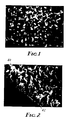
- a surface microlayer such as that depicted in Figs. 1 and 2 can be formed according to the following procedure.
- a clean metal substrate is prepared by either vacuum vapor depositing or ion sputter depositing a metal film onto a previously cleaned float glass slide. Suitable metals are those that are useful for preparing substrates, as noted previously. The thickness of the metal film is preferably on the order of 1000 Angstroms. Other materials useful for forming the substrate are bare float glass and standard laboratory microscope slides cleaned according to usual laboratory procedures.
- the substrate can be coated with the layer of organic material by depositing by means of physical vacuum vapor deposition, i.e. sublimation of the organic material under an applied vacuum.
- the temperature of the substrate during vapor deposition is not critical and the temperature range chosen can be varied, depending upon the organic material selected. For perylene red, a substrate temperature near room temperature (25°C) is satisfactory.
- the rate of vacuum vapor deposition can be varied. Thickness of the layer of organic material deposited can vary and the thickness chosen will determine the major dimension of the resultant microstructures after the annealing step is performed. Layer thicknesses in the range of 0.05 to 0.25 micrometers are generally preferred.
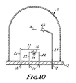
- FIG. 10 A typical apparatus for conducting vacuum vapor deposition is shown schematically in Fig. 10 and comprises a bell jar 10, a vacuum base plate 12 with ports 14, 16, 18 for rotary motion means 20, electrical power means 22, and water cooling means 24, respectively, quartz crystal thin film deposition monitor 26, a shutter 28 operated by the rotary motion means 20, a crucible 30 for the organic source material 32, a tungsten wire basket 34 for supporting and resistively heating the crucible 30.
- quartz crystal thin film deposition monitor 26 operated by the rotary motion means 20
- a crucible 30 for the organic source material 32 a tungsten wire basket 34 for supporting and resistively heating the crucible 30.
- Electrical power can be used to heat an alumina or quartz source crucible 30 containing the organic material 32 to be vapor deposited.
- the means for providing rotational motion 20 allows moving a shutter 28, so as to either interrupt or permit the deposition of the organic material 32 onto the substrate 36, which is mounted above the source crucible 30.
- the substrate 36 such as previously described, is placed in the vacuum bell jar 10 to which is attached a liquid nitrogen trapped, oil diffusion pump (not shown).
- the substrate 36 is positioned, metal side down, above the source crucible 30 within the bell jar 10.
- the distance from the substrate 36 to the source crucible 30 will affect the deposition rate and the film thickness. A typical distance is approximately 16.5 cm.
- the crucible 30 is first cleaned by heating it empty to glowing red temperatures under vacuum.
- the organic material 32 e.g. perylene red, is placed in the bottom of the crucible 30 to a depth of about 2 mm and gently tapped down to eliminate air pockets.
- the crucible 30 After evacuating the bell jar 10 to a pressure below 1 ⁇ 10 ⁇ 6 Torr, the crucible 30 is heated to 260°C for 30 minutes as a "pre-soak" to degas the organic material 32.
- a movable shutter 28 between the source crucible 30 and substrate 36 should remain closed during the pre-soak phase.
- the pre-soak step is then continued at about 285°C for an additional 45 minutes. During this time the system pressure is maintained at ca. 8 ⁇ 10 ⁇ 7 Torr. Heating current to the tungsten basket 34 holding the source crucible 30 is then increased to bring the crucible temperature to 380°C to 420°C. After 3 1/2 minutes, the shutter 28 is opened, allowing the organic material to sublime and deposit on the substrate.
- the deposition rate is greatest when the organic material 32 uniformly wets the interior of the crucible 30 and is prevented from forming an iris-like deposit on the top rim of the crucible by uniform heating.
- Deposition rates typically vary from 20 Angstroms per minute to 400 Angstroms per minutes and film thicknesses typically range from 500 to 2000 Angstroms, but these parameters can vary widely.
- no special means need be used to control the substrate temperature. It is typically found that the temperature of the metallized glass slide increases 10 to 15°C above ambient during vapor deposition.
- the rate of sublimation, and consequently, thickness of the organic film layer deposited on the substrate 36 can be determined by the use of a quartz crystal oscillator thin film deposition monitor 26.
- Such monitors are commercially available and are well known in the art.
- the coated substrate from the vapor deposition step is heated in a vacuum for a sufficient period of time such that the deposited film layer undergoes a physical change resulting in production of a microlayer comprising pure, single- or poly-crystalline microstructures. Exposure of the organic material coated substrate to the atmosphere before the annealing step is not detrimental to subsequent microstructure formation.
- the coated substrate can be heated by any suitable means (not shown) in a vacuum (not shown) of at least moderate quality, e.g., 1 ⁇ 10 ⁇ 3 Torr or lower, and in a temperature range of 160°C to 230°C.
- the time of annealing is dependent on the annealing temperature but a range of about 1/2 to about 6 hours, preferably about 1 1/2 to about 4 hours, is generally sufficient to convert the original organic film layer on the substrate to the microstructured film, as can be determined by scanning electron microscopy and reflection absorption infrared spectroscopy (see M. K. Debe, Appl. Surface Sci., 14 (1982-83) pp. 1-40).
- the interval between the vapor deposition step and the annealing step can vary from several minutes to several months, with no significant adverse effect, as long as the coated composite is stored in a covered container. However, the length of the interval is not critical.
- the annealing step can be monitored in situ with either an infrared spectroscopic technique (see Fig. 4), or the reflectance of a He-Ne laser beam at near grazing incidence. As the microstructures develop, the infrared band intensities change and the laser specular reflectivity drops, thus allowing the conversion to be carefully followed.
- the substrate is allowed to undergo a natural, unaided cooling before the vacuum chamber is backfilled with a gas (e.g., air) to attain atmospheric pressure and the substrate removed from the vacuum chamber.
- a gas e.g., air
- microstructured surfaces have required vacuum processes such as plasma, sputter, or reactive ion etching, or non-vacuum processes such as chemical etching, electro- or electroless deposition, anodizing, and etching for their production.
- vacuum processes such as plasma, sputter, or reactive ion etching, or non-vacuum processes such as chemical etching, electro- or electroless deposition, anodizing, and etching for their production.
- the composition of the microstructures heretofore were amorphous or polycrystalline oxides, alloys, or other polymeric forms which lacked the oriented, pure crystalline properties of the articles of this invention.
- inventions include articles that can be made by processes comprising additional coating of the articles obtained from the annealing step.
- Coating means that another material, organic, or inorganic, is either (a) put in intimate contact with the microstructures of the annealed article, or (b) applied as an overlayer to 'blanket' the annealed article.
- the coating can come in intimate contact with essentially the entire surface of the microstructure.
- this coating may or may not be a continuous film, depending on the microstructures and overall microlayer.
- the coating comes in contact primarily with the tips or distal ends of the microstructures so as to provide a continuous film.
- the successive overcoating of a previously coated article is also within the purview of this invention.
- the coating of the annealed article is preferably done by a vacuum deposition process to avoid the disturbance of the microstructures by mechanical-like forces of contact.
- This vacuum deposited coating can serve to strengthen the microlayer and permit further overcoating by means of the vacuum deposition technique described in this invention or by means of conventional coating techniques such as dipping, spraying, roll coating, knife, blade coating, and the like.
- Overcoating the coated and annealed articles with organic or inorganic materials can provide an overcoat as continuous or discontinuous films, depending upon the microlayer of the coated article.
- Marked changes in the resultant coated article can be noted.
- coating an annealed article with copper provides a black composite of low specular reflectivity and changed microlayer.
- Polyethylene overcoating of an annealed article, previously coated with copper provides a composite with secondary microtextured surface having different physical and chemical properties, the details of which are described in the examples.
- the articles of this invention are useful for many forms of light trapping, energy absorption, imaging, data transmission and storage and gradient index applications.
- the articles of this invention can be used to prepare photovoltaic devices, such as the type of device described in U.S. Patent 4,252,865, radiation absorbing devices, e.g. selective solar absorbers, flat plate solar collectors, solar absorption panels, such as the type of device described in U.S. Patent 4,148,294, solar cells, such as the type of device described in U.S. Patent 4,155,781, photo absorbing surfaces, such as the type of device described in U.S. Patent 4,209,008, optical storage media, such as the type of device described in "Textured surfaces: Optical Storage and Other Applications", H. G. Craighead, R. E. Howard, J. E. Sweeney, and D. M. Tennant, J. Vac. Sci. Technol., 20(3), March 1982.
- This example involves an article comprising an aluminum substrate that bears on the surface thereof a microlayer of perylene red.
- a substrate was formed by vacuum sputter depositing an aluminum film onto a 3 mm ⁇ 30 mm ⁇ 10 cm glass slide. The aluminum film was allowed to air oxidize by natural exposure to the atmosphere. Then, the aluminum coated glass slide was installed in a vacuum bell jar to which was attached a liquid nitrogen trap and diffusion pump capable of attaining vacuums in the range of about 1 ⁇ 10 ⁇ 7 Torr.
- Approximately 0.1 gram of commercially available perylene red was placed in an alumina crucible, which was in turn heated by a tungsten basket heater in the vacuum bell jar.
- the perylene red was vacuum purified by degassing it during a "pre-soak" heating period, during which time the crucible was maintained at 260°C to 385°C for over 2 hours.
- the electrical power applied to the crucible heating basket was increased to cause the interior crucible temperature to exceed 380°C, thus initiating sublimation of the perylene red.
- the sublimation rate of the perylene red was monitored with a quartz crystal oscillator thin film deposition monitor.
- the shutter was opened to allow the perylene red vapor to deposit on the surface of the aluminum substrate and thin film monitor.
- the perylene red film was allowed to form on the aluminum substrate to a total thickness of 0.15 micrometers before the shutter was closed.
- the aluminized substrate temperature was not actively controlled but varied between 25° to 40°C.
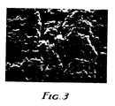
- Fig. 3 shows an SEM micrograph of a rough portion of the as-deposited film, which, after the annealing step resulted in the microstructured surface (see Figs. 1 and 2).
- the aluminized glass composite, bearing a 1500 Angstrom thick film of perylene red, was removed from the bell jar system, and inserted into a second similar vacuum bell jar equipped with a heater assembly capable of heating the entire continuous perylene red-coated surface of the composite by thermal conduction through the 3 mm thick glass substrate.
- the perylene red composite was heated at approximately 190°C over a period of several hours while the annealing step was continuously monitored, with the technique of reflection absorption infrared spectroscopy (RAIR) to measure the phase transition growth of the microstructures.
- Fig. 4 shows the observed infrared spectral changes that occurred in the composite before and after the formation of microstructures. The significant relative band intensity changes are indicative of the occurrence of preferential orienting of perylene red molecules relative to the aluminum substrate.
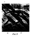
- Microstructures 40 are seen to be about 1.5 micrometers in length, oriented substantially perpendicular to the aluminum film substrate 42, and, as may be deduced from inspection of Fig. 1, have areal number densities on the order of 50 per square micrometer. Microstructures 40 appear to have uniform cross-sectional dimensions along their lengths, and though touching at times at their bases, are essentially discrete and non-contacting. While they appear to have a round cross-section in Figs. 1 and 2, due to limited resolution of the SEM, the microstructures actually are lath shaped, as shown in Fig. 5. Microstructures 44 in the TEM image are seen to have very straight sides and are exceptionally uniform in cross-section along their lengths.
- the pattern of dots 46 are clusters of platinum microislands that were vapor deposited onto the microstructures after the latter were mechanically removed from the substrate by rubbing and transferred to a Formvar® brand polyvinylformaldehyde plastic coated TEM sample grid.
- the platinum preferentially nucleates at defect sites on the surfaces of the microstructures and very clearly delineates the presence of step edges 48 running parallel to the major dimension the microstructures (see Fig. 5), indicating a high degree of crystalline perfection along the entire length of the microstructure.
- Microstructures of perylene red produced by the process of this invention are single- or polycrystalline, have a cubic lattice structure and [211] growth axis standing substantially normal to the surface of the substrate.
- Cross-sectional dimensions of perylene red microstructures are uniform along their lengths and display a narrow size distribution from microstructure to microstructure.
- the width of perylene red microstructures is 0.052 micrometers on average and their thickness is 0.027 micrometers on average.
- Side planes of perylene red microstructures have (001) and (111) crystal indices.
- the individual, oriented microstructures are discrete, essentially non-touching at their base (i.e., the point of contact of the microstructure with the substrate), and are densely arrayed with mean spacings on the order of 0.05 micrometers, giving areal number densities of about 5 billion microelements per square centimeter or 50 microelements per square micrometer.
- Average length of the microstructures depends on the initial uniform film thickness, and is approximately 10 to 15 times this initial value. Aspect ratios are typically in the range of 10 to 80 for the initial thickness range above and an order of magnitude increase in specific surface area.
- This example involves another embodiment of this invention, wherein the microlayer of a microstructured article made according to the method of Example 1 was coated with copper metal.
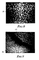
- a mass equivalent of 500 Angstroms of copper was ion sputter deposited onto the microstructures 50 of the article made according to Example 1 (see Fig. 6); this amount was increased to 1000 Angstroms for microstructures 52 (see Fig. 7) and 2000 Angstroms for microstructures 54 (see Fig. 8).
- Metal coated microstructures 50 provide a very efficient light trapping surface and accordingly appear very black.
- the metal coated microstructures 52 and 54 caused the surface to appear dark gray and light gray respectively, and provided the surface with an extraordinarily low specular reflectivity.
- the microlayer scale was seen to change as the dimensions of the microstructures changed because of the epitaxial metal growth on the sides of the microstructures.
- This example involves another embodiment of this invention wherein a 500 Angstrom coating of copper metal, which had been previously sputter-coated onto a microstructured article made according to Example 1, is overcoated with a film of polyethylene by means of vacuum vapor deposition (see Fig. 9).
- the polyethylene was deposited onto the copper coated article to a thickness substantially greater than the length of the major dimension of the microstructures 56, so as to generate a new microtextured surface of much larger scale and different chemical nature.
- the polymer overcoating may also serve as a protective coating for the underlying microstructured surface.
- This example involves an article having copper deposited as a coating onto a microstructured article made according to Example 1, wherein a platinum substrate had first been deposited onto a glass slide by vapor deposition.
- Example 2 As described in Example 1, a glass slide sputter coated with platinum, was coated by means of vapor deposition with perylene red to a thickness of 1650 Angstroms at a mean deposition rate of 410 Angstroms per minute.
- the annealing step was carried out by heating the sample at gradually incremented temperatures in the range of ca. 165 to 205°C.
- the annealing step was monitored with IR spectroscopy until the band intensities became constant with time, i.e. stabilized.
- Metal coated microstructures of this invention had an extremely low specular reflectivity.
- the specular reflectivity of the sample region having 1000 Angstrom thick layer of copper was measured at 7.5° off normal incidence and found to be less than 1.5% between wavelengths of 2500 nm and 2000 nm, and below 0.5% between wavelengths of 2000 nm and 185 nm, relative to an aluminum reference mirror.
- This ability to go from a surface characterizable as having low specular and low diffuse reflectivity to one of low specular and high diffuse reflectivity by simply doubling the thickness of metal coating on the microstructures is considered an important aspect of this invention.
- the metal-coated article prepared in Example 2 was overcoated, by vacuum vapor coating, with a non-conductive, polymeric material, namely polyethylene.
- a non-conductive, polymeric material namely polyethylene.
- Commercially available polyethylene pellets were inserted into a quartz tube, approximately 13.3 cm (5.25 inches) long and 0.95 cm (0.375 inches) in diameter, having a 0.16 cm by 8.26 cm slot cut longitudinally on one side of the tube.
- the tube was placed in a vacuum bell jar and heated by passing current through a nichrome film previously sputter coated on the outside surface of the quartz tube. The ends of the quartz tube were blocked with quartz plugs.
- the slot was oriented upward in the vacuum bell jar and parallel to the long axis of the metal-coated microstructured article, which was positioned approximately 3.8 cm. (1.5 inches) above the quartz tube.
- the quartz tube was heated by dissipating ca. 9 watts of power for 16 minutes in the nichrome film, which caused a film of polyethylene to be vapor coated onto the metal coated microstructures of the composite.
- Fig. 9 shows an SEM micrograph of the sample, at a point where the overcoated polyethylene 58 was stripped away, revealing the underlying metal coated microstructures 56 in a region where 500 Angstrom thick layer of copper had been deposited.
- a SEM micrograph of the underside of the stripped away polyethylene overlayer revealed a multiplicity of hemispherical depressions where the distal ends (rounded 'heads') of the copper-coated microstructures had been partially embedded in the polyethylene overlayer.
- the visual effect of the polyethylene was to reduce even further the specular and diffuse reflectivity of the surface.
- the region with the 1000 Angstrom thick layer of copper and polymeric coating, discussed in Example 4 above was now measured to have a specular reflectivity at 7.5° off normal incidence of only 0.9% at a wavelength of 2500 nm, reducing to 0.1% at wavelengths between 2000 nm and 900 nm, and 0.3% at a wavelength of 850 nm.
- This example demonstrates generation of a microlayer wherein the organic material is a porphyrin.
- Metal-free phthalocyanine was deposited onto an aluminized glass substrate, according to procedure of Example 1.
- the thickness of the organic layer was 500 Angstroms, the deposition rate was 45 Angstroms per minute, and the background pressure was ca. 2 ⁇ 10 ⁇ 6 Torr.
- the resulting composite was installed into a second vacuum chamber and annealed at a pressure of 4 ⁇ 10 ⁇ 8Torr by gradually increasing the film temperature in steps to a maximum of approximaely 190°C over a period of 2 1/2 hours. Heating was stopped when the maximum temperature was reached. Scanning electron micrographs of the resulting surface showed an array of crystalline, whisker-shaped microstructures, having a uniform cross-section, approximately square-shaped, each side of the square being approximately 500 Angstroms.
- microstructures were oriented essentially perpendicular to the surface of the substrate, and they had an aspect ratio in the range of 5 to 10.
- the number of microstructures per unit area was not as high as that for the perylene red material in the previous examples, probably due to premature stoppage of the annealing.
- a second sample of the same organic material was deposited and annealed in the same manner as was the first sample, the only differences being that the layer of organic material was 900 Angstroms thick, and the annealing was maintained above ca 180°C to 200°C for over two hours. During the two hour period at elevated temperature, some of the material desorbed, but the material remaining on the cooler edges of the sample displayed the same oriented crystalline microstructures as seen on the previously described 500 Angstrom sample. The microstructures were slightly longer and the areal number density was slightly higher, being about 5 microstructures per square micrometer.
Landscapes
- Chemical & Material Sciences (AREA)
- Engineering & Computer Science (AREA)
- Materials Engineering (AREA)
- Metallurgy (AREA)
- Organic Chemistry (AREA)
- Mechanical Engineering (AREA)
- Chemical Kinetics & Catalysis (AREA)
- Crystallography & Structural Chemistry (AREA)
- Physics & Mathematics (AREA)
- Thermal Sciences (AREA)
- Sustainable Development (AREA)
- Life Sciences & Earth Sciences (AREA)
- Sustainable Energy (AREA)
- Combustion & Propulsion (AREA)
- General Engineering & Computer Science (AREA)
- General Chemical & Material Sciences (AREA)
- Spectroscopy & Molecular Physics (AREA)
- Laminated Bodies (AREA)
- Physical Vapour Deposition (AREA)
- Application Of Or Painting With Fluid Materials (AREA)
- Crystals, And After-Treatments Of Crystals (AREA)
- Mechanical Treatment Of Semiconductor (AREA)
- Addition Polymer Or Copolymer, Post-Treatments, Or Chemical Modifications (AREA)
- Polishing Bodies And Polishing Tools (AREA)
- Manufacture Of Macromolecular Shaped Articles (AREA)
Priority Applications (1)
| Application Number | Priority Date | Filing Date | Title |
|---|---|---|---|
| AT87112108T ATE92977T1 (de) | 1986-08-25 | 1987-08-20 | Anordnung mit einer oberflaechenschicht, die gleichmaessig orientierte, kristalline, organische mikrostrukturen enthaelt. |
Applications Claiming Priority (2)
| Application Number | Priority Date | Filing Date | Title |
|---|---|---|---|
| US06/899,653 US4812352A (en) | 1986-08-25 | 1986-08-25 | Article having surface layer of uniformly oriented, crystalline, organic microstructures |
| US899653 | 1986-08-25 |
Publications (3)
| Publication Number | Publication Date |
|---|---|
| EP0258752A2 true EP0258752A2 (de) | 1988-03-09 |
| EP0258752A3 EP0258752A3 (en) | 1989-12-06 |
| EP0258752B1 EP0258752B1 (de) | 1993-08-11 |
Family
ID=25411344
Family Applications (1)
| Application Number | Title | Priority Date | Filing Date |
|---|---|---|---|
| EP19870112108 Expired - Lifetime EP0258752B1 (de) | 1986-08-25 | 1987-08-20 | Anordnung mit einer Oberflächenschicht, die gleichmässig orientierte, kristalline, organische Mikrostrukturen enthält |
Country Status (7)
| Country | Link |
|---|---|
| US (1) | US4812352A (de) |
| EP (1) | EP0258752B1 (de) |
| JP (1) | JP2579950B2 (de) |
| AT (1) | ATE92977T1 (de) |
| CA (1) | CA1328784C (de) |
| DE (1) | DE3786964T2 (de) |
| HK (1) | HK1007574A1 (de) |
Cited By (3)
| Publication number | Priority date | Publication date | Assignee | Title |
|---|---|---|---|---|
| EP0352931A1 (de) * | 1988-07-13 | 1990-01-31 | Minnesota Mining And Manufacturing Company | Organische dünne Schicht durch regulierbare Molekularepitaxie |
| WO1993000560A1 (en) * | 1991-06-24 | 1993-01-07 | Minnesota Mining And Manufacturing Company | Composite article comprising oriented microstructures |
| US6630128B1 (en) | 1998-08-28 | 2003-10-07 | Destiny Pharma Limited | Porphyrin derivatives their use in photodynamic therapy and medical devices containing them |
Families Citing this family (111)
| Publication number | Priority date | Publication date | Assignee | Title |
|---|---|---|---|---|
| GB2224040B (en) * | 1988-08-29 | 1992-09-30 | Minnesota Mining & Mfg | Array of densely packed discrete metal microspheres |
| US5063538A (en) * | 1989-08-30 | 1991-11-05 | Kuehnle Manfred R | Optoelectronic signal recording medium and method of making same |
| US5238729A (en) * | 1991-04-05 | 1993-08-24 | Minnesota Mining And Manufacturing Company | Sensors based on nanosstructured composite films |
| US5327373A (en) * | 1992-08-21 | 1994-07-05 | Board Of Regents, The University Of Texas System | Optoelectronic memories with photoconductive thin films |
| US5352651A (en) * | 1992-12-23 | 1994-10-04 | Minnesota Mining And Manufacturing Company | Nanostructured imaging transfer element |
| US5338430A (en) * | 1992-12-23 | 1994-08-16 | Minnesota Mining And Manufacturing Company | Nanostructured electrode membranes |
| US5326619A (en) * | 1993-10-28 | 1994-07-05 | Minnesota Mining And Manufacturing Company | Thermal transfer donor element comprising a substrate having a microstructured surface |
| US5459016A (en) * | 1993-12-16 | 1995-10-17 | Minnesota Mining And Manufacturing Company | Nanostructured thermal transfer donor element |
| US5659296A (en) * | 1994-10-24 | 1997-08-19 | Minnesota Mining And Manufacturing Company | Exposure indicating apparatus |
| US5666949A (en) * | 1994-10-24 | 1997-09-16 | Minnesota Mining And Manufacturing Company | Exposure indicator with continuous alarm signal indicating multiple conditions |
| US5709943A (en) * | 1995-05-04 | 1998-01-20 | Minnesota Mining And Manufacturing Company | Biological adsorption supports |
| US5674592A (en) * | 1995-05-04 | 1997-10-07 | Minnesota Mining And Manufacturing Company | Functionalized nanostructured films |
| DE69522815T2 (de) * | 1995-07-24 | 2002-04-11 | International Business Machines Corp., Armonk | Epitaxie-schichtstruktur |
| US5726524A (en) * | 1996-05-31 | 1998-03-10 | Minnesota Mining And Manufacturing Company | Field emission device having nanostructured emitters |
| DE69839010T2 (de) * | 1997-04-29 | 2009-01-02 | Ciba Holding Inc. | Beschreibbare und löschbare optische aufzeichnungsmedien mit hoher dichte |
| US6042959A (en) | 1997-10-10 | 2000-03-28 | 3M Innovative Properties Company | Membrane electrode assembly and method of its manufacture |
| US5879827A (en) * | 1997-10-10 | 1999-03-09 | Minnesota Mining And Manufacturing Company | Catalyst for membrane electrode assembly and method of making |
| US6136412A (en) * | 1997-10-10 | 2000-10-24 | 3M Innovative Properties Company | Microtextured catalyst transfer substrate |
| US5879828A (en) * | 1997-10-10 | 1999-03-09 | Minnesota Mining And Manufacturing Company | Membrane electrode assembly |
| US5910378A (en) | 1997-10-10 | 1999-06-08 | Minnesota Mining And Manufacturing Company | Membrane electrode assemblies |
| JP2002529892A (ja) | 1998-10-29 | 2002-09-10 | スリーエム イノベイティブ プロパティズ カンパニー | 微細構造化流れ場 |
| US6238534B1 (en) | 1999-05-14 | 2001-05-29 | 3M Innovative Properties Company | Hybrid membrane electrode assembly |
| US6521324B1 (en) | 1999-11-30 | 2003-02-18 | 3M Innovative Properties Company | Thermal transfer of microstructured layers |
| US6646075B2 (en) | 1999-12-23 | 2003-11-11 | 3M Innovative Properties Company | High molecular weight perfluorocyclobutane polymers and method of making |
| US6482763B2 (en) | 1999-12-29 | 2002-11-19 | 3M Innovative Properties Company | Suboxide fuel cell catalyst for enhanced reformate tolerance |
| US6559237B1 (en) | 2000-06-05 | 2003-05-06 | 3M Innovative Properties Company | Sulfonated perfluorocyclobutane ion-conducting membranes |
| US6268532B1 (en) | 2000-06-05 | 2001-07-31 | 3M Innovative Properties Company | Sulfonated perfluorovinyl functional monomers |
| US6555213B1 (en) | 2000-06-09 | 2003-04-29 | 3M Innovative Properties Company | Polypropylene card construction |
| US6506478B1 (en) | 2000-06-09 | 2003-01-14 | 3M Innovative Properties Company | Inkjet printable media |
| US6979480B1 (en) * | 2000-06-09 | 2005-12-27 | 3M Innovative Properties Company | Porous inkjet receptor media |
| AU2001222589A1 (en) | 2000-06-09 | 2001-12-24 | 3M Innovative Properties Company | Materials and methods for creating waterproof, durable aqueous inkjet receptive media |
| JP2002146516A (ja) * | 2000-11-07 | 2002-05-22 | Sony Corp | 有機薄膜の蒸着方法 |
| US6969897B2 (en) * | 2002-12-10 | 2005-11-29 | Kim Ii John | Optoelectronic devices employing fibers for light collection and emission |
| US7972616B2 (en) * | 2003-04-17 | 2011-07-05 | Nanosys, Inc. | Medical device applications of nanostructured surfaces |
| US20050038498A1 (en) * | 2003-04-17 | 2005-02-17 | Nanosys, Inc. | Medical device applications of nanostructured surfaces |
| US20050112450A1 (en) * | 2003-09-08 | 2005-05-26 | Intematix Corporation | Low platinum fuel cell catalysts and method for preparing the same |
| US8211593B2 (en) * | 2003-09-08 | 2012-07-03 | Intematix Corporation | Low platinum fuel cells, catalysts, and method for preparing the same |
| US7351444B2 (en) * | 2003-09-08 | 2008-04-01 | Intematix Corporation | Low platinum fuel cell catalysts and method for preparing the same |
| US7419741B2 (en) * | 2003-09-29 | 2008-09-02 | 3M Innovative Properties Company | Fuel cell cathode catalyst |
| WO2005116695A1 (en) * | 2004-05-27 | 2005-12-08 | Matsushita Electric Industrial Co., Ltd. | Light-absorbing member |
| JP4506326B2 (ja) * | 2004-07-21 | 2010-07-21 | 凸版印刷株式会社 | バリア性容器 |
| US7572534B2 (en) * | 2004-09-20 | 2009-08-11 | 3M Innovative Properties Company | Fuel cell membrane electrode assembly |
| US8101317B2 (en) * | 2004-09-20 | 2012-01-24 | 3M Innovative Properties Company | Durable fuel cell having polymer electrolyte membrane comprising manganese oxide |
| US20060147791A1 (en) * | 2004-12-30 | 2006-07-06 | Debe Mark K | Platinum recovery from fuel cell stacks |
| US20060144791A1 (en) * | 2004-12-30 | 2006-07-06 | Debe Mark K | Platinum recovery from nanostructured fuel cell catalyst |
| CA2597290A1 (en) * | 2005-02-16 | 2006-08-24 | 3M Innovative Properties Company | Fuel cell catalyst |
| US20080020923A1 (en) * | 2005-09-13 | 2008-01-24 | Debe Mark K | Multilayered nanostructured films |
| US20070059452A1 (en) * | 2005-09-13 | 2007-03-15 | Debe Mark K | Formation of nanostructured layers through continued screw dislocation growth |
| US7790304B2 (en) * | 2005-09-13 | 2010-09-07 | 3M Innovative Properties Company | Catalyst layers to enhance uniformity of current density in membrane electrode assemblies |
| US7622217B2 (en) * | 2005-10-12 | 2009-11-24 | 3M Innovative Properties Company | Fuel cell nanocatalyst |
| US20070082814A1 (en) * | 2005-10-12 | 2007-04-12 | 3M Innovative Properties Company | Ternary nanocatalyst and method of making |
| US8628871B2 (en) | 2005-10-28 | 2014-01-14 | 3M Innovative Properties Company | High durability fuel cell components with cerium salt additives |
| US8367267B2 (en) * | 2005-10-28 | 2013-02-05 | 3M Innovative Properties Company | High durability fuel cell components with cerium oxide additives |
| US7740902B2 (en) * | 2006-04-20 | 2010-06-22 | 3M Innovative Properties Company | Method for making oxygen-reducing catalyst layers |
| US7906251B2 (en) * | 2006-04-20 | 2011-03-15 | 3M Innovative Properties Company | Oxygen-reducing catalyst layer |
| US8288059B2 (en) | 2006-12-15 | 2012-10-16 | 3M Innovative Properties Company | Processing methods and systems for assembling fuel cell perimeter gaskets |
| US8012284B2 (en) * | 2006-12-15 | 2011-09-06 | 3M Innovative Properties Company | Method and apparatus for fabricating roll good fuel cell subassemblies |
| US7732083B2 (en) * | 2006-12-15 | 2010-06-08 | 3M Innovative Properties Company | Gas diffusion layer incorporating a gasket |
| ATE524843T1 (de) | 2007-04-12 | 2011-09-15 | 3M Innovative Properties Co | Leistungsstarke und langlebige nichtedelmetall- brennstoffzellenkatalysatoren |
| US20090041986A1 (en) * | 2007-06-21 | 2009-02-12 | 3M Innovative Properties Company | Method of making hierarchical articles |
| US20080315459A1 (en) * | 2007-06-21 | 2008-12-25 | 3M Innovative Properties Company | Articles and methods for replication of microstructures and nanofeatures |
| US20090114618A1 (en) * | 2007-06-21 | 2009-05-07 | 3M Innovative Properties Company | Method of making hierarchical articles |
| US8426078B2 (en) * | 2007-12-21 | 2013-04-23 | 3M Innovative Properties Company | Manufacturing of fuel cell membrane electrode assemblies incorporating photocurable cationic crosslinkable resin gasket |
| JP5196988B2 (ja) * | 2007-12-21 | 2013-05-15 | スリーエム イノベイティブ プロパティズ カンパニー | インク組成物、その製造方法、そのインク組成物を用いて形成した電極触媒層及びこれらの用途 |
| US20100035124A1 (en) * | 2008-08-11 | 2010-02-11 | Gm Clobal Technology Operations, Inc. | Hybrid particle and core-shell electrode structure |
| JP5580312B2 (ja) * | 2008-08-25 | 2014-08-27 | スリーエム イノベイティブ プロパティズ カンパニー | 電圧反転耐性を有する燃料電池用ナノ触媒 |
| EP2423714A4 (de) * | 2009-04-24 | 2018-05-02 | Sharp Kabushiki Kaisha | Antireflexionsfilm, verfahren zur herstellung des antireflexionsfilms und anzeigevorrichtung |
| US8512908B2 (en) * | 2009-05-14 | 2013-08-20 | GM Global Technology Operations LLC | Fabrication of catalyst coated diffusion media layers containing nanostructured thin catalytic layers |
| US8802329B2 (en) | 2009-05-14 | 2014-08-12 | GM Global Technology Operations LLC | Electrode containing nanostructured thin catalytic layers and method of making |
| US8507152B2 (en) * | 2009-05-14 | 2013-08-13 | GM Global Technology Operations LLC | Fabrication of electrodes with multiple nanostructured thin catalytic layers |
| US8481231B2 (en) * | 2009-05-14 | 2013-07-09 | GM Global Technology Operations LLC | Preparation of nanostructured thin catalytic layer-based electrode ink |
| WO2010143503A1 (ja) | 2009-06-12 | 2010-12-16 | シャープ株式会社 | 反射防止膜、表示装置及び透光部材 |
| JP6001455B2 (ja) * | 2009-12-22 | 2016-10-05 | スリーエム イノベイティブ プロパティズ カンパニー | ナノ構造触媒及び分散した触媒副層を有する燃料電池電極 |
| JP5973423B2 (ja) | 2010-04-26 | 2016-08-23 | スリーエム イノベイティブ プロパティズ カンパニー | アニーリングされたナノ構造薄膜触媒 |
| WO2011139693A2 (en) | 2010-04-26 | 2011-11-10 | 3M Innovative Properties Company | Platinum nickel catalyst alloy |
| WO2011139678A1 (en) | 2010-04-26 | 2011-11-10 | 3M Innovative Properties Company | Fuel cell water management via reduced anode reactant pressure |
| US8445164B2 (en) | 2010-05-27 | 2013-05-21 | GM Global Technology Operations LLC | Electrode containing nanostructured thin catalytic layers and method of making |
| US9085019B2 (en) | 2010-10-28 | 2015-07-21 | 3M Innovative Properties Company | Superhydrophobic films |
| US8796170B2 (en) | 2011-02-04 | 2014-08-05 | Ford Global Technologies, Llc | Layered catalyst |
| CN103857831B (zh) | 2011-10-10 | 2016-08-17 | 3M创新有限公司 | 催化剂电极及其制备和使用方法 |
| CN104081570A (zh) | 2011-12-29 | 2014-10-01 | 3M创新有限公司 | 电化学电池电极 |
| US8518596B1 (en) | 2012-05-16 | 2013-08-27 | GM Global Technology Operations LLC | Low cost fuel cell diffusion layer configured for optimized anode water management |
| US9153822B2 (en) | 2012-08-14 | 2015-10-06 | Ford Global Technologies, Llc | Nano-structured thin film catalyst |
| WO2014099790A1 (en) | 2012-12-19 | 2014-06-26 | 3M Innovative Properties Company | Nanostructured whisker article |
| CA2909743A1 (en) | 2013-04-23 | 2014-11-27 | 3M Innovative Properties Company | Catalyst electrodes and method of making it |
| KR20170095296A (ko) | 2014-12-15 | 2017-08-22 | 쓰리엠 이노베이티브 프로퍼티즈 캄파니 | 막 전극 접합체 |
| US11094953B2 (en) | 2015-05-26 | 2021-08-17 | 3M Innovative Properties Company | Electrode membrane assembly having an oxygen evolution catalyst electrodes, and methods of making and using the same |
| JP6488928B2 (ja) * | 2015-07-15 | 2019-03-27 | アイシン精機株式会社 | 蒸着装置 |
| JP7076715B2 (ja) | 2016-10-26 | 2022-05-30 | スリーエム イノベイティブ プロパティズ カンパニー | 触媒 |
| CN109891647A (zh) | 2016-10-26 | 2019-06-14 | 3M创新有限公司 | 用于燃料电池的pt-ni-ir催化剂 |
| EP3533099B1 (de) | 2016-10-26 | 2020-11-25 | 3M Innovative Properties Company | Pt-ni-ir katalysator für brennstoffzelle |
| KR20190069523A (ko) | 2016-10-26 | 2019-06-19 | 쓰리엠 이노베이티브 프로퍼티즈 캄파니 | 촉매 |
| WO2018118877A1 (en) | 2016-12-20 | 2018-06-28 | 3M Innovative Properties Company | Electrolyzer including a porous hydrophobic gas diffusion layer |
| JP6809897B2 (ja) | 2016-12-20 | 2021-01-06 | スリーエム イノベイティブ プロパティズ カンパニー | 膜電極接合体及び固体高分子形燃料電池 |
| WO2018185616A1 (en) | 2017-04-03 | 2018-10-11 | 3M Innovative Properties Company | Water electrolyzers |
| EP3607114A1 (de) | 2017-04-03 | 2020-02-12 | 3M Innovative Properties Company | Wasserelektrolysatoren |
| EP3607113B1 (de) | 2017-04-03 | 2023-07-19 | 3M Innovative Properties Company | Wasserelektrolysatoren |
| EP3728684A4 (de) | 2017-12-22 | 2021-09-22 | 3M Innovative Properties Company | Dispergierte katalysatorhaltige anodenzusammensetzungen für elektrolysatoren |
| CN112243541A (zh) | 2018-04-04 | 2021-01-19 | 3M创新有限公司 | 催化剂 |
| WO2019193461A1 (en) | 2018-04-04 | 2019-10-10 | 3M Innovative Properties Company | Catalyst comprising pt, ni, and cr |
| US20210013521A1 (en) | 2018-04-04 | 2021-01-14 | 3M Innovative Properties Company | Catalyst comprising pt, ni, and ta |
| US20210008528A1 (en) | 2018-04-04 | 2021-01-14 | 3M Innovative Properties Company | Catalyst comprising pt, ni, and ru |
| US11955645B2 (en) | 2018-04-13 | 2024-04-09 | 3M Innovative Properties Company | Catalyst |
| WO2019198033A1 (en) | 2018-04-13 | 2019-10-17 | 3M Innovative Properties Company | Catalyst |
| US11476470B2 (en) | 2018-04-13 | 2022-10-18 | 3M Innovative Properties Company | Catalyst |
| US20210242480A1 (en) | 2018-05-01 | 2021-08-05 | 3M Innovative Properties Company | Platinum-coated polyimide particles and articles thereof |
| DE102018116373A1 (de) | 2018-07-06 | 2020-01-09 | Schaeffler Technologies AG & Co. KG | Katalysatoranordnung für ein Elektrolyseursystem oder ein Brennstoffzellensystem, Elektrolyseursystem, Brennstoffzellensystem, Verwendung einer Katalysatoranordnung und Verfahren zur Herstellung einer Katalysatoranordnung |
| US11560632B2 (en) | 2018-09-27 | 2023-01-24 | 3M Innovative Properties Company | Membrane, membrane electrode assembly, and water electrolyzer including the same |
| WO2020121079A1 (en) | 2018-12-13 | 2020-06-18 | 3M Innovative Properties Company | Catalyst |
| JP2022514560A (ja) | 2018-12-19 | 2022-02-14 | スリーエム イノベイティブ プロパティズ カンパニー | 水電解装置 |
| CN112610608B (zh) * | 2020-11-26 | 2022-07-15 | 东南大学 | 一种宽温域自润滑轴承及其制备方法 |
Family Cites Families (15)
| Publication number | Priority date | Publication date | Assignee | Title |
|---|---|---|---|---|
| US3862127A (en) * | 1968-08-30 | 1975-01-21 | Xerox Corp | Process |
| US3932180A (en) * | 1973-06-04 | 1976-01-13 | Xerox Corporation | Direct alpha to X phase conversion of metal-free phthalocyanine |
| DE2616662C2 (de) * | 1976-04-15 | 1984-02-02 | Dornier System Gmbh, 7990 Friedrichshafen | Verfahren zur herstellung einer selektiven solarabsorberschicht auf aluminium |
| US4155781A (en) * | 1976-09-03 | 1979-05-22 | Siemens Aktiengesellschaft | Method of manufacturing solar cells, utilizing single-crystal whisker growth |
| US4252843A (en) * | 1977-02-18 | 1981-02-24 | Minnesota Mining And Manufacturing Company | Process for forming a microstructured transmission and reflectance modifying coating |
| US4190321A (en) * | 1977-02-18 | 1980-02-26 | Minnesota Mining And Manufacturing Company | Microstructured transmission and reflectance modifying coating |
| US4123267A (en) * | 1977-06-27 | 1978-10-31 | Minnesota Mining And Manufacturing Company | Photoconductive element having a barrier layer of aluminum hydroxyoxide |
| US4209008A (en) * | 1977-07-26 | 1980-06-24 | United Technologies Corporation | Photon absorbing surfaces and methods for producing the same |
| US4252865A (en) * | 1978-05-24 | 1981-02-24 | National Patent Development Corporation | Highly solar-energy absorbing device and method of making the same |
| US4340276A (en) * | 1978-11-01 | 1982-07-20 | Minnesota Mining And Manufacturing Company | Method of producing a microstructured surface and the article produced thereby |
| US4396643A (en) * | 1981-06-29 | 1983-08-02 | Minnesota Mining And Manufacturing Company | Radiation absorbing surfaces |
| US4563301A (en) * | 1982-12-13 | 1986-01-07 | Northwestern University | Electrically conductive low dimensional organomacrocycle compositions, articles and fabrication methods |
| US4563300A (en) * | 1982-12-20 | 1986-01-07 | Northwestern University | Electrically conductive cofacially crystallizing organomacrocycle compositions, articles and fabrication methods |
| JPS60162201A (ja) * | 1984-02-01 | 1985-08-24 | Mita Ind Co Ltd | 反射板 |
| JPH11752A (ja) * | 1997-06-10 | 1999-01-06 | Ueda Shokai Kk | 球形インゴット及び該インゴットの炉への投入装置 |
-
1986
- 1986-08-25 US US06/899,653 patent/US4812352A/en not_active Expired - Lifetime
-
1987
- 1987-07-17 CA CA 542368 patent/CA1328784C/en not_active Expired - Fee Related
- 1987-08-20 EP EP19870112108 patent/EP0258752B1/de not_active Expired - Lifetime
- 1987-08-20 AT AT87112108T patent/ATE92977T1/de not_active IP Right Cessation
- 1987-08-20 DE DE87112108T patent/DE3786964T2/de not_active Expired - Lifetime
- 1987-08-24 JP JP21002587A patent/JP2579950B2/ja not_active Expired - Lifetime
-
1998
- 1998-06-25 HK HK98106770A patent/HK1007574A1/en not_active IP Right Cessation
Cited By (3)
| Publication number | Priority date | Publication date | Assignee | Title |
|---|---|---|---|---|
| EP0352931A1 (de) * | 1988-07-13 | 1990-01-31 | Minnesota Mining And Manufacturing Company | Organische dünne Schicht durch regulierbare Molekularepitaxie |
| WO1993000560A1 (en) * | 1991-06-24 | 1993-01-07 | Minnesota Mining And Manufacturing Company | Composite article comprising oriented microstructures |
| US6630128B1 (en) | 1998-08-28 | 2003-10-07 | Destiny Pharma Limited | Porphyrin derivatives their use in photodynamic therapy and medical devices containing them |
Also Published As
| Publication number | Publication date |
|---|---|
| DE3786964D1 (de) | 1993-09-16 |
| EP0258752A3 (en) | 1989-12-06 |
| CA1328784C (en) | 1994-04-26 |
| EP0258752B1 (de) | 1993-08-11 |
| US4812352A (en) | 1989-03-14 |
| DE3786964T2 (de) | 1994-04-07 |
| ATE92977T1 (de) | 1993-08-15 |
| JP2579950B2 (ja) | 1997-02-12 |
| HK1007574A1 (en) | 1999-04-16 |
| JPS63107548A (ja) | 1988-05-12 |
Similar Documents
| Publication | Publication Date | Title |
|---|---|---|
| US4812352A (en) | Article having surface layer of uniformly oriented, crystalline, organic microstructures | |
| US5039561A (en) | Method for preparing an article having surface layer of uniformly oriented, crystalline, organic microstructures | |
| HK1007574B (en) | Article having surface layer of uniformly oriented, crystalline, organic microstructures | |
| US4252865A (en) | Highly solar-energy absorbing device and method of making the same | |
| Menadue | Si (111) surface structures by glancing-incidence high-energy electron diffraction | |
| EP0591375B1 (de) | Verbundartikel mit orientierten Mikrostrukturen und Verfahren zu dessen Herstellung | |
| US5176786A (en) | Organic thin film controlled molecular epitaxy | |
| US4940854A (en) | Organic thin film controlled molecular epitaxy | |
| Ow-Yang et al. | A time-resolved reflectivity study of the amorphous-to-crystalline transformation kinetics in dc-magnetron sputtered indium tin oxide | |
| CA1167718A (en) | Light-absorbing materials | |
| Harding et al. | Sputter etched metal solar selective absorbing surfaces for high temperature thermal collectors | |
| Gilbert et al. | Black germanium solar selective absorber surfaces | |
| Hussain et al. | Structure and morphology of laser-ablated WO3 thin films | |
| Kolesar Jr et al. | Optical reflectance reduction of textured silicon surfaces coated with an antireflective thin film | |
| Harding | Evaporated chromium black selective solar absorbers | |
| Kolesar Jr et al. | Mid-infrared (2.5≤ λ≤ 12.5 μm) optical absorption enhancement of textured silicon surfaces coated with an antireflective thin film | |
| Cocks et al. | The dependence of the texture of tellurium thin films on vacuum deposition angle | |
| Soltane et al. | Structural, morphological, and optical properties of AgxO thin films deposited via obliquely angle deposition | |
| Peterson et al. | The preparation of textured Te thin films with pronounced acicular morphology and concomitant high absorptivity | |
| Mcgraw et al. | Pulsed laser deposition of cadmium stannate, a spinel-type transparent conducting oxide | |
| Ali et al. | Features and characterization of SnNP prepared by thermal evaporation techniques | |
| Al-Rjoub | Design, fabrication, characterization and aging studies of solar selective absorber surfaces | |
| Henager Jr | Reflectance modification through controlled surface texturing by sputter etching | |
| Hernández-Pérez et al. | Preparation and Characterization of Absorbent Films by Ultrasonic Spray Pyrolysis Technique | |
| Naidu et al. | Studies on Preparation and Characterization of NIR Antireflection Thin Films |
Legal Events
| Date | Code | Title | Description |
|---|---|---|---|
| PUAI | Public reference made under article 153(3) epc to a published international application that has entered the european phase |
Free format text: ORIGINAL CODE: 0009012 |
|
| AK | Designated contracting states |
Kind code of ref document: A2 Designated state(s): AT BE CH DE FR GB LI NL |
|
| PUAL | Search report despatched |
Free format text: ORIGINAL CODE: 0009013 |
|
| AK | Designated contracting states |
Kind code of ref document: A3 Designated state(s): AT BE CH DE FR GB LI NL |
|
| 17P | Request for examination filed |
Effective date: 19900516 |
|
| 17Q | First examination report despatched |
Effective date: 19910625 |
|
| GRAA | (expected) grant |
Free format text: ORIGINAL CODE: 0009210 |
|
| AK | Designated contracting states |
Kind code of ref document: B1 Designated state(s): AT BE CH DE FR GB LI NL |
|
| REF | Corresponds to: |
Ref document number: 92977 Country of ref document: AT Date of ref document: 19930815 Kind code of ref document: T |
|
| REF | Corresponds to: |
Ref document number: 3786964 Country of ref document: DE Date of ref document: 19930916 |
|
| ET | Fr: translation filed | ||
| PLBE | No opposition filed within time limit |
Free format text: ORIGINAL CODE: 0009261 |
|
| STAA | Information on the status of an ep patent application or granted ep patent |
Free format text: STATUS: NO OPPOSITION FILED WITHIN TIME LIMIT |
|
| 26N | No opposition filed | ||
| PGFP | Annual fee paid to national office [announced via postgrant information from national office to epo] |
Ref country code: AT Payment date: 20010803 Year of fee payment: 15 |
|
| PGFP | Annual fee paid to national office [announced via postgrant information from national office to epo] |
Ref country code: NL Payment date: 20010807 Year of fee payment: 15 |
|
| PGFP | Annual fee paid to national office [announced via postgrant information from national office to epo] |
Ref country code: BE Payment date: 20010903 Year of fee payment: 15 |
|
| REG | Reference to a national code |
Ref country code: GB Ref legal event code: IF02 |
|
| PG25 | Lapsed in a contracting state [announced via postgrant information from national office to epo] |
Ref country code: AT Free format text: LAPSE BECAUSE OF NON-PAYMENT OF DUE FEES Effective date: 20020820 |
|
| PG25 | Lapsed in a contracting state [announced via postgrant information from national office to epo] |
Ref country code: BE Free format text: LAPSE BECAUSE OF NON-PAYMENT OF DUE FEES Effective date: 20020831 |
|
| BERE | Be: lapsed |
Owner name: *MINNESOTA MINING AND MFG CY Effective date: 20020831 |
|
| PG25 | Lapsed in a contracting state [announced via postgrant information from national office to epo] |
Ref country code: NL Free format text: LAPSE BECAUSE OF NON-PAYMENT OF DUE FEES Effective date: 20030301 |
|
| NLV4 | Nl: lapsed or anulled due to non-payment of the annual fee |
Effective date: 20030301 |
|
| PGFP | Annual fee paid to national office [announced via postgrant information from national office to epo] |
Ref country code: CH Payment date: 20050819 Year of fee payment: 19 |
|
| PGFP | Annual fee paid to national office [announced via postgrant information from national office to epo] |
Ref country code: GB Payment date: 20060825 Year of fee payment: 20 |
|
| PG25 | Lapsed in a contracting state [announced via postgrant information from national office to epo] |
Ref country code: CH Free format text: LAPSE BECAUSE OF NON-PAYMENT OF DUE FEES Effective date: 20060831 Ref country code: LI Free format text: LAPSE BECAUSE OF NON-PAYMENT OF DUE FEES Effective date: 20060831 |
|
| PGFP | Annual fee paid to national office [announced via postgrant information from national office to epo] |
Ref country code: FR Payment date: 20060831 Year of fee payment: 20 |
|
| PGFP | Annual fee paid to national office [announced via postgrant information from national office to epo] |
Ref country code: DE Payment date: 20061002 Year of fee payment: 20 |
|
| REG | Reference to a national code |
Ref country code: CH Ref legal event code: PL |
|
| REG | Reference to a national code |
Ref country code: GB Ref legal event code: PE20 |
|
| PG25 | Lapsed in a contracting state [announced via postgrant information from national office to epo] |
Ref country code: GB Free format text: LAPSE BECAUSE OF EXPIRATION OF PROTECTION Effective date: 20070819 |