EP0257798A2 - Abbildungssystem mit einer oszillierenden Anordnung von Gradientenlinsen - Google Patents
Abbildungssystem mit einer oszillierenden Anordnung von Gradientenlinsen Download PDFInfo
- Publication number
- EP0257798A2 EP0257798A2 EP87306524A EP87306524A EP0257798A2 EP 0257798 A2 EP0257798 A2 EP 0257798A2 EP 87306524 A EP87306524 A EP 87306524A EP 87306524 A EP87306524 A EP 87306524A EP 0257798 A2 EP0257798 A2 EP 0257798A2
- Authority
- EP
- European Patent Office
- Prior art keywords
- lens array
- array
- imaging system
- exposure
- lens
- Prior art date
- Legal status (The legal status is an assumption and is not a legal conclusion. Google has not performed a legal analysis and makes no representation as to the accuracy of the status listed.)
- Granted
Links
Images


Classifications
-
- H—ELECTRICITY
- H04—ELECTRIC COMMUNICATION TECHNIQUE
- H04N—PICTORIAL COMMUNICATION, e.g. TELEVISION
- H04N1/00—Scanning, transmission or reproduction of documents or the like, e.g. facsimile transmission; Details thereof
- H04N1/024—Details of scanning heads ; Means for illuminating the original
- H04N1/028—Details of scanning heads ; Means for illuminating the original for picture information pick-up
- H04N1/03—Details of scanning heads ; Means for illuminating the original for picture information pick-up with photodetectors arranged in a substantially linear array
- H04N1/031—Details of scanning heads ; Means for illuminating the original for picture information pick-up with photodetectors arranged in a substantially linear array the photodetectors having a one-to-one and optically positive correspondence with the scanned picture elements, e.g. linear contact sensors
- H04N1/0311—Details of scanning heads ; Means for illuminating the original for picture information pick-up with photodetectors arranged in a substantially linear array the photodetectors having a one-to-one and optically positive correspondence with the scanned picture elements, e.g. linear contact sensors using an array of elements to project the scanned image elements onto the photodetectors
-
- B—PERFORMING OPERATIONS; TRANSPORTING
- B41—PRINTING; LINING MACHINES; TYPEWRITERS; STAMPS
- B41J—TYPEWRITERS; SELECTIVE PRINTING MECHANISMS, i.e. MECHANISMS PRINTING OTHERWISE THAN FROM A FORME; CORRECTION OF TYPOGRAPHICAL ERRORS
- B41J2/00—Typewriters or selective printing mechanisms characterised by the printing or marking process for which they are designed
- B41J2/435—Typewriters or selective printing mechanisms characterised by the printing or marking process for which they are designed characterised by selective application of radiation to a printing material or impression-transfer material
- B41J2/447—Typewriters or selective printing mechanisms characterised by the printing or marking process for which they are designed characterised by selective application of radiation to a printing material or impression-transfer material using arrays of radiation sources
- B41J2/45—Typewriters or selective printing mechanisms characterised by the printing or marking process for which they are designed characterised by selective application of radiation to a printing material or impression-transfer material using arrays of radiation sources using light-emitting diode [LED] or laser arrays
- B41J2/451—Special optical means therefor, e.g. lenses, mirrors, focusing means
-
- G—PHYSICS
- G02—OPTICS
- G02B—OPTICAL ELEMENTS, SYSTEMS OR APPARATUS
- G02B3/00—Simple or compound lenses
- G02B3/0006—Arrays
- G02B3/0037—Arrays characterized by the distribution or form of lenses
- G02B3/005—Arrays characterized by the distribution or form of lenses arranged along a single direction only, e.g. lenticular sheets
-
- G—PHYSICS
- G02—OPTICS
- G02B—OPTICAL ELEMENTS, SYSTEMS OR APPARATUS
- G02B3/00—Simple or compound lenses
- G02B3/0006—Arrays
- G02B3/0037—Arrays characterized by the distribution or form of lenses
- G02B3/0056—Arrays characterized by the distribution or form of lenses arranged along two different directions in a plane, e.g. honeycomb arrangement of lenses
-
- G—PHYSICS
- G02—OPTICS
- G02B—OPTICAL ELEMENTS, SYSTEMS OR APPARATUS
- G02B3/00—Simple or compound lenses
- G02B3/0087—Simple or compound lenses with index gradient
-
- G—PHYSICS
- G03—PHOTOGRAPHY; CINEMATOGRAPHY; ANALOGOUS TECHNIQUES USING WAVES OTHER THAN OPTICAL WAVES; ELECTROGRAPHY; HOLOGRAPHY
- G03G—ELECTROGRAPHY; ELECTROPHOTOGRAPHY; MAGNETOGRAPHY
- G03G15/00—Apparatus for electrographic processes using a charge pattern
- G03G15/04—Apparatus for electrographic processes using a charge pattern for exposing, i.e. imagewise exposure by optically projecting the original image on a photoconductive recording material
-
- H—ELECTRICITY
- H04—ELECTRIC COMMUNICATION TECHNIQUE
- H04N—PICTORIAL COMMUNICATION, e.g. TELEVISION
- H04N1/00—Scanning, transmission or reproduction of documents or the like, e.g. facsimile transmission; Details thereof
- H04N1/024—Details of scanning heads ; Means for illuminating the original
- H04N1/028—Details of scanning heads ; Means for illuminating the original for picture information pick-up
- H04N1/03—Details of scanning heads ; Means for illuminating the original for picture information pick-up with photodetectors arranged in a substantially linear array
- H04N1/031—Details of scanning heads ; Means for illuminating the original for picture information pick-up with photodetectors arranged in a substantially linear array the photodetectors having a one-to-one and optically positive correspondence with the scanned picture elements, e.g. linear contact sensors
- H04N1/0311—Details of scanning heads ; Means for illuminating the original for picture information pick-up with photodetectors arranged in a substantially linear array the photodetectors having a one-to-one and optically positive correspondence with the scanned picture elements, e.g. linear contact sensors using an array of elements to project the scanned image elements onto the photodetectors
- H04N1/0312—Details of scanning heads ; Means for illuminating the original for picture information pick-up with photodetectors arranged in a substantially linear array the photodetectors having a one-to-one and optically positive correspondence with the scanned picture elements, e.g. linear contact sensors using an array of elements to project the scanned image elements onto the photodetectors using an array of optical fibres or rod-lenses
-
- H—ELECTRICITY
- H04—ELECTRIC COMMUNICATION TECHNIQUE
- H04N—PICTORIAL COMMUNICATION, e.g. TELEVISION
- H04N1/00—Scanning, transmission or reproduction of documents or the like, e.g. facsimile transmission; Details thereof
- H04N1/024—Details of scanning heads ; Means for illuminating the original
- H04N1/028—Details of scanning heads ; Means for illuminating the original for picture information pick-up
- H04N1/03—Details of scanning heads ; Means for illuminating the original for picture information pick-up with photodetectors arranged in a substantially linear array
- H04N1/031—Details of scanning heads ; Means for illuminating the original for picture information pick-up with photodetectors arranged in a substantially linear array the photodetectors having a one-to-one and optically positive correspondence with the scanned picture elements, e.g. linear contact sensors
- H04N1/0315—Details of scanning heads ; Means for illuminating the original for picture information pick-up with photodetectors arranged in a substantially linear array the photodetectors having a one-to-one and optically positive correspondence with the scanned picture elements, e.g. linear contact sensors using photodetectors and illumination means mounted on separate supports or substrates or mounted in different planes
- H04N1/0317—Details of scanning heads ; Means for illuminating the original for picture information pick-up with photodetectors arranged in a substantially linear array the photodetectors having a one-to-one and optically positive correspondence with the scanned picture elements, e.g. linear contact sensors using photodetectors and illumination means mounted on separate supports or substrates or mounted in different planes detecting the scanned image elements through the plane of the illumination means
-
- G—PHYSICS
- G03—PHOTOGRAPHY; CINEMATOGRAPHY; ANALOGOUS TECHNIQUES USING WAVES OTHER THAN OPTICAL WAVES; ELECTROGRAPHY; HOLOGRAPHY
- G03G—ELECTROGRAPHY; ELECTROPHOTOGRAPHY; MAGNETOGRAPHY
- G03G15/00—Apparatus for electrographic processes using a charge pattern
- G03G15/04—Apparatus for electrographic processes using a charge pattern for exposing, i.e. imagewise exposure by optically projecting the original image on a photoconductive recording material
- G03G15/043—Apparatus for electrographic processes using a charge pattern for exposing, i.e. imagewise exposure by optically projecting the original image on a photoconductive recording material with means for controlling illumination or exposure
- G03G15/0435—Apparatus for electrographic processes using a charge pattern for exposing, i.e. imagewise exposure by optically projecting the original image on a photoconductive recording material with means for controlling illumination or exposure by introducing an optical element in the optical path, e.g. a filter
-
- H—ELECTRICITY
- H04—ELECTRIC COMMUNICATION TECHNIQUE
- H04N—PICTORIAL COMMUNICATION, e.g. TELEVISION
- H04N1/00—Scanning, transmission or reproduction of documents or the like, e.g. facsimile transmission; Details thereof
- H04N1/04—Scanning arrangements, i.e. arrangements for the displacement of active reading or reproducing elements relative to the original or reproducing medium, or vice versa
- H04N1/19—Scanning arrangements, i.e. arrangements for the displacement of active reading or reproducing elements relative to the original or reproducing medium, or vice versa using multi-element arrays
- H04N1/191—Scanning arrangements, i.e. arrangements for the displacement of active reading or reproducing elements relative to the original or reproducing medium, or vice versa using multi-element arrays the array comprising a one-dimensional array, or a combination of one-dimensional arrays, or a substantially one-dimensional array, e.g. an array of staggered elements
- H04N1/192—Simultaneously or substantially simultaneously scanning picture elements on one main scanning line
- H04N1/193—Simultaneously or substantially simultaneously scanning picture elements on one main scanning line using electrically scanned linear arrays, e.g. linear CCD arrays
-
- H—ELECTRICITY
- H04—ELECTRIC COMMUNICATION TECHNIQUE
- H04N—PICTORIAL COMMUNICATION, e.g. TELEVISION
- H04N2201/00—Indexing scheme relating to scanning, transmission or reproduction of documents or the like, and to details thereof
- H04N2201/04—Scanning arrangements
- H04N2201/0402—Arrangements not specific to a particular one of the scanning methods covered by groups H04N1/04 - H04N1/207
- H04N2201/0458—Additional arrangements for improving or optimising scanning resolution or quality
Definitions
- the present invention relates to an optical imaging system of the kind including a plurality of gradient index optical fibers combined into at least a single row to form a linear lens array, said array being positioned between an object plane and a photosensitive image plane and adapted to transmit and image, during an exposure interval, light from an object lying in the object plane onto the image plane
- an imaging system is especially useful for copiers, non-impact and electronic raster input scanners (RIS), and printers.
- Image transmitters comprising bundled gradient index optical fibers are well known in the art.
- U. S. Patent No. 3,658,407 describes a light conducting fiber made of glass or synthetic resin which has a refractive index distribution in a cross-section thereof that varies parabolically outward from a center portion thereof. Each fiber acts as a focusing lens to transmit part of an image of an object placed near one end thereof, and an assembly of fibers transmit and focus a complete image of the object at an image plane.
- the fiber lenses are produced under the trade name "SELFOC”. The mark is registered in Japan and owned by Nippon Sheet Glass Co., Ltd..
- gradient index lens arrays have found use in a number of technologies; e. g. as a replacement for conventional optical systems in copiers as disclosed in U. S. Patent Nos. 3,947,106 and 3,977,777, as lens scanners imaging a document onto a full width detector array as disclosed, for example, in U. S. Patent No. 4,509,826 and as the imaging device for an electronic printer as disclosed in U. S. Patent No. 4,424,523.
- a document is scan illuminated and a reflected image projected by the gradient index lens array onto a photosensitive surface such as a photoreceptor drum or belt.
- the gradient index lens array is inherently subject to a problem of non-uniformity of exposure (modulation) of the image at the image surface.
- All known prior art applications maintain exposure modulation within acceptable limits by combining at least two rows of gradient index fibers into a bundled configuration, shown, for example, in the 3,947,106 patent thereby increasing the field overlap contributed by each fiber.
- optimum modulation is achieved by selection of optimum array parameters including fiber lengths and fiber spacing.
- the multiple row array design while reducing the exposure modulation to acceptable levels, is costly to implement.
- the fiber production and array assembly technique entails a significant cost penalty. It would be desirable to reduce these costs by reducing the number of rows required for the array.
- arrays comprising only a single linear row of fibers have been found to cause exposure modulation far in excess of the minimum level required to form acceptable images for reproduction purposes and have not heretofore been used or known to have been used in any copier application.
- a single row array will produce only one half the total exposure of a two-row array.
- copiers increasing the illumination level accordingly is a known design expedient.
- a light producing device typically a LED array
- the output is focused by the gradient index lens array onto a photosensitive image plane.
- a document is scan illuminated by a linear illumination source and the reflected image is focused by the gradient index lens array onto a full width photosensor array.
- both total exposure and exposure modulation are critical.
- an array of at least two rows is a requirement for printer and scanner applications since, unlike copiers, these devices are typically light (total exposure) limited.
- Prior art arrays require designs which maintain exposure modulation, defined more fully below, within acceptable limits.
- Exposure modulation is presently linked with a tradeoff in efficiency, (total exposure) with more light being required to achieve the desired exposure modulation level. It would be desirable then, to improve the efficiency (total exposure) of the two-row lens arrays presently utilized in the printer and RIS systems while holding the exposure modulation within acceptable limits.
- the present invention is therefore, directed to reducing the cost of the lens arrays presently used in copier applications by enabling the use of a lens array comprising a single row of gradient index fibers. Further, the present invention is also directed to improving the efficiency and total exposure of the two-row arrays presently used in printer and scanner systems.
- the invention is directed towards an optical imaging system of the kind specified, characterised by means for laterally oscillating the lens array, during an exposure interval, so as to reduce exposure non-uniformity at said image plane.
- an optical system 2 for a copier which includes a gradient index lens array 4 comprising two staggered rows 6, 8 of gradient index fibers of length L arranged in a bundled configuration, as is known in the prior art.
- transparent object plane 10 is adapted for movement past lens array 4 in the indicated direction. Plane 10 has a document 12, supported thereon. Lamp assembly 14 provides an intense narrow band of illumination across a narrow width of the object plane 10.
- plane 10 is moved across the illuminated area at a speed synchronous with that of imaging plane 16 which has a photosensitive surface.
- a narrow strip of light is reflected from document 12 and focused by lens array 4 onto exposure strip zone of plane 16.
- the band of illumination at the object plane should be wider than zone 18.
- Fig. 2 is a top view of an enlarged portion of two-row lens array 4 looking downward through the lens and viewing the exposure along the corresponding portion of zone 18.
- the fiber centers are separated by a distance 2bR, as shown: b is an inter-fiber spacing parameter typically equal to about 1.03.
- a point P at imaging plane 16 moves at a speed v through exposure zone 18.
- the total exposure (E) that point P receives as it passes through zone 18 is a summation of the exposure values received from each contributing fiber.
- Each fiber 20 has an irradiance (e. g., fiber 20a has a profile 22 and fiber 20b has a profile 23), derived according to the principles set forth in an article by James D. Rees and William Lama entitled “Some radiometric properties of gradient-Index fiber lenses", published on April 1, 1980 in APPLIED OPTICS , Vol. 19, No. 7. pp. 1065-1069.
- the total exposure (E) point P receives is derived by using the summing equations disclosed in the Rees-Lama reference.
- the total exposure received by any point on the imaging plane passing through zone 18 is a function of its position on the y axis at the X-Y image plane.
- point P will receive a different distribution because of the different overlapping orientation of the contributing fibers.
- This exposure non-uniformity between different points on the imaging plain is inherent because of the fibre spacing of a gradient index lens and results in an image being formed on the image plane which varies in uniformity of exposure in the array (y) direction.
- the exposure modulation at the image plane has various minimum and maximum values and generally decreases with increasing values of overlap parameter A. Values of a/b, in commercial applications, will be within the range between 2.7 and 5.0.
- Plot 32, in Fig. 3, represents the exposure modulation for a one-row array. As seen, the modulation is significantly higher than the 2 row modulation in the a/b range of interest and would result in an unacceptable image exposure non-uniformity at the image plane.
- the exposure modulation produced by a one-row array has a period which is related to the size and spacing of the individual fibers comprising the row and whether the a/b selection is at a modulation maximum, minimum or intermediate these two extremes.
- Fig. 4 shows the three possibilities and their relationship to the gradient index fibers 20. The maximum corresponds to peaks 32 t-x while the minimum corresponds to valleys 32a-h. According to one of the principles of the present invention, it has been found that if a one-row array, appropriately positioned between the object and image plane, is translated laterally along the array direction (left to right in Fig. 4), the exposure profile (e. g. the light level) will also move laterally.
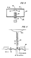
- Fig. 4 show the optical system of Fig. 1 modified by the replacement of the two-row array with an array 40 having a single row 42 of gradient index fibers. The array is biased by a combination of biased spring 43a and spring roller 43 to ride against the surface of a sinusoidal linear rack 44 attached to platen 12.
- array 40 is oscillated laterally.
- the exposure zone 18 is typically about 5 mm.
- rack 44 should be configured so as to enable lens array 40 to make at least one translational excursion TE, during the time it takes belt 16 to travel 5 mm.
- Other mechanisms may be used to achieve sinusoidal movement such as enclosing rack 44 and roller 43 within an enclosed channel. From Figure 3 it will be seen that the one-row array is characterized by having a useful a/b parameter of between 1.25 and 7.
- Equation (3) shows that the efficiency is maximized when the a/b parameter is 1.5.
- Figure 8 shows a plot 48 of exposure modulation vs. a/b parameter for a two-row gradient index lens array used in a printer or RIS. Plot 48 has maximum and minimum value 48 t-z and 48 a-g respectively.
- a large (10%) and unacceptable value of exposure modulation results.
- efficiency is reduced from optimum by about 25%. For scanner or printer applications, a reduction of 30% in efficiency will result in a 30% reduction in total exposure.
- Fig. 9 shows a RIS optical system 50 embodying the principles of the present invention.
- Lamp assembly 52 is disposed on each side of scanning slit 54 to provide a narrow incremental band of illumination along the scan strip.
- Two-row gradient index lens array 56 is disposed intermediate the moving document platen 58 and a linear photosensor array 60 and in a position to form a unity magnification image of the scanned portion of the document onto the surface of array 60.
- successive line scans are made across a document 62 by array 60 as the platen is moved past scanning slit 54.
- the exposure zone for this case, is defined by the edge of the photosensor array pixels.
- the individual viewing elements that comprise array 60 are sampled successively as each line is scanned to produce a stream of image signals or pixels for each line scanned.
- the individual pixels produced each comprises a discrete voltage representative of the image area of document 62 viewed by the individual lenslets comprising array 60.
- One commonly available full-width scanning array is a FIE-8A linear array manufactured by Fuji Xerox Co., Ltd..
- the exposure modulation for the two-row scanner array has a period which is related to the size and spacing of the individual fibers comprising the two rows and is further defined by whether the a/b selection is at a modulation maximum, minimum or intermediate.
- Fig. 10 shows the three possibilities and their relation to the gradient index fibers of lens array 58. The maximum corresponds to peaks 48 t-z while the minimum coverage to valleys 48a-g. Again, a small lateral motion (left to right) of the array will reduce the modulation but there are optimum motions during a given exposure period. The optimum motion at maximum modulation is bR/2 and bR/4 for minimum modulation.
- Typical values for R are .5325 mm and 0.5485 mm for bR/2.
- the excursion time is considerably reduced because the exposure zone (at array 60) is typically 0.08 mm for a 120 spots per cm application, a much smaller exposure zone value than for the 5 mm copier case.
- lens 56 should make at least one transitional excursion TE during the time it takes the platen to travel 0.08 mm.
- array 56 rides in a spring biased relation with sinusoidal linear rack 64, mounted along platen 62.
- a linear light bar such as an LED array defines the light entering the array, and therefore also defines the exposure zone at a photoreceptor surface.
- Other image light bar examples are liquid crystal shutters (LCS).
- the exposure zone for printing applications is approximately the same 0.08 mm width for a 120 spots per cm application.
- a pizeoelectric transducer may be attached to the lens array and periodically addressed to produce the required motion as is known in the art.
- the main feature of the invention is the oscillation of the lens in a cross-scan, or array direction (lateral to the scan direction). This motion moves the exposure profile to fill in non-uniform areas, reducing exposure modulation and improving uniformity. This motion is not accompanied by any blurring of the image. If the invention is practiced in a copier mode, a one-row array is enabled, permitting savings in lens array procurement and assembly costs. If the usage is in a scanner or printer environment, the invention permits the two-row lens array to be operated at higher efficiency levels.
- the prescribed oscillation of the lens array will yield some improvement of the exposure modulation.
- the prescribed oscillation would work for a one-row array and reduce cost, if sufficient light (printer) or sensitivity (scanner) were available.
Applications Claiming Priority (2)
| Application Number | Priority Date | Filing Date | Title |
|---|---|---|---|
| US06/890,204 US4982222A (en) | 1986-07-28 | 1986-07-28 | Imaging system utilizing an oscillating gradient index lens array |
| US890204 | 1986-07-28 |
Publications (3)
| Publication Number | Publication Date |
|---|---|
| EP0257798A2 true EP0257798A2 (de) | 1988-03-02 |
| EP0257798A3 EP0257798A3 (en) | 1989-07-26 |
| EP0257798B1 EP0257798B1 (de) | 1993-12-22 |
Family
ID=25396384
Family Applications (1)
| Application Number | Title | Priority Date | Filing Date |
|---|---|---|---|
| EP87306524A Expired - Lifetime EP0257798B1 (de) | 1986-07-28 | 1987-07-23 | Abbildungssystem mit einer oszillierenden Anordnung von Gradientenlinsen |
Country Status (5)
| Country | Link |
|---|---|
| US (1) | US4982222A (de) |
| EP (1) | EP0257798B1 (de) |
| JP (1) | JPS6336653A (de) |
| CA (1) | CA1285604C (de) |
| DE (1) | DE3788545T2 (de) |
Cited By (4)
| Publication number | Priority date | Publication date | Assignee | Title |
|---|---|---|---|---|
| WO1991007675A1 (en) * | 1989-11-14 | 1991-05-30 | Hicks John W | Flying spot endoscope |
| US5103497A (en) * | 1989-11-14 | 1992-04-07 | Hicks John W | Flying spot endoscope |
| EP0596664A1 (de) * | 1992-11-04 | 1994-05-11 | Canon Kabushiki Kaisha | Linsenanordnung und Engkontakt-Bildsensor mit solcher |
| EP0878310A1 (de) * | 1997-05-13 | 1998-11-18 | Canon Kabushiki Kaisha | Bilderzeugungsgerät |
Families Citing this family (10)
| Publication number | Priority date | Publication date | Assignee | Title |
|---|---|---|---|---|
| US5233469A (en) * | 1987-10-22 | 1993-08-03 | Canon Kabushiki Kaisha | Imaging optical system using index distribution type optical elements |
| US5150151A (en) * | 1989-03-09 | 1992-09-22 | Canon Kabushiki Kaisha | Reflecting device and pattern transfer apparatus using the same |
| US5436691A (en) * | 1994-05-05 | 1995-07-25 | Xerox Corporation | Copier with anamorphic magnification imaging system |
| US6469728B1 (en) | 1995-12-18 | 2002-10-22 | Xerox Corporation | LED printbars with depth of focus enhancement |
| US5801849A (en) * | 1996-10-21 | 1998-09-01 | Telesensory Corporation | Image reading device and document scanning system |
| US6088166A (en) * | 1998-12-22 | 2000-07-11 | Dicon Fiberoptics, Inc. | Miniaturization of gradient index lens used in optical components |
| US6975949B2 (en) * | 2004-04-27 | 2005-12-13 | Xerox Corporation | Full width array scanning spectrophotometer |
| TWI456777B (zh) * | 2011-07-28 | 2014-10-11 | Univ Nat Taiwan Science Tech | 多透鏡陣列之集光模組 |
| EP3575845B1 (de) | 2018-05-30 | 2021-07-14 | Depixus | Mehrkanalige nahbildgebungsvorrichtung |
| EP3686642A1 (de) | 2019-01-24 | 2020-07-29 | Depixus | Mehrkanalige nahbildgebungsvorrichtung |
Citations (6)
| Publication number | Priority date | Publication date | Assignee | Title |
|---|---|---|---|---|
| US3977777A (en) * | 1973-11-07 | 1976-08-31 | Minolta Camera Kabushiki Kaisha | Image transmission device for slit scanning type photocopying machine |
| DE2757386B2 (de) * | 1977-12-22 | 1981-02-26 | Agfa-Gevaert Ag, 5090 Leverkusen | Belichtungsanordnung für Kopiergeräte |
| US4314282A (en) * | 1980-04-14 | 1982-02-02 | Xerox Corporation | Multifunction graphic engine based on an oscillating scanner |
| DE3432392A1 (de) * | 1983-09-05 | 1985-04-04 | Olympus Optical Co., Ltd., Tokio/Tokyo | Bildaufnahme- und beobachtungsvorrichtung fuer ein endoskop |
| US4509826A (en) * | 1983-04-11 | 1985-04-09 | Xerox Corporation | Optical image staggering/destaggering arrangement for multiple array scanning system |
| EP0178195A1 (de) * | 1984-08-14 | 1986-04-16 | Thomson-Csf | Bildübertragung mittels eines optischen Kabels |
Family Cites Families (6)
| Publication number | Priority date | Publication date | Assignee | Title |
|---|---|---|---|---|
| US3217594A (en) * | 1963-02-27 | 1965-11-16 | Simmon Brothers Inc | Photographic printer and enlarger and light mixing device therefor |
| US3194142A (en) * | 1963-09-26 | 1965-07-13 | Mosaic Fabrications Inc | Optical image transfer device |
| DE1278136B (de) * | 1966-03-17 | 1968-09-19 | Schneider Co Optische Werke | Verfahren und Vorrichtung zur Bilduebertragung mittels faseroptischer Bauelemente |
| JPS53304B2 (de) * | 1973-08-07 | 1978-01-07 | ||
| US4098550A (en) * | 1976-03-29 | 1978-07-04 | Randolph John W | Omni-directional moving picture taking and exhibiting apparatus |
| US4349248A (en) * | 1980-04-23 | 1982-09-14 | Xerox Corporation | Gradient index lens array with improved exposure uniformity |
-
1986
- 1986-07-28 US US06/890,204 patent/US4982222A/en not_active Expired - Fee Related
-
1987
- 1987-06-25 CA CA000540584A patent/CA1285604C/en not_active Expired - Fee Related
- 1987-07-21 JP JP62182119A patent/JPS6336653A/ja active Pending
- 1987-07-23 DE DE3788545T patent/DE3788545T2/de not_active Expired - Fee Related
- 1987-07-23 EP EP87306524A patent/EP0257798B1/de not_active Expired - Lifetime
Patent Citations (6)
| Publication number | Priority date | Publication date | Assignee | Title |
|---|---|---|---|---|
| US3977777A (en) * | 1973-11-07 | 1976-08-31 | Minolta Camera Kabushiki Kaisha | Image transmission device for slit scanning type photocopying machine |
| DE2757386B2 (de) * | 1977-12-22 | 1981-02-26 | Agfa-Gevaert Ag, 5090 Leverkusen | Belichtungsanordnung für Kopiergeräte |
| US4314282A (en) * | 1980-04-14 | 1982-02-02 | Xerox Corporation | Multifunction graphic engine based on an oscillating scanner |
| US4509826A (en) * | 1983-04-11 | 1985-04-09 | Xerox Corporation | Optical image staggering/destaggering arrangement for multiple array scanning system |
| DE3432392A1 (de) * | 1983-09-05 | 1985-04-04 | Olympus Optical Co., Ltd., Tokio/Tokyo | Bildaufnahme- und beobachtungsvorrichtung fuer ein endoskop |
| EP0178195A1 (de) * | 1984-08-14 | 1986-04-16 | Thomson-Csf | Bildübertragung mittels eines optischen Kabels |
Cited By (7)
| Publication number | Priority date | Publication date | Assignee | Title |
|---|---|---|---|---|
| WO1991007675A1 (en) * | 1989-11-14 | 1991-05-30 | Hicks John W | Flying spot endoscope |
| US5103497A (en) * | 1989-11-14 | 1992-04-07 | Hicks John W | Flying spot endoscope |
| AU637234B2 (en) * | 1989-11-14 | 1993-05-20 | John Wilbur Hicks | Flying spot endoscope |
| EP0596664A1 (de) * | 1992-11-04 | 1994-05-11 | Canon Kabushiki Kaisha | Linsenanordnung und Engkontakt-Bildsensor mit solcher |
| US5661540A (en) * | 1992-11-04 | 1997-08-26 | Canon Kabushiki Kaisha | Lens array and close contact type image sensor using the same |
| EP0878310A1 (de) * | 1997-05-13 | 1998-11-18 | Canon Kabushiki Kaisha | Bilderzeugungsgerät |
| US6088164A (en) * | 1997-05-13 | 2000-07-11 | Canon Kabushiki Kaisha | Image forming apparatus having a lens array |
Also Published As
| Publication number | Publication date |
|---|---|
| US4982222A (en) | 1991-01-01 |
| JPS6336653A (ja) | 1988-02-17 |
| DE3788545T2 (de) | 1994-05-26 |
| EP0257798A3 (en) | 1989-07-26 |
| EP0257798B1 (de) | 1993-12-22 |
| DE3788545D1 (de) | 1994-02-03 |
| CA1285604C (en) | 1991-07-02 |
Similar Documents
| Publication | Publication Date | Title |
|---|---|---|
| EP0257798B1 (de) | Abbildungssystem mit einer oszillierenden Anordnung von Gradientenlinsen | |
| US5450157A (en) | Imaging system using a gradient index lens array with improved depth of focus | |
| US4467195A (en) | Information detecting apparatus | |
| KR100237500B1 (ko) | 영상주사용 광학적 주사요소 및 광학적 주사요소 제조방법 | |
| US4509826A (en) | Optical image staggering/destaggering arrangement for multiple array scanning system | |
| EP3550816B1 (de) | Lesemodul, bildlesevorrichtung damit und bilderzeugungsvorrichtung | |
| EP0448275B1 (de) | Optisches Dokumentabtastsystem | |
| US4349248A (en) | Gradient index lens array with improved exposure uniformity | |
| US5166999A (en) | High resolution print bar system | |
| US6175429B1 (en) | Document reader and method for adjusting its focus | |
| US4373780A (en) | Image transmitting system utilizing a gradient index lens | |
| EP0143357B1 (de) | Dokumentenabtaster und optische Vorrichtung dafür | |
| US4259696A (en) | Apparatus and method for jet drop copying with an array of jets and photodetectors | |
| JP2007045094A (ja) | 走査光学系及びそれを用いた画像形成装置 | |
| US5216738A (en) | Fiber optic bundle and method of manufacture | |
| JPS62262567A (ja) | 情報読取装置 | |
| US4678311A (en) | Multi-magnification short focal length imaging system | |
| US4258395A (en) | Document scanning system | |
| JPS6224984B2 (de) | ||
| EP0038693B1 (de) | Optisches Abbildungssystem | |
| US4291973A (en) | Scanning system | |
| EP0782928B1 (de) | Farbxerographischer Drucker mit vielfachen linearen Reihen von oberflächenemittierenden Lasern mit gleichen Wellenlängen | |
| JPS61212960A (ja) | 画像読取装置 | |
| JPH04153049A (ja) | 結像素子及び画像読取装置及び光書込ヘッド | |
| JPH07301865A (ja) | 複写機 |
Legal Events
| Date | Code | Title | Description |
|---|---|---|---|
| PUAI | Public reference made under article 153(3) epc to a published international application that has entered the european phase |
Free format text: ORIGINAL CODE: 0009012 |
|
| AK | Designated contracting states |
Kind code of ref document: A2 Designated state(s): DE FR GB IT |
|
| PUAL | Search report despatched |
Free format text: ORIGINAL CODE: 0009013 |
|
| RHK1 | Main classification (correction) |
Ipc: G02B 3/00 |
|
| AK | Designated contracting states |
Kind code of ref document: A3 Designated state(s): DE FR GB IT |
|
| 17P | Request for examination filed |
Effective date: 19900118 |
|
| 17Q | First examination report despatched |
Effective date: 19920213 |
|
| GRAA | (expected) grant |
Free format text: ORIGINAL CODE: 0009210 |
|
| AK | Designated contracting states |
Kind code of ref document: B1 Designated state(s): DE FR GB IT |
|
| REF | Corresponds to: |
Ref document number: 3788545 Country of ref document: DE Date of ref document: 19940203 |
|
| ET | Fr: translation filed | ||
| ITF | It: translation for a ep patent filed |
Owner name: MODIANO & ASSOCIATI S.R.L. |
|
| PLBE | No opposition filed within time limit |
Free format text: ORIGINAL CODE: 0009261 |
|
| STAA | Information on the status of an ep patent application or granted ep patent |
Free format text: STATUS: NO OPPOSITION FILED WITHIN TIME LIMIT |
|
| 26N | No opposition filed | ||
| PGFP | Annual fee paid to national office [announced via postgrant information from national office to epo] |
Ref country code: FR Payment date: 20010712 Year of fee payment: 15 |
|
| PGFP | Annual fee paid to national office [announced via postgrant information from national office to epo] |
Ref country code: DE Payment date: 20010716 Year of fee payment: 15 |
|
| PGFP | Annual fee paid to national office [announced via postgrant information from national office to epo] |
Ref country code: GB Payment date: 20010718 Year of fee payment: 15 |
|
| REG | Reference to a national code |
Ref country code: GB Ref legal event code: IF02 |
|
| PG25 | Lapsed in a contracting state [announced via postgrant information from national office to epo] |
Ref country code: GB Free format text: LAPSE BECAUSE OF NON-PAYMENT OF DUE FEES Effective date: 20020723 |
|
| PG25 | Lapsed in a contracting state [announced via postgrant information from national office to epo] |
Ref country code: DE Free format text: LAPSE BECAUSE OF NON-PAYMENT OF DUE FEES Effective date: 20030201 |
|
| GBPC | Gb: european patent ceased through non-payment of renewal fee |
Effective date: 20020723 |
|
| PG25 | Lapsed in a contracting state [announced via postgrant information from national office to epo] |
Ref country code: FR Free format text: LAPSE BECAUSE OF NON-PAYMENT OF DUE FEES Effective date: 20030331 |
|
| REG | Reference to a national code |
Ref country code: FR Ref legal event code: ST |
|
| PG25 | Lapsed in a contracting state [announced via postgrant information from national office to epo] |
Ref country code: IT Free format text: LAPSE BECAUSE OF NON-PAYMENT OF DUE FEES Effective date: 20050723 |