EP0256580A1 - Gyratorschaltung, die eine Induktanz simuliert - Google Patents
Gyratorschaltung, die eine Induktanz simuliert Download PDFInfo
- Publication number
- EP0256580A1 EP0256580A1 EP87201397A EP87201397A EP0256580A1 EP 0256580 A1 EP0256580 A1 EP 0256580A1 EP 87201397 A EP87201397 A EP 87201397A EP 87201397 A EP87201397 A EP 87201397A EP 0256580 A1 EP0256580 A1 EP 0256580A1
- Authority
- EP
- European Patent Office
- Prior art keywords
- terminal
- circuit
- transistor
- gyrator
- stage
- Prior art date
- Legal status (The legal status is an assumption and is not a legal conclusion. Google has not performed a legal analysis and makes no representation as to the accuracy of the status listed.)
- Withdrawn
Links
Images


Classifications
-
- H—ELECTRICITY
- H03—ELECTRONIC CIRCUITRY
- H03H—IMPEDANCE NETWORKS, e.g. RESONANT CIRCUITS; RESONATORS
- H03H11/00—Networks using active elements
- H03H11/46—One-port networks
- H03H11/48—One-port networks simulating reactances
- H03H11/50—One-port networks simulating reactances using gyrators
-
- H—ELECTRICITY
- H03—ELECTRONIC CIRCUITRY
- H03H—IMPEDANCE NETWORKS, e.g. RESONANT CIRCUITS; RESONATORS
- H03H11/00—Networks using active elements
- H03H11/02—Multiple-port networks
- H03H11/04—Frequency selective two-port networks
- H03H11/08—Frequency selective two-port networks using gyrators
-
- H—ELECTRICITY
- H03—ELECTRONIC CIRCUITRY
- H03H—IMPEDANCE NETWORKS, e.g. RESONANT CIRCUITS; RESONATORS
- H03H11/00—Networks using active elements
- H03H11/02—Multiple-port networks
- H03H11/40—Impedance converters
- H03H11/42—Gyrators
Definitions
- the invention relates to a gyrator circuit formed on the one hand by a first and a second transconductive amplifiers, respectively A and B, of opposite transconductances, connected in parallel between a first terminal a and a second terminal b, and formed by on the other hand, a first capacitance C 1 mounted between said first terminal a and a third terminal m, this gyrator circuit simulating an inductance Lg mounted between said second terminal b and said third terminal m, and comprising means for controlling its factor quality Q.
- the invention also relates to a resonant circuit including this inductance Lg.
- the invention finds its application in the production of microwave filters, as well as in the production of oscillators.
- a gyrator circuit simulating an inductance and included in a resonant circuit with a filter function is known from the publication in "IEEE, J. Solid-State Circuits, Vol. SC-15, pp 963-968, Dec. 1980", from l article entitled “Gyrator Video Filter IC with Automatic Tuning” by Kenneth W. MOLDING et alii.
- This document describes a gyrator circuit formed by two differential amplifiers, current sources, voltage-controlled, of opposite transconductances, mounted head to tail in parallel, and charged on two capacities.
- the technology used to make this circuit includes bipolar transistors whose threshold voltage is such that it induces in the amplifiers a significant phase shift which results in a negative resistance greater in absolute value than the positive resistance due to losses, risking d '' cause the circuit to oscillate.
- This circuit is, for this reason, provided with an additional resistance intended to be added to the resistance positive due to losses, in order to compensate for this defect and avoid oscillation.
- the quality factor of such a circuit being inversely proportional to the result of the resistance due to the phase shift and of the resistance due to the losses, this additional resistance must therefore be low.
- this additional resistor is placed in series with one of the load capacities of the gyrator and is connected to a bias voltage intended to allow the tuning of the tuning of the resonator.
- an auxiliary gyrator circuit tuned on a quartz oscillator, is used to tune the gyrator-filter by supplying the bias voltage of the capacitors. This system then allows closed loop control of the auxiliary gyrator circuit, but is based on the fact that the gyrator-filter must follow.
- this object is achieved by means of a circuit as described in the preamble, characterized in that the first transconductive amplifier circuit A is formed by two inverting amplifier stages P, and F 2 connected in series, in that the second transconductive amplifier circuit B is formed by an inverting amplifier stage P 3 , and in that the means for controlling the quality factor Q is formed by a first means Ps for acting on the output conductance g 2 of the gyrator, and a second means P, for acting on the phase shift m between the output current and the control voltage of the gyrator.
- the proposed gyrator circuit is used to simulate an inductance in order to produce a resonant circuit formed by this inductance denoted later L 2 and with a capacitor C 2 .
- the output impedance is an inductance L 2 defined by:
- a gyrator is, in a known state of the art, formed of two transconductive amplifiers, that is to say sources of current, voltage-controlled, of opposite transconductances, mounted head to tail in parallel.
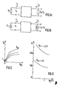
- This gyrator therefore comprises, as shown in FIG. 3a, an amplifier A and an inverting amplifier B.
- the gyration conductance g o is then linked to the conductances of each of the amplifiers, gmA and gmB respectively, by the relation:
- the capacitor C 1 connected to the input E of the gyrator circuit is then transformed into the inductance L 2
- the capacitance C 1 is lossless, the gyrator without losses, the admittance of gyration is real, and the inductance L 2 generated is then pure.
- the matrix is of the form: with for the currents i 1 and i 2 at the input and at the output as a function of the voltages v 1 and v 2 at the input and at the output as shown in FIG. 1a.
- the susceptible parts of the admittances y11 and y 22 of input and output of the gyrator, respectively jb 11 and jb 22 , are added to the susceptance of the load capacity Ci and to the output inductance L 2 , so that the latter are modified, in particular L 2 takes the value Lg.
- the total conductance is expressed by: relation in which g C is the conductance of the capacitor C 1 .
- g L is the conductance of the circuit at the terminals of which the inductance L 2 is mounted.
- the quality factor is controlled and the precision on the value of the inductance generated from a capacitance is obtained by controlling the phase shift ⁇ on the one hand and the inductance g 2 on the other go.
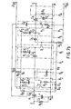
- FIG. 3b gives an equivalent block diagram of the circuit of FIG. 2.
- Part P 2 is an inverter stage, as well as parts P 1 and P 3 .
- Part P 4 is a buffer stage (in English BUFFER).
- the inverters P 1 and P 2 are in series with the stage buffer P 4 and are equivalent to a non-inverting amplifier such as A ( Figure 3a).
- the part P 3 is equivalent to the inverting amplifier B of FIG. 3a.
- these amplifiers are therefore of opposite polarity and mounted head to tail in parallel between nodes a and b.
- the capacitor C 1 placed at the input E, between the node a and the mass m is transformed by the gyrator into an inductance Lg placed between the node b and the mass m.
- the capacitor C 2 placed in parallel on Lg forms the resonant circuit LC sought.
- the signal to be filtered at frequency F, or any other signal for any other application, is applied to the gyrator device according to the invention at the input INP of an amplifier P A (see FIG. 3b).
- the filtered signal is collected on the output S (see figures 2, 3b, 3c).
- Each inverter stage Pt, P 2 , P 3 consists of an inverter transistor Tt, T 2 , T 3 and an active load T'i, T ' 2 , T' 3, respectively .
- Each stage is continuously isolated from the preceding and the following, by a capacitor, such as C 3 , C 4 , C 5 , C G , just as the input INP is by a capacitor C7.
- the transistors used to make the circuit according to the invention are preferably field effect transistors of the MESFET type which have advantageous properties in the production of circuits operating at high frequencies.
- the amplifier stages produced by means of these transistors usually show a very small gain, this gain being however improved in a known manner by the use of an active load.
- an active load has the advantage of providing a high dynamic load, which promotes the gain, the latter being proportional to the load, and of providing a lower continuous load, which does not not deteriorate the gain by too large a direct current.
- the use of the active load supposes a very delicate polarization of the two transistors connected in series, the inverter transistor and the load transistor, these two transistors each behaving like two current sources connected in series. In fact, in such an arrangement, the slightest difference in polarization can cause one or the other of these transistors to be desaturated.
- each inverting amplifier stage of the circuit the active load constituted by each of the transistors T 'is polarized as shown in FIG. 4a.
- the load transistor T ' is mounted as a common drain on the positive DC power supply V DD , its source is connected to the common drain point of the inverter transistor T and of output 0 of the inverter stage.
- the inverter transistor T is mounted so that its source is connected to ground, and its gate, on which the input I of the stage is applied, is polarized by a resistor R placed between 1 and a negative potential -V GG .
- the gate of the charge transistor T ' is polarized on the one hand by means of a resistor R' connected to a positive supply VA and on the other hand by means of a capacitor C 'connected to the point o.
- the voltage VA is taken from the common point between the resistor Rp and the level shift diode Dp, the resistor Rp being on the other hand connected to the voltage V DD and the diode Dp connected to ground.
- a voltage -V B defined by -V GG ⁇ -V B ⁇ 0 is calibrated by the same method as V A , that is to say with respect to the mass by a diode D S and with respect to -V GG by a resistor Rs (see FIG. 2).
- the reversing stage provided with such a load behaves as according to the circuit shown in FIG. 4b, that is to say as with a conventional active load.
- the inverter stage behaves as according to the circuit shown in FIG. 4c.
- the transistor T 'then behaves as a follower, that is to say that its source voltage follows the voltage V A. It is then, no longer a current source as before, but a voltage source, with a low output impedance.
- the inverter stage is then formed no longer of two current sources in series as it was known, but of a current source (T) in series with a voltage source (T '). The operation of each inverter stage is thus optimized.
- the stage Pi only includes as elements corresponding to the assembly described above that the elements T ' 1 , R' 1 , C ' 1 .
- the device according to the invention which makes it possible to control the phase shift introduced by the gyrator, comprises two parts denoted Ps and Ps, delimited in FIG. 2 by dotted lines. The part Ps is precisely applied to the gate of the transistor T 1 in the expected position for a resistor R 1 in accordance with the diagram in FIG. 4a.
- the part Ps of the phase shift control of the gyrator according to the invention consists of a transistor T d whose drain is connected to the gate of the transistor T 1 , whose source is connected to the voltage -V B and whose gate is brought to a control voltage V d (see FIG. 2).
- This voltage V d is provided such that the transistor T d works in an area where its drain current I D is close to zero (but equal to 0 continuously), for example in the delimited area Z by dotted lines in FIG. 5 which represents the characteristics I D as a function of the drain-source voltage V DS for different gate-source voltages V GS .
- the transistor T D operates in a region where the characteristics are linear and behaves like a variable resistor R d whose value is electrically controlled by the voltage Vd (see FIG. 3b).
- this resistor R d is located in parallel on the output S and makes it possible to act on the output conductance g 2 of the gyrator.
- the part P 6 also makes it possible to act on the phase shift 9 of the gyrator.
- the part P 4 of the gyrator consists of a buffer stage (in English BUFFER) formed by a transistor mounted as a drain common to V DD T 4 , and by a current source transistor T ' 4, the source and the grid of which are short-circuited are connected to ground.
- the part P 6 consists of a diode D ⁇ in series with a capacitor C ' ⁇ , this arrangement being placed between the common point of the transistors T 4 and T' 4 of the buffer stage and the ground.
- the set P 6 thus forms a C ⁇ variable capacitance whose value is a function of the ⁇ V control voltage applied to the common point between the diode D and the capacitor C ⁇ ' ⁇ .
- the term g 2 is controlled by the variable resistance R d . This resistance varies by producing an increase in the term g 2 which causes a decrease in the quality factor Q.
- variable capacitance C ⁇ acts by increasing the absolute value of the phase shift ⁇ therefore by increasing the quality factor Q.
- the amplifier P A on the INP input of which is applied the signal F to be filtered itself consists of an inverting amplifier stage.
- This stage comprises (see FIG. 2) a transistor T A , the charge of which is common to transistor T 3 , and which is biased with respect to the negative voltage -V GG via the resistor R A.
- This system makes it possible to produce the circuit by means of field effect transistors of the MESFET type, which is particularly advantageous for operation at high frequencies.
- the circuit according to the invention is made up of elements whose values are given in table I, where W is the gate width of the transistors, with: pinch tension
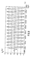
- FIG. 6 shows the values obtained for the quality factor Q as a function of the values of the control voltages V ⁇ and V d of the two adjustment elements of the gyrator according to the invention. On average, this quality factor is between 100 and 250.
- this monolithically integrated circuit on a group III-V material such as gallium arsenide for example. If it is produced by means of the elements whose characteristics are given in table I, it then occupies an area of approximately 0.25 mm 2, and can operate in a frequency range between 40 MHz and 2 kHz.
- this circuit can for other applications, and by providing suitable elements, be used on the contrary as an oscillator.
- the part P 6 of the circuit makes it possible to achieve the negative resistance necessary for the oscillation.
- the adjustment of the oscillation frequency is obtained by the simultaneous variation of the input and output capacities C 1 and C 2 which will advantageously be varicaps.
- the oscillation frequency is deduced from the relation: If L 2 was fixed, as is the case in an oscillator conventionally known to those skilled in the art, the oscillation frequency can be expressed by: where K 'is a constant. On the contrary according to the invention, since L 2 is adjustable, the oscillation frequency is expressed by: which represents a great advantage compared to the state of the art of the fact that one will easily obtain high oscillation frequencies with very small capacities. When you know that in the field of circuit integration, the area occupied by the capacitors poses a big problem, so that certain high-value capacitors cannot even be integrated, the advantage provided by the circuit according to the invention when used as an oscillator appears immediately.
- the oscillator according to the invention has still other advantages.
- the gyrator circuit used as an oscillator in which the transistors are field effect transistors of the MESFET type and of which all the components are very small. Besides the advantage of high frequencies, the circuit is very compact and consumes very little. The characteristics of this circuit are gathered in table II and the diagram of the oscillator circuit is represented on figure 7a.
- the control voltage V C makes it possible to change the value of the capacitors C 1 and C 2 , which are constituted by diodes D 1 and D 2 , and therefore the frequency. It will be noted that resistors R E and R S have been added in parallel on C 1 and C 2 and that insulation capacities CE and C S have also been added.
- Stage P5 can also be deleted.
- the circuit consumption is then 100 mW.
- the frequency band is from 2 GHz to 5 GHz.
- Figure 8 shows the oscillations obtained on the output signal V S (in V) as a function of time t, at 3 GHz.
- the stage P 4 is eliminated, all the transistors pass to 10 ⁇ m and the consumption to 40 mW. But the frequency band is slightly narrower and centered on 2.8 GHz-3.5 GHz.
Applications Claiming Priority (2)
| Application Number | Priority Date | Filing Date | Title |
|---|---|---|---|
| FR8611032A FR2602380B1 (fr) | 1986-07-30 | 1986-07-30 | Circuit gyrateur simulant une inductance |
| FR8611032 | 1986-07-30 |
Publications (1)
| Publication Number | Publication Date |
|---|---|
| EP0256580A1 true EP0256580A1 (de) | 1988-02-24 |
Family
ID=9337877
Family Applications (1)
| Application Number | Title | Priority Date | Filing Date |
|---|---|---|---|
| EP87201397A Withdrawn EP0256580A1 (de) | 1986-07-30 | 1987-07-21 | Gyratorschaltung, die eine Induktanz simuliert |
Country Status (5)
| Country | Link |
|---|---|
| US (1) | US4812785A (de) |
| EP (1) | EP0256580A1 (de) |
| JP (1) | JPS6338317A (de) |
| KR (1) | KR880002322A (de) |
| FR (1) | FR2602380B1 (de) |
Cited By (3)
| Publication number | Priority date | Publication date | Assignee | Title |
|---|---|---|---|---|
| EP0365091A2 (de) * | 1988-10-21 | 1990-04-25 | Philips Electronics Uk Limited | Filterschaltungsanordnung |
| FR2763681A1 (fr) * | 1997-05-26 | 1998-11-27 | Canon Kk | Dispositif de determination d'une quantite de produit consommable presente dans un reservoir et dispositif d'impression de documents correspondant |
| DE102014008990A1 (de) | 2014-06-13 | 2015-12-17 | Dietmar Dreyer | Halbleiterverstärker zur Speicherung von elektrischer Energie auf der Basis eines generierten Schwingkreises |
Families Citing this family (42)
| Publication number | Priority date | Publication date | Assignee | Title |
|---|---|---|---|---|
| GB2208340B (en) * | 1987-07-17 | 1992-01-22 | Plessey Co Plc | Electrical circuits |
| JP2784467B2 (ja) * | 1987-12-04 | 1998-08-06 | 日本電信電話株式会社 | 電圧制御発振器 |
| EP0398728B1 (de) * | 1989-05-19 | 1994-07-13 | Murata Manufacturing Co., Ltd. | Keramisches resonanzartiges Elektrostatikfühlergerät |
| JPH04284005A (ja) * | 1991-03-13 | 1992-10-08 | Sharp Corp | 発振回路 |
| US5287036A (en) * | 1992-03-02 | 1994-02-15 | Motorola, Inc. | Method and apparatus for acoustic wave inductance |
| JPH05283972A (ja) * | 1992-04-03 | 1993-10-29 | Nec Corp | フィルタ回路 |
| US5347238A (en) * | 1993-07-06 | 1994-09-13 | Trw Inc. | Bipolar microwave monolithic voltage controlled oscillator using active inductors |
| KR19990035935A (ko) * | 1996-05-28 | 1999-05-25 | 엠. 제이. 엠. 반캄 | 전기 통신 장치용 부속 장치 |
| US5850163A (en) * | 1997-03-31 | 1998-12-15 | Sun Microsystems, Inc. | Active inductor oscillator with wide frequency range |
| KR19990057175A (ko) * | 1997-12-29 | 1999-07-15 | 김영환 | 자이레이터를 이용한 임피던스 정합장치 |
| US6104230A (en) * | 1998-09-16 | 2000-08-15 | Conexant Systems, Inc. | Electronic inductor circuit using cascoded transistors |
| US6184747B1 (en) | 1999-05-13 | 2001-02-06 | Honeywell International Inc. | Differential filter with gyrator |
| US6236238B1 (en) | 1999-05-13 | 2001-05-22 | Honeywell International Inc. | Output buffer with independently controllable current mirror legs |
| US7015789B1 (en) * | 1999-05-13 | 2006-03-21 | Honeywell International Inc. | State validation using bi-directional wireless link |
| US6727816B1 (en) | 1999-05-13 | 2004-04-27 | Honeywell International Inc. | Wireless system with variable learned-in transmit power |
| US6901066B1 (en) | 1999-05-13 | 2005-05-31 | Honeywell International Inc. | Wireless control network with scheduled time slots |
| US6429733B1 (en) | 1999-05-13 | 2002-08-06 | Honeywell International Inc. | Filter with controlled offsets for active filter selectivity and DC offset control |
| DE19958096B4 (de) * | 1999-12-02 | 2012-04-19 | Telefonaktiebolaget Lm Ericsson (Publ) | Verfahren zum Entwerfen einer Filterschaltung |
| US6583661B1 (en) | 2000-11-03 | 2003-06-24 | Honeywell Inc. | Compensation mechanism for compensating bias levels of an operation circuit in response to supply voltage changes |
| US7826373B2 (en) * | 2005-01-28 | 2010-11-02 | Honeywell International Inc. | Wireless routing systems and methods |
| US8085672B2 (en) * | 2005-01-28 | 2011-12-27 | Honeywell International Inc. | Wireless routing implementation |
| US7742394B2 (en) * | 2005-06-03 | 2010-06-22 | Honeywell International Inc. | Redundantly connected wireless sensor networking methods |
| US7848223B2 (en) * | 2005-06-03 | 2010-12-07 | Honeywell International Inc. | Redundantly connected wireless sensor networking methods |
| US8463319B2 (en) * | 2005-06-17 | 2013-06-11 | Honeywell International Inc. | Wireless application installation, configuration and management tool |
| US7394782B2 (en) * | 2005-07-14 | 2008-07-01 | Honeywell International Inc. | Reduced power time synchronization in wireless communication |
| US7801094B2 (en) * | 2005-08-08 | 2010-09-21 | Honeywell International Inc. | Integrated infrastructure supporting multiple wireless devices |
| US20070030816A1 (en) * | 2005-08-08 | 2007-02-08 | Honeywell International Inc. | Data compression and abnormal situation detection in a wireless sensor network |
| US7289466B2 (en) * | 2005-10-05 | 2007-10-30 | Honeywell International Inc. | Localization for low cost sensor network |
| US7603129B2 (en) * | 2005-10-05 | 2009-10-13 | Honeywell International Inc. | Localization identification system for wireless devices |
| US8811231B2 (en) * | 2005-10-21 | 2014-08-19 | Honeywell International Inc. | Wireless transmitter initiated communication systems |
| US8644192B2 (en) * | 2005-10-21 | 2014-02-04 | Honeywell International Inc. | Wireless transmitter initiated communication methods |
| US20070097873A1 (en) * | 2005-10-31 | 2007-05-03 | Honeywell International Inc. | Multiple model estimation in mobile ad-hoc networks |
| US8285326B2 (en) * | 2005-12-30 | 2012-10-09 | Honeywell International Inc. | Multiprotocol wireless communication backbone |
| US8413227B2 (en) * | 2007-09-28 | 2013-04-02 | Honeywell International Inc. | Apparatus and method supporting wireless access to multiple security layers in an industrial control and automation system or other system |
| US7986701B2 (en) * | 2008-06-13 | 2011-07-26 | Honeywell International Inc. | Wireless building control system bridge |
| US8884198B2 (en) * | 2010-01-22 | 2014-11-11 | Continental Automotive Systems, Inc. | Parametric temperature regulation of induction heated load |
| US8365703B2 (en) * | 2010-01-22 | 2013-02-05 | Continental Automotive Systems Us, Inc. | Switch-mode synthetic power inductor |
| US9115908B2 (en) | 2011-07-27 | 2015-08-25 | Honeywell International Inc. | Systems and methods for managing a programmable thermostat |
| US9157764B2 (en) | 2011-07-27 | 2015-10-13 | Honeywell International Inc. | Devices, methods, and systems for occupancy detection |
| US9621371B2 (en) | 2012-07-24 | 2017-04-11 | Honeywell International Inc. | Wireless sensor device with wireless remote programming |
| GB2532043B (en) | 2014-11-06 | 2021-04-14 | Honeywell Technologies Sarl | Methods and devices for communicating over a building management system network |
| US10753902B2 (en) * | 2018-10-01 | 2020-08-25 | International Business Machines Corporation | Chipless and wireless sensor circuit and sensor tag |
Citations (6)
| Publication number | Priority date | Publication date | Assignee | Title |
|---|---|---|---|---|
| DE1487484A1 (de) * | 1966-11-07 | 1969-04-30 | Siemens Ag | Erdunsymmetrischer UEbertragungs-Vierpol |
| US3597698A (en) * | 1969-07-07 | 1971-08-03 | Gen Telephone & Elect | Integratable gyrator |
| US3624537A (en) * | 1969-07-07 | 1971-11-30 | Gte Laboratories Inc | Gyrator network |
| US3643183A (en) * | 1970-05-19 | 1972-02-15 | Westinghouse Electric Corp | Three-amplifier gyrator |
| US3840829A (en) * | 1973-02-02 | 1974-10-08 | E Hochmair | Integrated p-channel mos gyrator |
| US3921102A (en) * | 1973-07-23 | 1975-11-18 | Philips Corp | Circuit arrangement including a gyrator resonant circuit |
Family Cites Families (1)
| Publication number | Priority date | Publication date | Assignee | Title |
|---|---|---|---|---|
| US3715693A (en) * | 1972-03-20 | 1973-02-06 | J Fletcher | Gyrator employing field effect transistors |
-
1986
- 1986-07-30 FR FR8611032A patent/FR2602380B1/fr not_active Expired
-
1987
- 1987-07-21 EP EP87201397A patent/EP0256580A1/de not_active Withdrawn
- 1987-07-24 US US07/077,572 patent/US4812785A/en not_active Expired - Fee Related
- 1987-07-27 JP JP62185629A patent/JPS6338317A/ja active Pending
- 1987-07-27 KR KR1019870008140A patent/KR880002322A/ko not_active Application Discontinuation
Patent Citations (6)
| Publication number | Priority date | Publication date | Assignee | Title |
|---|---|---|---|---|
| DE1487484A1 (de) * | 1966-11-07 | 1969-04-30 | Siemens Ag | Erdunsymmetrischer UEbertragungs-Vierpol |
| US3597698A (en) * | 1969-07-07 | 1971-08-03 | Gen Telephone & Elect | Integratable gyrator |
| US3624537A (en) * | 1969-07-07 | 1971-11-30 | Gte Laboratories Inc | Gyrator network |
| US3643183A (en) * | 1970-05-19 | 1972-02-15 | Westinghouse Electric Corp | Three-amplifier gyrator |
| US3840829A (en) * | 1973-02-02 | 1974-10-08 | E Hochmair | Integrated p-channel mos gyrator |
| US3921102A (en) * | 1973-07-23 | 1975-11-18 | Philips Corp | Circuit arrangement including a gyrator resonant circuit |
Cited By (6)
| Publication number | Priority date | Publication date | Assignee | Title |
|---|---|---|---|---|
| EP0365091A2 (de) * | 1988-10-21 | 1990-04-25 | Philips Electronics Uk Limited | Filterschaltungsanordnung |
| EP0365091A3 (de) * | 1988-10-21 | 1991-01-02 | Philips Electronics Uk Limited | Filterschaltungsanordnung |
| FR2763681A1 (fr) * | 1997-05-26 | 1998-11-27 | Canon Kk | Dispositif de determination d'une quantite de produit consommable presente dans un reservoir et dispositif d'impression de documents correspondant |
| EP0881475A1 (de) * | 1997-05-26 | 1998-12-02 | Canon Kabushiki Kaisha | Vorrichtung zur Bestimmung der Menge eines Verbrauchsprodukts in einem Behälter und entsprechende Vorrichtung zum Drucken von Dokumenten |
| US6310635B1 (en) | 1997-05-26 | 2001-10-30 | Canon Kabushiki Kaisha | Device for determining a quantity of consumable product present in a reservoir and corresponding device for printing documents |
| DE102014008990A1 (de) | 2014-06-13 | 2015-12-17 | Dietmar Dreyer | Halbleiterverstärker zur Speicherung von elektrischer Energie auf der Basis eines generierten Schwingkreises |
Also Published As
| Publication number | Publication date |
|---|---|
| KR880002322A (ko) | 1988-04-30 |
| FR2602380B1 (fr) | 1988-10-21 |
| FR2602380A1 (fr) | 1988-02-05 |
| US4812785A (en) | 1989-03-14 |
| JPS6338317A (ja) | 1988-02-18 |
Similar Documents
| Publication | Publication Date | Title |
|---|---|---|
| EP0256580A1 (de) | Gyratorschaltung, die eine Induktanz simuliert | |
| EP0283074B1 (de) | Hyperfrequenz-Mischer | |
| CH633670B5 (fr) | Circuit oscillateur a onde rectangulaire pour la mesure du temps. | |
| EP1265352B1 (de) | Differenzielle Oszillatorschaltung mit einem elektromechanischen Resonator | |
| EP0321329B1 (de) | Mittels Varaktoren abgestimmter Oszillator-Frequenzverdoppler | |
| EP1916762B1 (de) | Quarzoszillator mit Amplitudenregelung und einem erweiterten Temperaturbereich | |
| EP0660512B1 (de) | Phasenschiebverstärker und seine Verwendung in einer Zusammenführungsschaltung | |
| EP3416284B1 (de) | Architektur mit spannungsaufteilung zwischen zwei oszillatoren | |
| FR2905041A1 (fr) | Circuit de capacite negative pour applications hautes frequences | |
| EP1424776A1 (de) | Spannungsgesteuerte Oszillatorschaltung für eine elektronische Vorrichtung mit niedriger Leistung | |
| FR2532115A1 (fr) | Circuit comprenant un element a transconductance variable | |
| EP0150140A2 (de) | Polarisationsschaltung eines Feldeffekttransistors | |
| EP0549043B1 (de) | Integrierte Schaltung mit einem Verstärker mit variabler Verstärkung | |
| FR2589652A1 (fr) | Dispositif semi-conducteur du type melangeur | |
| EP0859458B1 (de) | Schaltung zur Frequenzmodulation eines Quarzoszillators | |
| EP1081848B1 (de) | Frequenzumsetzer mit unterdrücktem Lecksignal aus einem lokalen Oszillator und Verfahren | |
| FR2549314A1 (fr) | Quadrupole d'adaptation, independante de la frequence de fonctionnement, d'une reactance, et amplificateur a ondes progressives utilisant un tel quadrupole | |
| FR2730363A1 (fr) | Amplificateur a gain eleve en hautes frequences et oscillateur a circuit resonant muni d'un tel amplificateur | |
| FR2622752A1 (fr) | Circuit formant un filtre actif r.c. pour application coupe-bande | |
| EP0596562A1 (de) | Vorrichtung mit einer Schaltung zum Verarbeiten eines Wechselsignals | |
| EP0061421A1 (de) | Integrierte Schaltung für einen in Frequenz einstellbaren Oszillator | |
| EP0347985B1 (de) | Allpasstyp-Schaltung für ultrahohe Frequenzen | |
| FR2625052A1 (fr) | Circuit hyperfrequences comprenant au moins un transistor a effet de champ charge | |
| EP1569332B1 (de) | Leistungsverstärker und Operationsverstärker, der diesen beinhaltet | |
| EP1276226B1 (de) | Schaltung zur Erzeugung einer negativen, relativ frequenzunabhängigen Konduktanz- |
Legal Events
| Date | Code | Title | Description |
|---|---|---|---|
| PUAI | Public reference made under article 153(3) epc to a published international application that has entered the european phase |
Free format text: ORIGINAL CODE: 0009012 |
|
| AK | Designated contracting states |
Kind code of ref document: A1 Designated state(s): DE FR GB IT NL |
|
| 17P | Request for examination filed |
Effective date: 19880713 |
|
| RAP1 | Party data changed (applicant data changed or rights of an application transferred) |
Owner name: N.V. PHILIPS' GLOEILAMPENFABRIEKEN Owner name: LABORATOIRES D'ELECTRONIQUE PHILIPS |
|
| 17Q | First examination report despatched |
Effective date: 19900910 |
|
| STAA | Information on the status of an ep patent application or granted ep patent |
Free format text: STATUS: THE APPLICATION IS DEEMED TO BE WITHDRAWN |
|
| 18D | Application deemed to be withdrawn |
Effective date: 19911126 |
|
| RIN1 | Information on inventor provided before grant (corrected) |
Inventor name: PAUKER, VLAD |