EP0252029A2 - Ausrichtverfahren mittels konventioneller Photolitographie einer Struktur auf die Rückseite eines Musters mit hoher Aufnahmegenauigkeit - Google Patents
Ausrichtverfahren mittels konventioneller Photolitographie einer Struktur auf die Rückseite eines Musters mit hoher Aufnahmegenauigkeit Download PDFInfo
- Publication number
- EP0252029A2 EP0252029A2 EP87830241A EP87830241A EP0252029A2 EP 0252029 A2 EP0252029 A2 EP 0252029A2 EP 87830241 A EP87830241 A EP 87830241A EP 87830241 A EP87830241 A EP 87830241A EP 0252029 A2 EP0252029 A2 EP 0252029A2
- Authority
- EP
- European Patent Office
- Prior art keywords
- sample
- template
- technique
- substrate
- conventional photolithography
- Prior art date
- Legal status (The legal status is an assumption and is not a legal conclusion. Google has not performed a legal analysis and makes no representation as to the accuracy of the status listed.)
- Withdrawn
Links
Images

Classifications
-
- G—PHYSICS
- G03—PHOTOGRAPHY; CINEMATOGRAPHY; ANALOGOUS TECHNIQUES USING WAVES OTHER THAN OPTICAL WAVES; ELECTROGRAPHY; HOLOGRAPHY
- G03F—PHOTOMECHANICAL PRODUCTION OF TEXTURED OR PATTERNED SURFACES, e.g. FOR PRINTING, FOR PROCESSING OF SEMICONDUCTOR DEVICES; MATERIALS THEREFOR; ORIGINALS THEREFOR; APPARATUS SPECIALLY ADAPTED THEREFOR
- G03F9/00—Registration or positioning of originals, masks, frames, photographic sheets or textured or patterned surfaces, e.g. automatically
- G03F9/70—Registration or positioning of originals, masks, frames, photographic sheets or textured or patterned surfaces, e.g. automatically for microlithography
-
- G—PHYSICS
- G03—PHOTOGRAPHY; CINEMATOGRAPHY; ANALOGOUS TECHNIQUES USING WAVES OTHER THAN OPTICAL WAVES; ELECTROGRAPHY; HOLOGRAPHY
- G03F—PHOTOMECHANICAL PRODUCTION OF TEXTURED OR PATTERNED SURFACES, e.g. FOR PRINTING, FOR PROCESSING OF SEMICONDUCTOR DEVICES; MATERIALS THEREFOR; ORIGINALS THEREFOR; APPARATUS SPECIALLY ADAPTED THEREFOR
- G03F9/00—Registration or positioning of originals, masks, frames, photographic sheets or textured or patterned surfaces, e.g. automatically
-
- Y—GENERAL TAGGING OF NEW TECHNOLOGICAL DEVELOPMENTS; GENERAL TAGGING OF CROSS-SECTIONAL TECHNOLOGIES SPANNING OVER SEVERAL SECTIONS OF THE IPC; TECHNICAL SUBJECTS COVERED BY FORMER USPC CROSS-REFERENCE ART COLLECTIONS [XRACs] AND DIGESTS
- Y10—TECHNICAL SUBJECTS COVERED BY FORMER USPC
- Y10S—TECHNICAL SUBJECTS COVERED BY FORMER USPC CROSS-REFERENCE ART COLLECTIONS [XRACs] AND DIGESTS
- Y10S148/00—Metal treatment
- Y10S148/102—Mask alignment
-
- Y—GENERAL TAGGING OF NEW TECHNOLOGICAL DEVELOPMENTS; GENERAL TAGGING OF CROSS-SECTIONAL TECHNOLOGIES SPANNING OVER SEVERAL SECTIONS OF THE IPC; TECHNICAL SUBJECTS COVERED BY FORMER USPC CROSS-REFERENCE ART COLLECTIONS [XRACs] AND DIGESTS
- Y10—TECHNICAL SUBJECTS COVERED BY FORMER USPC
- Y10S—TECHNICAL SUBJECTS COVERED BY FORMER USPC CROSS-REFERENCE ART COLLECTIONS [XRACs] AND DIGESTS
- Y10S438/00—Semiconductor device manufacturing: process
- Y10S438/928—Front and rear surface processing
-
- Y—GENERAL TAGGING OF NEW TECHNOLOGICAL DEVELOPMENTS; GENERAL TAGGING OF CROSS-SECTIONAL TECHNOLOGIES SPANNING OVER SEVERAL SECTIONS OF THE IPC; TECHNICAL SUBJECTS COVERED BY FORMER USPC CROSS-REFERENCE ART COLLECTIONS [XRACs] AND DIGESTS
- Y10—TECHNICAL SUBJECTS COVERED BY FORMER USPC
- Y10S—TECHNICAL SUBJECTS COVERED BY FORMER USPC CROSS-REFERENCE ART COLLECTIONS [XRACs] AND DIGESTS
- Y10S438/00—Semiconductor device manufacturing: process
- Y10S438/977—Thinning or removal of substrate
Definitions
- the invention takes regard for a technique through which a structure may be aligned with great recording accuracy on the rear of a sample, using conventional photolithography.
- the technique covered by the invention presented herein is based upon the use of a suitable stencil which is used,as well as in conventional terms, also as a support for the substrate of interest, that is to say, the same template provides for alignment and bonding of the substrate onto the support and also provides for the alignment of any support on the rear of the substrate itself through its own visible references on the exterior of the latter.
- the innovative phases of this invention are, essentially,those under b) and d).
- the technique presented has the advantage of not introducing further technological steps to the process.
- the great advantage of this technique is that it does not require particular equipment (a conventional aligner is all that is required) and as such it disposes of the need for costly infrared systems.
- These in fact work on the principle that many semiconductors are transparent to infrared wavelengths, so that it is possible to see through the material during alignment on the rear.
- the technique proposed has the further advantege of being applicable to any type of substrate and, up to a certain extent, this can take place indipendently of the substrate thickness.
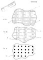
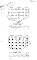
- Such template (7) which later serves also a sample carrier during milling ( Figure 3b), includes two basic references: one rectangular structure (8) capable of framing device source (4) perfectly and a square structure (9), with the via hole pitch; clearly for the latter, a suitable template (10) is required, as shown in figure 3c.
- the first phase of the process is that of producing, on the front (1) of GaAs substrate (2) the device of interest, such as a power MESFET; then to align via holes (5) on the rear (3) of the device, correspondingly to source pads (4), the following steps are taken:
- the main characteristics of the invention may be summarized in the fact that such technique, which uses conventional photolithography to align, with high recording accuracy, a predetermined structure on the rear of a sample, takes as reference the device produced on its front.
- This technique uses a suitable template onto which the substrate of interest is aligned and bonded; such template is later also used as reference to align a predetermined structure on the rear of the substrate.
- via holes can be aligned on the rear of a GaAs substrate, in perfect correspondence with the source of power MESFET devices.
- this technique does not require any peculiar equipment and furthermore, it is applicable to any type of substrate, such as Silicon, Germanium, composite semiconductors, quartz, glass, metal etc.
Landscapes
- Physics & Mathematics (AREA)
- General Physics & Mathematics (AREA)
- Exposure Of Semiconductors, Excluding Electron Or Ion Beam Exposure (AREA)
- Exposure And Positioning Against Photoresist Photosensitive Materials (AREA)
- Sampling And Sample Adjustment (AREA)
- Container, Conveyance, Adherence, Positioning, Of Wafer (AREA)
Applications Claiming Priority (2)
| Application Number | Priority Date | Filing Date | Title |
|---|---|---|---|
| IT4820586 | 1986-06-30 | ||
| IT48205/86A IT1191977B (it) | 1986-06-30 | 1986-06-30 | Tecnica per allineare con fotolitografia convenzionale una struttura sul retro di un campione con alta precisione di registrazione |
Publications (2)
| Publication Number | Publication Date |
|---|---|
| EP0252029A2 true EP0252029A2 (de) | 1988-01-07 |
| EP0252029A3 EP0252029A3 (de) | 1988-12-14 |
Family
ID=11265212
Family Applications (1)
| Application Number | Title | Priority Date | Filing Date |
|---|---|---|---|
| EP87830241A Withdrawn EP0252029A3 (de) | 1986-06-30 | 1987-06-26 | Ausrichtverfahren mittels konventioneller Photolitographie einer Struktur auf die Rückseite eines Musters mit hoher Aufnahmegenauigkeit |
Country Status (3)
| Country | Link |
|---|---|
| US (1) | US4818724A (de) |
| EP (1) | EP0252029A3 (de) |
| IT (1) | IT1191977B (de) |
Families Citing this family (14)
| Publication number | Priority date | Publication date | Assignee | Title |
|---|---|---|---|---|
| US4970578A (en) * | 1987-05-01 | 1990-11-13 | Raytheon Company | Selective backside plating of GaAs monolithic microwave integrated circuits |
| JPH023938A (ja) * | 1988-06-20 | 1990-01-09 | Mitsubishi Electric Corp | 電界効果トランジスタ |
| JPH0267731A (ja) * | 1988-09-02 | 1990-03-07 | Toshiba Corp | はんだバンプ形半導体装置とその製造方法 |
| US5139968A (en) * | 1989-03-03 | 1992-08-18 | Mitsubishi Denki Kabushiki Kaisha | Method of producing a t-shaped gate electrode |
| FR2684801B1 (fr) * | 1991-12-06 | 1997-01-24 | Picogiga Sa | Procede de realisation de composants semiconducteurs, notamment sur gaas ou inp, avec recuperation du substrat par voie chimique. |
| US5819394A (en) * | 1995-02-22 | 1998-10-13 | Transition Automation, Inc. | Method of making board matched nested support fixture |
| DE19509231C2 (de) * | 1995-03-17 | 2000-02-17 | Ibm | Verfahren zum Aufbringen einer Metallisierung auf einem Isolator und zum Öffnen von Durchgangslöchern in diesem |
| JP4465745B2 (ja) * | 1999-07-23 | 2010-05-19 | ソニー株式会社 | 半導体積層基板,半導体結晶基板および半導体素子ならびにそれらの製造方法 |
| SG121844A1 (en) * | 2002-12-20 | 2006-05-26 | Asml Netherlands Bv | Device manufacturing method |
| EP1469355B1 (de) * | 2002-12-20 | 2008-08-20 | ASML Netherlands B.V. | Verfahren zur Herstellung einer Vorrichtung |
| US7381953B1 (en) * | 2003-07-25 | 2008-06-03 | Public Service Solutions, Inc. | Infrared imaging device |
| US12440910B2 (en) | 2019-07-18 | 2025-10-14 | Transition Automation, Inc. | Paste retainer systems and methods for use in paste printing systems |
| US12162096B1 (en) | 2019-09-10 | 2024-12-10 | Transition Automation, Inc. | Squeegee blade holder with secondary blade mounting apparatus |
| US12226062B1 (en) | 2023-01-11 | 2025-02-18 | Transition Automation, Inc. | Squeegee holder with an integrated clamp bar |
Family Cites Families (12)
| Publication number | Priority date | Publication date | Assignee | Title |
|---|---|---|---|---|
| FR2013735A1 (de) * | 1968-07-05 | 1970-04-10 | Gen Electric Inf Ita | |
| US3588347A (en) * | 1969-03-13 | 1971-06-28 | Western Electric Co | Method and apparatus for aligning a mask and a substrate using infrared radiation |
| US3986196A (en) * | 1975-06-30 | 1976-10-12 | Varian Associates | Through-substrate source contact for microwave FET |
| US3984680A (en) * | 1975-10-14 | 1976-10-05 | Massachusetts Institute Of Technology | Soft X-ray mask alignment system |
| US4104099A (en) * | 1977-01-27 | 1978-08-01 | International Telephone And Telegraph Corporation | Method and apparatus for lapping or polishing materials |
| JPS54379A (en) * | 1977-05-31 | 1979-01-05 | Tsubakimoto Chain Co | Storage conveyor |
| US4309813A (en) * | 1979-12-26 | 1982-01-12 | Harris Corporation | Mask alignment scheme for laterally and totally dielectrically isolated integrated circuits |
| DE3177317T2 (de) * | 1980-04-10 | 1999-02-25 | Massachusetts Institute Of Technology, Cambridge, Mass. | Verfahren zur Herstellung von Blättern aus kristallinem Material |
| US4374915A (en) * | 1981-07-30 | 1983-02-22 | Intel Corporation | High contrast alignment marker for integrated circuit fabrication |
| US4348253A (en) * | 1981-11-12 | 1982-09-07 | Rca Corporation | Method for fabricating via holes in a semiconductor wafer |
| JPS60565A (ja) * | 1983-06-15 | 1985-01-05 | Mitsubishi Electric Corp | 分散形デ−タ処理システム |
| US4669175A (en) * | 1985-12-02 | 1987-06-02 | Honeywell Inc. | Front-to-back alignment procedure for Burrus LED's |
-
1986
- 1986-06-30 IT IT48205/86A patent/IT1191977B/it active
-
1987
- 1987-06-26 EP EP87830241A patent/EP0252029A3/de not_active Withdrawn
- 1987-06-30 US US07/068,645 patent/US4818724A/en not_active Expired - Fee Related
Also Published As
| Publication number | Publication date |
|---|---|
| IT1191977B (it) | 1988-03-31 |
| US4818724A (en) | 1989-04-04 |
| IT8648205A1 (it) | 1987-12-30 |
| EP0252029A3 (de) | 1988-12-14 |
| IT8648205A0 (it) | 1986-06-30 |
Similar Documents
| Publication | Publication Date | Title |
|---|---|---|
| EP0252029A2 (de) | Ausrichtverfahren mittels konventioneller Photolitographie einer Struktur auf die Rückseite eines Musters mit hoher Aufnahmegenauigkeit | |
| US8409971B2 (en) | Integrated multicomponent device in a semiconducting die | |
| US3956052A (en) | Recessed metallurgy for dielectric substrates | |
| KR100753741B1 (ko) | 전자 회로용의 자립 반도체 박층을 얻는 방법 | |
| US5656552A (en) | Method of making a thin conformal high-yielding multi-chip module | |
| DE102006025162B3 (de) | Flip-Chip-Bauelement und Verfahren zur Herstellung | |
| US6034405A (en) | Bonding of aluminum oxide components to silicons substrates | |
| JPH10502493A (ja) | 三次元回路装置の製造方法 | |
| JPH08335605A (ja) | フラックスレス・フリップ・チップ・ボンディングおよびその製造方法 | |
| EP0400332A3 (de) | Verfahren zur Herstellung einer mehrschichtigen Zwischenverbindungs-Leiterplattenanordnung unter Anwendung der Dünnfilmtechnik | |
| EP0231794A3 (de) | Apparat und Verfahren zur Herstellung von Metallsilicid/Silizium-Strukturen | |
| US7084047B2 (en) | Method for the production of individual monolithically integrated semiconductor circuits | |
| JPS56142633A (en) | Forming method for back electrode of semiconductor wafer | |
| JPH03126540A (ja) | 多孔性セラミック基板内の欠陥を気密シールする方法 | |
| US20020174936A1 (en) | Methods for forming recessed patterns in a multilayered ceramic package and devices produced by such methods | |
| US4890156A (en) | Multichip IC module having coplanar dice and substrate | |
| KR20010051524A (ko) | Koh 엣칭제에 의한 기질 엣칭동안 반도체 기질상에형성된 구조물 표면보호를 위한 금속필름 | |
| ES8600423A1 (es) | Procedimiento para metalizar sustratos | |
| JPH10270387A (ja) | 半導体装置の製造方法 | |
| US4792533A (en) | Coplanar die to substrate bond method | |
| JPH05109679A (ja) | 半導体装置の製造方法 | |
| JP2891488B2 (ja) | 半導体装置及びその製造方法 | |
| EP0895111A1 (de) | Verfahren zum Verbinden von Aluminiumoxid und Siliziumsubstraten | |
| Blum et al. | Multichip module substrates | |
| CN100445871C (zh) | 接合晶片的方法 |
Legal Events
| Date | Code | Title | Description |
|---|---|---|---|
| PUAI | Public reference made under article 153(3) epc to a published international application that has entered the european phase |
Free format text: ORIGINAL CODE: 0009012 |
|
| AK | Designated contracting states |
Kind code of ref document: A2 Designated state(s): DE FR GB NL SE |
|
| PUAL | Search report despatched |
Free format text: ORIGINAL CODE: 0009013 |
|
| AK | Designated contracting states |
Kind code of ref document: A3 Designated state(s): DE FR GB NL SE |
|
| 17P | Request for examination filed |
Effective date: 19890613 |
|
| STAA | Information on the status of an ep patent application or granted ep patent |
Free format text: STATUS: THE APPLICATION IS DEEMED TO BE WITHDRAWN |
|
| 18D | Application deemed to be withdrawn |
Effective date: 19920103 |
|
| RIN1 | Information on inventor provided before grant (corrected) |
Inventor name: THE OTHER INVENTORS HAVE AGREED TO WAIVE THEIR ENT Inventor name: ANTONIO, CETRONIO Inventor name: DI BONA, MAURIZIO |