EP0252029A2 - Technique for the alignment through conventional photolithography of a structure on the back of a sample with high recording accuracy - Google Patents
Technique for the alignment through conventional photolithography of a structure on the back of a sample with high recording accuracy Download PDFInfo
- Publication number
- EP0252029A2 EP0252029A2 EP87830241A EP87830241A EP0252029A2 EP 0252029 A2 EP0252029 A2 EP 0252029A2 EP 87830241 A EP87830241 A EP 87830241A EP 87830241 A EP87830241 A EP 87830241A EP 0252029 A2 EP0252029 A2 EP 0252029A2
- Authority
- EP
- European Patent Office
- Prior art keywords
- sample
- template
- technique
- substrate
- conventional photolithography
- Prior art date
- Legal status (The legal status is an assumption and is not a legal conclusion. Google has not performed a legal analysis and makes no representation as to the accuracy of the status listed.)
- Withdrawn
Links
Images

Classifications
-
- G—PHYSICS
- G03—PHOTOGRAPHY; CINEMATOGRAPHY; ANALOGOUS TECHNIQUES USING WAVES OTHER THAN OPTICAL WAVES; ELECTROGRAPHY; HOLOGRAPHY
- G03F—PHOTOMECHANICAL PRODUCTION OF TEXTURED OR PATTERNED SURFACES, e.g. FOR PRINTING, FOR PROCESSING OF SEMICONDUCTOR DEVICES; MATERIALS THEREFOR; ORIGINALS THEREFOR; APPARATUS SPECIALLY ADAPTED THEREFOR
- G03F9/00—Registration or positioning of originals, masks, frames, photographic sheets or textured or patterned surfaces, e.g. automatically
- G03F9/70—Registration or positioning of originals, masks, frames, photographic sheets or textured or patterned surfaces, e.g. automatically for microlithography
-
- G—PHYSICS
- G03—PHOTOGRAPHY; CINEMATOGRAPHY; ANALOGOUS TECHNIQUES USING WAVES OTHER THAN OPTICAL WAVES; ELECTROGRAPHY; HOLOGRAPHY
- G03F—PHOTOMECHANICAL PRODUCTION OF TEXTURED OR PATTERNED SURFACES, e.g. FOR PRINTING, FOR PROCESSING OF SEMICONDUCTOR DEVICES; MATERIALS THEREFOR; ORIGINALS THEREFOR; APPARATUS SPECIALLY ADAPTED THEREFOR
- G03F9/00—Registration or positioning of originals, masks, frames, photographic sheets or textured or patterned surfaces, e.g. automatically
-
- H—ELECTRICITY
- H01—ELECTRIC ELEMENTS
- H01L—SEMICONDUCTOR DEVICES NOT COVERED BY CLASS H10
- H01L2924/00—Indexing scheme for arrangements or methods for connecting or disconnecting semiconductor or solid-state bodies as covered by H01L24/00
- H01L2924/10—Details of semiconductor or other solid state devices to be connected
- H01L2924/1015—Shape
- H01L2924/10155—Shape being other than a cuboid
- H01L2924/10158—Shape being other than a cuboid at the passive surface
-
- H—ELECTRICITY
- H01—ELECTRIC ELEMENTS
- H01L—SEMICONDUCTOR DEVICES NOT COVERED BY CLASS H10
- H01L2924/00—Indexing scheme for arrangements or methods for connecting or disconnecting semiconductor or solid-state bodies as covered by H01L24/00
- H01L2924/10—Details of semiconductor or other solid state devices to be connected
- H01L2924/102—Material of the semiconductor or solid state bodies
- H01L2924/1025—Semiconducting materials
- H01L2924/1026—Compound semiconductors
- H01L2924/1032—III-V
- H01L2924/10329—Gallium arsenide [GaAs]
-
- Y—GENERAL TAGGING OF NEW TECHNOLOGICAL DEVELOPMENTS; GENERAL TAGGING OF CROSS-SECTIONAL TECHNOLOGIES SPANNING OVER SEVERAL SECTIONS OF THE IPC; TECHNICAL SUBJECTS COVERED BY FORMER USPC CROSS-REFERENCE ART COLLECTIONS [XRACs] AND DIGESTS
- Y10—TECHNICAL SUBJECTS COVERED BY FORMER USPC
- Y10S—TECHNICAL SUBJECTS COVERED BY FORMER USPC CROSS-REFERENCE ART COLLECTIONS [XRACs] AND DIGESTS
- Y10S148/00—Metal treatment
- Y10S148/102—Mask alignment
-
- Y—GENERAL TAGGING OF NEW TECHNOLOGICAL DEVELOPMENTS; GENERAL TAGGING OF CROSS-SECTIONAL TECHNOLOGIES SPANNING OVER SEVERAL SECTIONS OF THE IPC; TECHNICAL SUBJECTS COVERED BY FORMER USPC CROSS-REFERENCE ART COLLECTIONS [XRACs] AND DIGESTS
- Y10—TECHNICAL SUBJECTS COVERED BY FORMER USPC
- Y10S—TECHNICAL SUBJECTS COVERED BY FORMER USPC CROSS-REFERENCE ART COLLECTIONS [XRACs] AND DIGESTS
- Y10S438/00—Semiconductor device manufacturing: process
- Y10S438/928—Front and rear surface processing
-
- Y—GENERAL TAGGING OF NEW TECHNOLOGICAL DEVELOPMENTS; GENERAL TAGGING OF CROSS-SECTIONAL TECHNOLOGIES SPANNING OVER SEVERAL SECTIONS OF THE IPC; TECHNICAL SUBJECTS COVERED BY FORMER USPC CROSS-REFERENCE ART COLLECTIONS [XRACs] AND DIGESTS
- Y10—TECHNICAL SUBJECTS COVERED BY FORMER USPC
- Y10S—TECHNICAL SUBJECTS COVERED BY FORMER USPC CROSS-REFERENCE ART COLLECTIONS [XRACs] AND DIGESTS
- Y10S438/00—Semiconductor device manufacturing: process
- Y10S438/977—Thinning or removal of substrate
Definitions
- the invention takes regard for a technique through which a structure may be aligned with great recording accuracy on the rear of a sample, using conventional photolithography.
- the technique covered by the invention presented herein is based upon the use of a suitable stencil which is used,as well as in conventional terms, also as a support for the substrate of interest, that is to say, the same template provides for alignment and bonding of the substrate onto the support and also provides for the alignment of any support on the rear of the substrate itself through its own visible references on the exterior of the latter.
- the innovative phases of this invention are, essentially,those under b) and d).
- the technique presented has the advantage of not introducing further technological steps to the process.
- the great advantage of this technique is that it does not require particular equipment (a conventional aligner is all that is required) and as such it disposes of the need for costly infrared systems.
- These in fact work on the principle that many semiconductors are transparent to infrared wavelengths, so that it is possible to see through the material during alignment on the rear.
- the technique proposed has the further advantege of being applicable to any type of substrate and, up to a certain extent, this can take place indipendently of the substrate thickness.
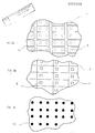
- Such template (7) which later serves also a sample carrier during milling ( Figure 3b), includes two basic references: one rectangular structure (8) capable of framing device source (4) perfectly and a square structure (9), with the via hole pitch; clearly for the latter, a suitable template (10) is required, as shown in figure 3c.
- the first phase of the process is that of producing, on the front (1) of GaAs substrate (2) the device of interest, such as a power MESFET; then to align via holes (5) on the rear (3) of the device, correspondingly to source pads (4), the following steps are taken:
- the main characteristics of the invention may be summarized in the fact that such technique, which uses conventional photolithography to align, with high recording accuracy, a predetermined structure on the rear of a sample, takes as reference the device produced on its front.
- This technique uses a suitable template onto which the substrate of interest is aligned and bonded; such template is later also used as reference to align a predetermined structure on the rear of the substrate.
- via holes can be aligned on the rear of a GaAs substrate, in perfect correspondence with the source of power MESFET devices.
- this technique does not require any peculiar equipment and furthermore, it is applicable to any type of substrate, such as Silicon, Germanium, composite semiconductors, quartz, glass, metal etc.
Abstract
Description
- The invention takes regard for a technique through which a structure may be aligned with great recording accuracy on the rear of a sample, using conventional photolithography.
- For those devices using volume (2) characteristics of the material, at times there is a need to align, on the back of sample (3), structures (4) of great recording accuracy, with the corresponding work performed on the front (1).Such technique, through adoption of conventional photolithography, gives way to structures of the type shownm with an alignment tolerance between front and rear,of ± 1 µm.
- In particular, the technique covered by the invention presented herein, is based upon the use of a suitable stencil which is used,as well as in conventional terms, also as a support for the substrate of interest, that is to say, the same template provides for alignment and bonding of the substrate onto the support and also provides for the alignment of any support on the rear of the substrate itself through its own visible references on the exterior of the latter.
- One of the various ways in which the invention's innovative process may be implemented is described, in particular to obtain,via holes on Ga As strata to ground, as shown in Figure 2, sources (4) of power MESFETS through the thickness of the material (2).
- The invention will now be described with non limiting illustrative purpose, with reference to the figures enclosed:
- Figure 1 shows the section of an hypothetical structure, built on the front and rear of a substrate in which :
- (1) sample front;
- (2) sample;
- (3) sample rear;
- (4) structure (or tooling) on the sample surfaces;
- Figure 2 shows the shematic outline of the via - holes aligned under the source pads of a power MESFET, in which:
- (5) via holes;
- (6) metal layer;
- (7) stencil;
- Figure 3a shows the tooled front surface of the sample.
- Figure 3b shows the surface of the stencil onto which the sample is bonded, where
- (8) is a rectangular structure on the sample carrier template;
- (9) is a square structure on the sample carrier template;
- (10) is the template to align the structure on the sample rear.
- Figure 3c is the surface of the template to obtain the structure on the sample rear.
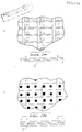
- Figure 4 shows two of the implementation phases during structure alignment on the rear of the sample;
a) template-sample-template assembly ready for alignment of the structure on the rear. - In short, the salient features of this process are the following:
- a) production of the MESFET on the front (1) of GaAs substrate (2);
- b) bonding of substrate (2) on a suitable sample carrier (7);
- c) milling of GaAs substrate (2) to reduce it to the required thrickness;
- d) alignment of the via holes (5) template on the rear (3) of the substrate correspondingly to the source pads (4);
- e) erosion of GaAs to produce via holes (4);
- f) metal coating (6) of the rear (3) to ground sources (4) of the MESFET through the volume material of substrate (2).
- The innovative phases of this invention are, essentially,those under b) and d). In fact, as the thinning of the substrate is essential for power MESFET to achieve good thermal impedance of the device, in this application the technique presented has the advantage of not introducing further technological steps to the process. However the great advantage of this technique is that it does not require particular equipment (a conventional aligner is all that is required) and as such it disposes of the need for costly infrared systems. These in fact work on the principle that many semiconductors are transparent to infrared wavelengths, so that it is possible to see through the material during alignment on the rear. Obviously, compared to infrared systems, the technique proposed has the further advantege of being applicable to any type of substrate and, up to a certain extent, this can take place indipendently of the substrate thickness.
- The details of the different production phases required to align via holes (5) on the rear (3) of a GaAs substrate correspondingly to source (4) of MESFET devices on the front (1), as already shown in Figure 2, will now be presented with reference to the schematic illustrations presented in figures 3 and 4.
- To achieve the following alignment (Figure 3a) through conventional photolythography, one must generate a template supplementary to those otherwise required by IR. Such template (7), which later serves also a sample carrier during milling (Figure 3b), includes two basic references: one rectangular structure (8) capable of framing device source (4) perfectly and a square structure (9), with the via hole pitch; clearly for the latter, a suitable template (10) is required, as shown in figure 3c.
- As mentioned above, the first phase of the process is that of producing, on the front (1) of GaAs substrate (2) the device of interest, such as a power MESFET; then to align via holes (5) on the rear (3) of the device, correspondingly to source pads (4), the following steps are taken:
- g) spread a high viscosity resist on the crome plated surface of template (7), which contains the references of the device and of the via holes (fig. 3b);
- h) spread a medium viscosity resist on the front (1) of GaAs substrate (2) equipped with MESFET devices;
- i) align with the aid of a conventional aligner, template (7) with substrate (2) so that the edges of the devices fit the rectangular structure (8) on template (7) perfectly as shown in Figure 4a;
- l) once aligned, put template (7) and substrate (2) into hard contact for about 30 seconds: this exploits the bonding characteristics of the unbaked resist to bond template (7) to substrate (2);
- m) bake the assembly at 90°C for preferably one hour to stabilize bonding. At this stage, if required, the substrate may be thinned through suitable GaAs milling using template (7) sample carrier for the miller empty chuck; if thinning of the substrate isn't required, the via holes are next aligned;
- n) with template (7) acting as carrier of assembly (2), (7) previously aligned, spread a medium viscosity resist on the rear (3) of substrate (2);
- o) bake the assembly at 90°C for about 30 minutes;
- p) align through template (10) the via holes an the rear (3) of substrate (2) using the areas external to the substrate (2) as guidelines;
- q) having performed the alignment as shown in Figure 4b, expose the resist for a predetermined time, of the order of a few seconds and develop the areas exposed.
As now the via holes have been aligned, the next steps serve only to complete the process; - r) deposit a Ni film (2000°A thick) through lift off, as template of the following etches;
- s) erode the GaAs with reactive Plasma to define the via holes;
- t) evaporate a Ni/Cr: Au (300 2000°A) film;
- u) deposit through galvanic technique a 5µ thick gold film (6)
- v) peel off substrate (2) from template (7) by wetting with hot acetone.
- The main characteristics of the invention may be summarized in the fact that such technique, which uses conventional photolithography to align, with high recording accuracy, a predetermined structure on the rear of a sample, takes as reference the device produced on its front.
- This technique uses a suitable template onto which the substrate of interest is aligned and bonded; such template is later also used as reference to align a predetermined structure on the rear of the substrate. In fact, as shown with the example given, through this technique via holes can be aligned on the rear of a GaAs substrate, in perfect correspondence with the source of power MESFET devices.
- Compared to commercially available systems which utilise an IR detector and source to see through the substrate, this technique does not require any peculiar equipment and furthermore, it is applicable to any type of substrate, such as Silicon, Germanium, composite semiconductors, quartz, glass, metal etc.
Claims (5)
Applications Claiming Priority (2)
| Application Number | Priority Date | Filing Date | Title |
|---|---|---|---|
| IT48205/86A IT1191977B (en) | 1986-06-30 | 1986-06-30 | TECHNIQUE TO ALIGN WITH CONVENTIONAL PHOTOLITHOGRAPHY A STRUCTURE ON THE BACK OF A SAMPLE WITH HIGH RECORDING PRECISION |
| IT4820586 | 1986-06-30 |
Publications (2)
| Publication Number | Publication Date |
|---|---|
| EP0252029A2 true EP0252029A2 (en) | 1988-01-07 |
| EP0252029A3 EP0252029A3 (en) | 1988-12-14 |
Family
ID=11265212
Family Applications (1)
| Application Number | Title | Priority Date | Filing Date |
|---|---|---|---|
| EP87830241A Withdrawn EP0252029A3 (en) | 1986-06-30 | 1987-06-26 | Technique for the alignment through conventional photolithography of a structure on the back of a sample with high recording accuracy |
Country Status (3)
| Country | Link |
|---|---|
| US (1) | US4818724A (en) |
| EP (1) | EP0252029A3 (en) |
| IT (1) | IT1191977B (en) |
Families Citing this family (11)
| Publication number | Priority date | Publication date | Assignee | Title |
|---|---|---|---|---|
| US4970578A (en) * | 1987-05-01 | 1990-11-13 | Raytheon Company | Selective backside plating of GaAs monolithic microwave integrated circuits |
| JPH023938A (en) * | 1988-06-20 | 1990-01-09 | Mitsubishi Electric Corp | Field effect transistor |
| JPH0267731A (en) * | 1988-09-02 | 1990-03-07 | Toshiba Corp | Solder bump type semiconductor device and manufacture thereof |
| US5139968A (en) * | 1989-03-03 | 1992-08-18 | Mitsubishi Denki Kabushiki Kaisha | Method of producing a t-shaped gate electrode |
| FR2684801B1 (en) * | 1991-12-06 | 1997-01-24 | Picogiga Sa | PROCESS FOR PRODUCING SEMICONDUCTOR COMPONENTS, ESPECIALLY ON GAAS OR INP, WITH CHEMICAL RECOVERY OF THE SUBSTRATE. |
| US5819394A (en) * | 1995-02-22 | 1998-10-13 | Transition Automation, Inc. | Method of making board matched nested support fixture |
| DE19509231C2 (en) * | 1995-03-17 | 2000-02-17 | Ibm | Method of applying a metallization to an insulator and opening through holes in it |
| JP4465745B2 (en) * | 1999-07-23 | 2010-05-19 | ソニー株式会社 | Semiconductor laminated substrate, semiconductor crystal substrate, semiconductor element, and manufacturing method thereof |
| SG121844A1 (en) * | 2002-12-20 | 2006-05-26 | Asml Netherlands Bv | Device manufacturing method |
| EP1469355B1 (en) * | 2002-12-20 | 2008-08-20 | ASML Netherlands B.V. | Device manufacturing method |
| US7381953B1 (en) * | 2003-07-25 | 2008-06-03 | Public Service Solutions, Inc. | Infrared imaging device |
Citations (1)
| Publication number | Priority date | Publication date | Assignee | Title |
|---|---|---|---|---|
| US3588347A (en) * | 1969-03-13 | 1971-06-28 | Western Electric Co | Method and apparatus for aligning a mask and a substrate using infrared radiation |
Family Cites Families (11)
| Publication number | Priority date | Publication date | Assignee | Title |
|---|---|---|---|---|
| FR2013735A1 (en) * | 1968-07-05 | 1970-04-10 | Gen Electric Inf Ita | |
| US3986196A (en) * | 1975-06-30 | 1976-10-12 | Varian Associates | Through-substrate source contact for microwave FET |
| US3984680A (en) * | 1975-10-14 | 1976-10-05 | Massachusetts Institute Of Technology | Soft X-ray mask alignment system |
| US4104099A (en) * | 1977-01-27 | 1978-08-01 | International Telephone And Telegraph Corporation | Method and apparatus for lapping or polishing materials |
| JPS54379A (en) * | 1977-05-31 | 1979-01-05 | Tsubakimoto Chain Co | Storage conveyor |
| US4309813A (en) * | 1979-12-26 | 1982-01-12 | Harris Corporation | Mask alignment scheme for laterally and totally dielectrically isolated integrated circuits |
| EP0193830A3 (en) * | 1980-04-10 | 1986-10-01 | Massachusetts Institute Of Technology | Solar cell device incorporating plural constituent solar cells |
| US4374915A (en) * | 1981-07-30 | 1983-02-22 | Intel Corporation | High contrast alignment marker for integrated circuit fabrication |
| US4348253A (en) * | 1981-11-12 | 1982-09-07 | Rca Corporation | Method for fabricating via holes in a semiconductor wafer |
| JPS60565A (en) * | 1983-06-15 | 1985-01-05 | Mitsubishi Electric Corp | Distributed data processing system |
| US4669175A (en) * | 1985-12-02 | 1987-06-02 | Honeywell Inc. | Front-to-back alignment procedure for Burrus LED's |
-
1986
- 1986-06-30 IT IT48205/86A patent/IT1191977B/en active
-
1987
- 1987-06-26 EP EP87830241A patent/EP0252029A3/en not_active Withdrawn
- 1987-06-30 US US07/068,645 patent/US4818724A/en not_active Expired - Fee Related
Patent Citations (1)
| Publication number | Priority date | Publication date | Assignee | Title |
|---|---|---|---|---|
| US3588347A (en) * | 1969-03-13 | 1971-06-28 | Western Electric Co | Method and apparatus for aligning a mask and a substrate using infrared radiation |
Non-Patent Citations (2)
| Title |
|---|
| SOLID STATE TECHNOLOGY, vol. 21, no. 8, August 1978, pages 55-60; R.A. HEINZ et al.: "Double-sided photolithography" * |
| SOLID STATE TECHNOLOGY, vol. 22, no. 2, February 1979, pages 57-60; R.L. MADDOX: "Advances in double sided wafer processing" * |
Also Published As
| Publication number | Publication date |
|---|---|
| IT1191977B (en) | 1988-03-31 |
| IT8648205A0 (en) | 1986-06-30 |
| US4818724A (en) | 1989-04-04 |
| EP0252029A3 (en) | 1988-12-14 |
Similar Documents
| Publication | Publication Date | Title |
|---|---|---|
| EP0252029A2 (en) | Technique for the alignment through conventional photolithography of a structure on the back of a sample with high recording accuracy | |
| US8409971B2 (en) | Integrated multicomponent device in a semiconducting die | |
| US3956052A (en) | Recessed metallurgy for dielectric substrates | |
| US6746819B1 (en) | Use of polyimide for adhesive layers, lithographic method for producing microcomponents and method for producing composite material | |
| US5656552A (en) | Method of making a thin conformal high-yielding multi-chip module | |
| WO2004008486A3 (en) | Wafer bonding of thinned electronic materials and circuits to high performance substrates | |
| JPH10502493A (en) | Manufacturing method of three-dimensional circuit device | |
| EP0814509A3 (en) | Method for making a substrate structure with improved heat dissipation | |
| DE102016216918A1 (en) | Manufacturing method for a micromechanical device with a tilted optical window and corresponding micromechanical device | |
| EP0231794A3 (en) | Method and apparatus for forming metal silicide/silicon structures | |
| US7084047B2 (en) | Method for the production of individual monolithically integrated semiconductor circuits | |
| WO1990013391A3 (en) | Joining method | |
| JPH0992602A (en) | Mask structure and production thereof | |
| US4890156A (en) | Multichip IC module having coplanar dice and substrate | |
| KR20010051524A (en) | Metal film protection of the surface of a structure formed on a semiconductor substrate during etching of the substrate by a koh etchant | |
| ES8600423A1 (en) | Process for obtaining metallized surface using electron beam curing. | |
| JPH03126540A (en) | Method for airtight-sealing defect in porous ceramic substrate | |
| GB2156593A (en) | Through hole interconnections | |
| US4792533A (en) | Coplanar die to substrate bond method | |
| JPH10270387A (en) | Manufacture of semiconductor device | |
| WO2002096640A1 (en) | Recessed patterns in a multilayered ceramic package | |
| Blum et al. | Multichip module substrates | |
| JP2891488B2 (en) | Semiconductor device and manufacturing method thereof | |
| EP0895111A1 (en) | Bonding of aluminum oxide components to silicon substrates | |
| US4815208A (en) | Method of joining substrates for planar electrical interconnections of hybrid circuits |
Legal Events
| Date | Code | Title | Description |
|---|---|---|---|
| PUAI | Public reference made under article 153(3) epc to a published international application that has entered the european phase |
Free format text: ORIGINAL CODE: 0009012 |
|
| AK | Designated contracting states |
Kind code of ref document: A2 Designated state(s): DE FR GB NL SE |
|
| PUAL | Search report despatched |
Free format text: ORIGINAL CODE: 0009013 |
|
| AK | Designated contracting states |
Kind code of ref document: A3 Designated state(s): DE FR GB NL SE |
|
| 17P | Request for examination filed |
Effective date: 19890613 |
|
| STAA | Information on the status of an ep patent application or granted ep patent |
Free format text: STATUS: THE APPLICATION IS DEEMED TO BE WITHDRAWN |
|
| 18D | Application deemed to be withdrawn |
Effective date: 19920103 |
|
| RIN1 | Information on inventor provided before grant (corrected) |
Inventor name: THE OTHER INVENTORS HAVE AGREED TO WAIVE THEIR ENT Inventor name: ANTONIO, CETRONIO Inventor name: DI BONA, MAURIZIO |