EP0251007B1 - Rufempfänger mit geräuschimmuner Überprüfungsschaltung zur Abschaltung des Batterie-Schonbetriebes - Google Patents
Rufempfänger mit geräuschimmuner Überprüfungsschaltung zur Abschaltung des Batterie-Schonbetriebes Download PDFInfo
- Publication number
- EP0251007B1 EP0251007B1 EP87108582A EP87108582A EP0251007B1 EP 0251007 B1 EP0251007 B1 EP 0251007B1 EP 87108582 A EP87108582 A EP 87108582A EP 87108582 A EP87108582 A EP 87108582A EP 0251007 B1 EP0251007 B1 EP 0251007B1
- Authority
- EP
- European Patent Office
- Prior art keywords
- detector
- preamble
- pulse
- counter
- address
- Prior art date
- Legal status (The legal status is an assumption and is not a legal conclusion. Google has not performed a legal analysis and makes no representation as to the accuracy of the status listed.)
- Expired - Lifetime
Links
- 238000012795 verification Methods 0.000 title description 17
- 230000007704 transition Effects 0.000 claims description 18
- 230000004044 response Effects 0.000 claims description 15
- 238000011084 recovery Methods 0.000 claims description 7
- 238000001514 detection method Methods 0.000 claims description 6
- 230000000737 periodic effect Effects 0.000 claims description 4
- 238000011156 evaluation Methods 0.000 claims 3
- 238000010586 diagram Methods 0.000 description 5
- 230000000295 complement effect Effects 0.000 description 2
- 230000036039 immunity Effects 0.000 description 2
- 230000001360 synchronised effect Effects 0.000 description 2
- 230000005540 biological transmission Effects 0.000 description 1
- 238000012986 modification Methods 0.000 description 1
- 230000004048 modification Effects 0.000 description 1
- 238000012544 monitoring process Methods 0.000 description 1
- 238000001208 nuclear magnetic resonance pulse sequence Methods 0.000 description 1
Images


Classifications
-
- H—ELECTRICITY
- H04—ELECTRIC COMMUNICATION TECHNIQUE
- H04B—TRANSMISSION
- H04B1/00—Details of transmission systems, not covered by a single one of groups H04B3/00 - H04B13/00; Details of transmission systems not characterised by the medium used for transmission
- H04B1/06—Receivers
- H04B1/16—Circuits
- H04B1/1607—Supply circuits
- H04B1/1615—Switching on; Switching off, e.g. remotely
-
- H—ELECTRICITY
- H04—ELECTRIC COMMUNICATION TECHNIQUE
- H04W—WIRELESS COMMUNICATION NETWORKS
- H04W52/00—Power management, e.g. Transmission Power Control [TPC] or power classes
- H04W52/02—Power saving arrangements
- H04W52/0209—Power saving arrangements in terminal devices
- H04W52/0225—Power saving arrangements in terminal devices using monitoring of external events, e.g. the presence of a signal
- H04W52/0229—Power saving arrangements in terminal devices using monitoring of external events, e.g. the presence of a signal where the received signal is a wanted signal
-
- H—ELECTRICITY
- H04—ELECTRIC COMMUNICATION TECHNIQUE
- H04W—WIRELESS COMMUNICATION NETWORKS
- H04W52/00—Power management, e.g. Transmission Power Control [TPC] or power classes
- H04W52/02—Power saving arrangements
- H04W52/0209—Power saving arrangements in terminal devices
- H04W52/0261—Power saving arrangements in terminal devices managing power supply demand, e.g. depending on battery level
- H04W52/0274—Power saving arrangements in terminal devices managing power supply demand, e.g. depending on battery level by switching on or off the equipment or parts thereof
- H04W52/028—Power saving arrangements in terminal devices managing power supply demand, e.g. depending on battery level by switching on or off the equipment or parts thereof switching on or off only a part of the equipment circuit blocks
- H04W52/0283—Power saving arrangements in terminal devices managing power supply demand, e.g. depending on battery level by switching on or off the equipment or parts thereof switching on or off only a part of the equipment circuit blocks with sequential power up or power down of successive circuit blocks, e.g. switching on the local oscillator before RF or mixer stages
-
- H—ELECTRICITY
- H04—ELECTRIC COMMUNICATION TECHNIQUE
- H04W—WIRELESS COMMUNICATION NETWORKS
- H04W88/00—Devices specially adapted for wireless communication networks, e.g. terminals, base stations or access point devices
- H04W88/02—Terminal devices
- H04W88/022—Selective call receivers
-
- Y—GENERAL TAGGING OF NEW TECHNOLOGICAL DEVELOPMENTS; GENERAL TAGGING OF CROSS-SECTIONAL TECHNOLOGIES SPANNING OVER SEVERAL SECTIONS OF THE IPC; TECHNICAL SUBJECTS COVERED BY FORMER USPC CROSS-REFERENCE ART COLLECTIONS [XRACs] AND DIGESTS
- Y02—TECHNOLOGIES OR APPLICATIONS FOR MITIGATION OR ADAPTATION AGAINST CLIMATE CHANGE
- Y02D—CLIMATE CHANGE MITIGATION TECHNOLOGIES IN INFORMATION AND COMMUNICATION TECHNOLOGIES [ICT], I.E. INFORMATION AND COMMUNICATION TECHNOLOGIES AIMING AT THE REDUCTION OF THEIR OWN ENERGY USE
- Y02D30/00—Reducing energy consumption in communication networks
- Y02D30/70—Reducing energy consumption in communication networks in wireless communication networks
Definitions
- the present invention relates to a selective calling radio paging receiver in which the high power drain unit is rendered active at periodic intervals for power savings purposes and more specifically to a radio paging receiver having a verification circuit that verifies the validity of a received digital signal in the event of a loss or corruption of a preamble.
- the high power drain unit is rendered active for a duration sufficient to permit the receiver to search for a preamble that precedes a subsequent digital signal and rendered inactive for an interval much longer than the active duration if the preamble is not detected. If the preamble is detected, the battery saving operation is disabled to permit the receiver to search for a synchronization codeword to establish word synchronization and for a match between a received address and the user's address to energize a tone generator for alerting the user.
- the receiver recognizes it as an absence of paging signal and the subsequent signal will be lost.
- a power saving radio pager overcomes this problem by monitoring the bit rate of a digital signal received during its short active period and verifying it as a valid signal if it has a predetermined bit rate.
- the pager employs a counter for counting binary level transitions of received digital pulses and a noise detector that clears the counter to the initial value whenever a noise impulse occurs in the received bit sequence.
- the noise component must be excluded from the count if it is desired to ensure a high degree of verification, the occurrence of a single noise impulse near the end of a count sequence would nullify the count which could be used as a valid indication of a paging signal. Therefore, the prior art paging receiver is likely to be affected by noise impulses which can be tolerated for most practical applications.
- EP-A-0 095 750 discloses a preamble detector for detecting the preamble of a predetermined bit-sequence. Because of the pre-known bit-sequence, the decision steps determine the logic value of the received bit in order to record an error bit as a count.
- the pulse integrator/detector of JP-A-194 627/85 comprises counters which are incremented by locally generated clock pulses without detecting transition pulses by an edge detector.
- the noise-immune verification circuit is enabled during the active period of the receiver and includes a window pulse generator for generating a window pulse in synchronism with a recovered clock pulse so that each binary level transition of a received digital pulse is time coincident with each window pulse. If noise occurs in the received signal, binary level transitions are noncoincident with window pulses. A first count of the time-coincident binary level transitions and a second count of the noncoincident binary level transitions are taken and compared against each other for verifying the signal if the first count exceeds the second count.
- the selective calling radio paging receiver receives a digital bit stream containing a preamble followed by a series of blocks each having a synchronization codeword and a series of address codewords.
- a battery saving controller activates the high power drain unit of the receiver at periodic intervals.
- the high power drain unit is continuously activated to permit a sync detector to search for a synchronization codeword, and then an address detector to search for a match between an address codeword and the user's address.
- First and second counters are enabled during the active period of the receiver to respectively provide the first and second counts and compared against each other for verification of the received signal.
- the high power drain unit is continuously activated to permit the sync detector to search for a synchronization codeword, and then the address detector to search for a match between an address codeword and the user's address.
- the selective calling radio pager of the present invention is shown in Fig. 1.
- the pager includes a front end, or a radio-frequency section 2 which amplifies and demodulates a digitally modulated paging signal received by antenna 1 and applies the demodulated digital pulse signal to an edge detector 3, a preamble detector 5, a sync detector 8 and an address detector 9.
- a transition pulse is generated at the output of edge detector 3 in response to each of the leading and trailing edge transitions of each digital pulse and fed to a clock recovery and window pulse generation circuit 6 and a verification circuit 7.
- Clock recovery and window pulse generation circuit 6 recovers clock timing from the incoming bit stream and supplies recovered clock pulses to the preamble detector 5, verification circuit 7, sync detector 8 and address detector 9 and further to an address memory 10.
- the paging signal is a code sequence preferably formatted according to the standards specified by The British Post Office Code Standardisation Advisory Group (known as POCSAG) and transmitted from a central calling station.
- Each transmission starts with a preamble to permit the pager to attain bit synchronization and to prepare it to acquire word synchrozation.
- the preamble is a pattern of reversals of binary 1's and 0's for a period of 576 bits.
- Codewords are transmitted in batches each of which comprises a synchronization codeword to permit the pager to establish word synchronization, the synchronization codeword being followed by eight frames each containing 2 codewords of 32 bits each. The frames are numbered 0 to 7 and the pager population is similarly divided into 8 groups. Each pager is allocated to one of the 8 frames in which an address codeword of the pager is transmitted. In the absence of an address codeword, an idle codeword is transmitted.
- a battery saving controller 13 which is essentially constructed of a counter and logic circuit in a well known manner, is responsive to clock pulses from clock source 4 to normally generate a periodic power control pulse having a period of 32 bits of the incoming signal (equivalent to the duration of each codeword) at synchronization intervals.
- This power control pulse activates a power switch 15 to feed power from battery 16 to the high power drain unit, i.e., the front end 2.
- the radio pager is thus periodically rendered active for the duration of a codeword to permit the preamble detector 5 to detect a preamble and remains inactive for a period of 15 codewords for power saving purposes. If a preamble is detected, the preamble detector 5 produces an output which is applied through an OR gate 14 to the battery saving controller 13.
- the verification circuit 7 cooperates with the clock recovery and window pulse generation circuit 6 to determine whether the incoming signal is valid. If it is, the verification cicuit 7 supplies an output through OR gate 14 to the battery saving controller 13. In response to a signal from OR gate 14, the battery saving controller 13 enables the sync detector 8 to search for a synchronization codeword, and whereupon the address detector 9 is allowed to search for a match between a received address codeword and a user's unique codeword stored in the address memory 10, which is implemented by a programmable read-only memory. If there is a match, the address detector 9 will cause a tone generator 11 to drive a loudspeaker 12 to alert the user of the reception of a paging signal.
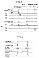
- battery saving controller 13 supplies control pulses C1, C2 and C3 to the verification circuit 7, sync detector 8 and address detector 9, respectively, as shown in Fig. 2.
- a control pulse C1 is supplied to the verification circuit 7 as shown in part (a) of Fig. 2 to permit the preamble detector 5 to search for a preamble.
- the battery saving controller 13 holds its output at high level to disable the subsequent battery saving operation, terminates the generation of a subsequent control pulse C1 and applies a second control pulse C2 to the sync detector 8 to permit it to search for a subsequent synchronization codeword.
- a third control pulse C3 is applied to the address detector 9 and memory 10 to allow bit-by-bit comparison to be made by address detector 9 to search for a match between the user's address and a received address codeword. If there is one, the battery saving disablement is continued, and if there is none, battery saving operation is resumed after a time-out action. On the other hand, if a preamble is not detected in a valid incoming signal during a given active period and an output signal is generated by the verification circuit 7 during a subsequent active period, the subsequent battery saving operation is disabled and a control pulse C2 is applied to the sync detector 8 to allow it to search for a subsequent synchronization codeword as shown in part (b) of Fig. 2. When this synchronization codeword is detected, a control pulse C3 is applied to address detector 9 and address memory 10 to allow detection of a match between the user's address and a received address.
- the clock recovery and window pulse generation circuit 6 comprises a phase detector 20, a programmable counter or variable frequency divider 21, a divide-by-2 counter 22 and a window pulse generator 23.
- Phase detector 20 detects the phase difference between the output of edge detector 3 and the output of divide-by-2 counter 22 and generates an in-phase signal by setting the dividing factor of the frequency divider 21 to N when there is a phase match between the two signals.
- Phase detector 20 generates a phase advance command signal by resetting the dividing factor to N-1 when the transition pulse lags behind the output of divide-by-2 counter 22 or a phase retard command signal by resetting it to N+1 when the transition pulse advances with respect to the counter 22 output.
- Frequency divider 21 provides a count of the locally generated clock pulses and generates an output when the count equals the dividing factor N.
- Divide-by-2 counter 22 halves the frequency of the output of frequency divider 21.
- Window pulse generator 23 derives a window pulse from the output of divide-by-2 counter 22 and from the output of an appropriate bit position of the frequency divider 21. Due to the phase-locked loop, the divide-by-2 counter 22 is synchronized with the incoming bit stream to recover its clock timing and the window pulse is synchronized with the recovered clock pulse (Fig. 4). Therefore, the output of edge detector 3 occurs within the period of each window pulse if the incoming bit stream is a valid paging signal and occurs outside of the window pulse when the incoming signal contains a noise impulse or jitter.
- Verification circuit 7 includes a counter 30 that counts transition pulses from edge detector 3 in response to the first control pulse C1 from the battery saving controller 13 and supplies a reset signal to counters 31 and 33 when the count reaches a prescribed value, typically eight.
- the output of window pulse generator 23 is applied to an AND gate 32 on the one hand and by way of an inverter 35 to an AND gate 34 on the other. Therefore, AND gate 32 is enabled during the presence of a window pulse to pass the output of edge detector 3 to counter 31 and AND gate 34 is enabled during the interval between successive window pulses to pass the edge detector output to counter 33.
- counter 31 provides a count of transition pulses occurring within the window pulses and counter 33 provides a count of transition pulses that occur outside the window pulses.
- the counts provided by counters 31 and 33 are compared against each other by a digital comparator 36 so that it generates a logical-1 output when there is a larger number of transition pulses occurring within the window pulses than the number of those occurring outside the window pulses.
- the output of comparator 36 is applied to the data input of a D flip-flop 37.
- a 32-bit counter 38 is connected to the output of divide-by-2 counter 22. Counter 38 is reset in response to the control pulse C1 to start counting the recovered clock pulse to measure the duration in which the front end 2 is active and at the end of the count it supplies an output to the clock input of flip-flop 37 to latch the output of comparator 36.
- an incoming bit stream can be treated as a valid paging signal, a greater number of counts will be stored in counter 31 during the prescribed period than the counts stored in counter 33 and a binary 1 is latched in the flip-flop 37. Otherwise, a greater number of counts will be stored in counter 33 than those stored in counter 31 and a binary 0 is latched in the flip-flop 37.
- the output of flip-flop 37 is connected through OR gate 14 to the power saving circuit 13. If binary 1 is latched in flip-flop 37, the power saving circuit 13 keeps its output at high level to maintain the front end 2 in the active state. Therefore, the battery saving operation can be disabled in response to the reception of a valid incoming signal even though the receiver fails to detect a preamble. As described above, the receiver proceeds to search for a subsequent synchronization codeword to attain word synchronization to permit the address detector 9 to search for a match between a received address and the user's unique codeword.
- the verification circuit 7 provides a valid indication of the incoming signal with a higher degree of immunity to noise than the degree of immunity of the aforesaid United States patent.
- Preamble detector 5 comprises a 32-bit shift register 40 having a data input coupled to the output of front end 2 and a clock input connected to the output of divide-by-2 counter 22 to shift the incoming digital pulses along the shift register stages in response to the recovered clock timing.
- a decoding logic 41 is formed by a plurality of NOT circuits and an AND gate having inputs coupled directly or by way of the NOT circuits to the shift register stages to form a combination of binary states corresponding to the bit pattern of the preamble to generate an output when the pattern of bits clocked into shift register 40 coincides with the bit pattern of the decoding logic 41.
- Shift register 40 is reset to all zero's in response to the output of the decoding logic 41.
- Sync detector 8 is similarly constructed to the preamble detector 5 with the exception that a decoding logic 43 defines the bit pattern of the synchronization codeword of the paging signal. Shift register 42 is reset in response to the second control pulse C2 which is supplied from the battery saving controller 13 either when a preamble is detected by preamble detector 5 or a valid indication of a received bit stream is given by verification circuit 7. Decoding logic 43 generates an output when the shift register 42 is loaded with bits that coincide with the sync pattern.
- Address detector 9 comprises an exclusive-OR gate 44 which combines the outputs of front end 2 and address memory 10 and applies its output to a first input of an AND gate 45 to the second input of which is applied the recovered clock pulse from the divide-by-2 counter 22.
- AND gate 45 supplies an output to the clock input of a D flip-flop 46 of which the data input is connected to a positive dc supply.
- the complementary Q output of flip-flop 46 is connected to the data input of a D flip-flop 47.
- a 32-bit counter 48 which is reset by the control pulse C3 from the battery saving controller 13, counts the recovered clock pulse and supplies a first output to the reset inputs of flip-flops 46 and 47 in response to the first bit of a series of 32 clock pulses which corresponds to the beginning of an address codeword and a second output to the clock input of flip-flop 47 in response to the last bit of the clock pulse sequence which corresponds to the end of the codeword.
- exclusive-OR gate 44 makes a bit-by-bit comparison of its inputs so that it generates a binary 0 when a match occurs therebetween and a binary 1 when no match occurs.
- the binary 1's (mismatch) from the exclusive-OR gate 44 are passed to the clock input of flip-flop 46 to drive its complementary Q output to a logical 0 level, which is latched in the flip-flop 47. If there is a bit-by-bit mismatch between the inputs at the exclusive-OR gate 44, a binary 0 is latched in the flip-flop 47, and therefore, if coincidence exists between all the 32 bits of the compared signals, a binary 1 is latched in the flip-flop 47 to drive the tone generator 11.
Landscapes
- Engineering & Computer Science (AREA)
- Computer Networks & Wireless Communication (AREA)
- Signal Processing (AREA)
- Mobile Radio Communication Systems (AREA)
Claims (3)
- Selektiv abrufender Funkrufempfänger mita) einem Präambeldetektor (5) zum Feststellen einer Präambel,b) einem Adreßdetektor (9) zum Feststellen einer Übereinstimmung zwischen einer in einem empfangenen Bitstrom enthaltenen Adresse und der Adresse des Empfängers nach Feststellung der Präambel,c) einer batterieschonenden Einrichtung (13) zum Unterbrechen der Stromversorgung zu einer leistungsaufnehmenden Einheit des Empfängers in regelmäßigen Zeitabständen,d) einer taktrückgewinnenden Einrichtung (6) zum Rückgewinnen von Taktimpulsen aus dem Bitstrom sowiee) einer Rauschbewertungs-Schaltung zum Deaktivieren der batterieschonenden Einrichtung, wenn das Rauschen des empfangenen Bitstroms einen unzulässigen Wert hat, wobei die Rauschbewertungs-Schaltung einen ersten und zweiten Zähler (31, 33) zum Zählen von Impulsen während aufeinanderfolgender Perioden und zum Bewerten des Rauschens anhand einer Differenz zwischen den jeweiligen, durch die Zähler (31, 33) ermittelten Zählungen aufweist;dadurch gekennzeichnet, daßf) die Rauschbewertungs-Schaltung einen Flankendetektor (3) zum Feststellen der Vorder- und Rückflanke jedes Impulses im Bitstrom und zum Erzeugen eines Übergangsimpulses als Reaktion auf die Feststellung jeder Vorder- und Rückflanke sowie einen Fensterimpulsgenerator (23) zum Erzeugen eines Fensterimpulses als Reaktion auf jeden rückgewonnenen Taktimpuls aufweist,g) der erste Zähler (31) den Übergangsimpuls innerhalb des Fensterimpulses zählt und der zweite Zähler (33) den Übergangsimpuls außerhalb des Fensterimpulses zählt, sowieh) ein Komparator (36) vorgesehen ist zum vergleichen des Ausgangssignals des ersten Zählers (31) mit dem Ausgangssignal des zweiten Zählers (33) und zum Anlegen eines Deaktivierungs-Befehlssignals an der batterieschonenden Einrichtung (13), wenn das erste Ausgangssignal größer als das letzte ist.
- Selektiv abrufender Funkrufempfänger nach Anspruch 1, dadurch gekennzeichnet, daß ein dritter Zähler (30) vorgesehen ist zum Zählen des Übergangsimpulses und zum Erzeugen eines Ausgangssignals, wenn die Zählung einen vorbestimmten Wert erreicht, und zum Anlegen des Ausgangssignals am ersten und zweiten Zähler (31, 33) als Rücksetzsignal.
- Selektiv abrufender Funkrufempfänger nach Anspruch 1 oder 2, dadurch gekennzeichnet, daß ein Synchronisationsdetektor (8) vorgesehen ist zum Feststellen eines im empfangenen Bitstrom enthaltenen Synchronisations-Codes als Reaktion auf die Feststellung einer Präambel durch den Präambeldetektor (5) oder als Reaktion auf das durch den Komparator (36) erzeugte Deaktivierungs-Befehlssignal, und der Adreßdetektor (9) auf die Feststellung des Synchronisations-Codes durch den Synchronisationsdetektor (8) zum Feststellen der Übereinstimmung reagiert.
Applications Claiming Priority (2)
| Application Number | Priority Date | Filing Date | Title |
|---|---|---|---|
| JP61140305A JPH0656976B2 (ja) | 1986-06-18 | 1986-06-18 | 個別選択呼出し受信機 |
| JP140305/86 | 1986-06-18 |
Publications (3)
| Publication Number | Publication Date |
|---|---|
| EP0251007A2 EP0251007A2 (de) | 1988-01-07 |
| EP0251007A3 EP0251007A3 (en) | 1989-08-02 |
| EP0251007B1 true EP0251007B1 (de) | 1993-04-21 |
Family
ID=15265696
Family Applications (1)
| Application Number | Title | Priority Date | Filing Date |
|---|---|---|---|
| EP87108582A Expired - Lifetime EP0251007B1 (de) | 1986-06-18 | 1987-06-15 | Rufempfänger mit geräuschimmuner Überprüfungsschaltung zur Abschaltung des Batterie-Schonbetriebes |
Country Status (8)
| Country | Link |
|---|---|
| US (1) | US4837854A (de) |
| EP (1) | EP0251007B1 (de) |
| JP (1) | JPH0656976B2 (de) |
| KR (1) | KR910000303B1 (de) |
| AU (1) | AU596547B2 (de) |
| CA (1) | CA1307324C (de) |
| DE (1) | DE3785491T2 (de) |
| HK (1) | HK140093A (de) |
Families Citing this family (30)
| Publication number | Priority date | Publication date | Assignee | Title |
|---|---|---|---|---|
| US5204656A (en) * | 1987-07-10 | 1993-04-20 | U. S. Philips Corporation | Paging receiver with power supply divider |
| DE3722799C2 (de) * | 1987-07-10 | 1998-02-19 | Koninkl Philips Electronics Nv | Mobilstation mit einem Empfangsteil |
| JPH01190054A (ja) * | 1988-01-25 | 1989-07-31 | Man Design Kk | 受信機 |
| EP0347166A3 (de) * | 1988-06-14 | 1991-11-06 | Kabushiki Kaisha Toshiba | Verfahren und Einrichtung zur Verminderung des Energieverbrauchs in einem Funkübertragungsgerät |
| US5203020A (en) * | 1988-06-14 | 1993-04-13 | Kabushiki Kaisha Toshiba | Method and apparatus for reducing power consumption in a radio telecommunication apparatus |
| US5227777A (en) * | 1988-12-06 | 1993-07-13 | Nec Corporation | Radio paging receiver for intermittently receiving a paging signal transmitted on different phases of a clock |
| US4928086A (en) * | 1989-01-30 | 1990-05-22 | Motorola, Inc. | Pager receiver having a common timer circuit for both sequential lock-out and out-of-range |
| US5206885A (en) * | 1989-02-06 | 1993-04-27 | Motorola, Inc. | Selective call receiver with fast bit synchronizer |
| US5095498A (en) * | 1989-02-06 | 1992-03-10 | Motorola, Inc. | Bit synchronizer |
| US4961073A (en) * | 1989-02-27 | 1990-10-02 | Motorola, Inc. | Battery saving apparatus and method providing optimum synchronization codeword detection |
| US5032835A (en) * | 1989-04-24 | 1991-07-16 | Motorola, Inc. | Out of range indication for radio receivers |
| DE59009063D1 (de) * | 1989-12-18 | 1995-06-14 | Siemens Ag | Empfänger für ein digitales Zusatzsignal in einem digitalen Übertragungssystem. |
| US5140702A (en) * | 1990-06-05 | 1992-08-18 | Motorola, Inc. | Time based signal detector for operating in a presence search mode and absence search mode during peak times and off peak times |
| CA2094366C (en) * | 1992-04-20 | 1999-04-13 | Hiroyasu Kuramatsu | Paging receiver having data speed detector for continuing address receiving mode |
| CH685225B5 (fr) * | 1992-05-27 | 1995-11-15 | Ebauchesfabrik Eta Ag | Recepteur d'appel local a faible consommation d'energie. |
| JPH0832087B2 (ja) * | 1993-05-14 | 1996-03-27 | 日本電気株式会社 | 無線選択呼び出し信号受信機 |
| US5533039A (en) * | 1993-09-22 | 1996-07-02 | Storage Technology Corporation | Fault tolerant fiber optic protocol for determining beginning of data |
| US5563910A (en) * | 1993-11-12 | 1996-10-08 | Motorola, Inc. | Recursive baud rate detection method and apparatus |
| US5542117A (en) * | 1994-06-03 | 1996-07-30 | Motorola, Inc. | Method and apparatus for batery saving in a communication receiver |
| GB2297884B (en) * | 1995-02-07 | 1999-05-26 | Nokia Mobile Phones Ltd | Radio telephone |
| US6005885A (en) * | 1995-12-12 | 1999-12-21 | Intermec Ip Corp. | Methodology for discontinuous radio reception utilizing embedded frame length words |
| KR970060736A (ko) * | 1996-01-29 | 1997-08-12 | 김광호 | 무선 호출신호 수신방법 |
| US5793174A (en) * | 1996-09-06 | 1998-08-11 | Hunter Douglas Inc. | Electrically powered window covering assembly |
| US6075807A (en) * | 1997-03-25 | 2000-06-13 | Intermec Ip Corp. | Windowed digital matched filter circuit for power reduction in battery-powered CDMA radios |
| US6009119A (en) * | 1997-03-25 | 1999-12-28 | Intermec Ip Corp. | Adaptive power leveling of an RF transceiver utilizing information stored in non-volatile memory |
| KR100267855B1 (ko) * | 1997-12-26 | 2000-10-16 | 윤종용 | 무선호출수신기의 비규격 수신신호 처리장치 및 방법 |
| JP2001127728A (ja) * | 1999-10-29 | 2001-05-11 | Oki Electric Ind Co Ltd | 受信回路 |
| TWI309939B (en) * | 2006-01-06 | 2009-05-11 | Princeton Technology Corp | Packet preamble search method and device thereof |
| US20080130815A1 (en) * | 2006-12-05 | 2008-06-05 | Kumar S Reji | Selective tracking of serial communication link data |
| FR2959580A1 (fr) * | 2010-05-03 | 2011-11-04 | St Microelectronics Rousset | Circuit et procede de detection d'une attaque par injection de fautes |
Family Cites Families (8)
| Publication number | Priority date | Publication date | Assignee | Title |
|---|---|---|---|---|
| US3851251A (en) * | 1971-10-25 | 1974-11-26 | Martin Marietta Corp | Receiver method and apparatus |
| US4419765A (en) * | 1979-10-12 | 1983-12-06 | Keith H. Wycoff | Signal absence detector |
| JPS56136050A (en) * | 1980-03-28 | 1981-10-23 | Nec Corp | Individual selective call reception system |
| GB2105500B (en) * | 1981-06-16 | 1985-01-23 | Motorola Ltd | Data operated squelch |
| GB2103402B (en) * | 1981-07-27 | 1984-09-05 | Standard Telephones Cables Ltd | Synchronisation of digital radio pager |
| JPS58188943A (ja) * | 1982-04-14 | 1983-11-04 | Nec Corp | 無線選択呼出受信機 |
| JPS58207733A (ja) * | 1982-05-28 | 1983-12-03 | Nec Corp | バツテリ−セ−ビング回路 |
| JPS60170344A (ja) * | 1984-02-14 | 1985-09-03 | Matsushita Electric Ind Co Ltd | 選択呼出受信装置 |
-
1986
- 1986-06-18 JP JP61140305A patent/JPH0656976B2/ja not_active Expired - Fee Related
-
1987
- 1987-06-15 DE DE8787108582T patent/DE3785491T2/de not_active Expired - Fee Related
- 1987-06-15 EP EP87108582A patent/EP0251007B1/de not_active Expired - Lifetime
- 1987-06-16 AU AU74276/87A patent/AU596547B2/en not_active Ceased
- 1987-06-17 US US07/063,055 patent/US4837854A/en not_active Expired - Lifetime
- 1987-06-17 KR KR1019870006119A patent/KR910000303B1/ko not_active Expired
- 1987-06-17 CA CA000539930A patent/CA1307324C/en not_active Expired - Lifetime
-
1993
- 1993-12-23 HK HK1400/93A patent/HK140093A/en not_active IP Right Cessation
Also Published As
| Publication number | Publication date |
|---|---|
| HK140093A (en) | 1993-12-31 |
| EP0251007A3 (en) | 1989-08-02 |
| KR910000303B1 (ko) | 1991-01-24 |
| AU7427687A (en) | 1987-12-24 |
| JPH0656976B2 (ja) | 1994-07-27 |
| JPS62298239A (ja) | 1987-12-25 |
| KR880001120A (ko) | 1988-03-31 |
| EP0251007A2 (de) | 1988-01-07 |
| AU596547B2 (en) | 1990-05-03 |
| DE3785491T2 (de) | 1993-07-29 |
| US4837854A (en) | 1989-06-06 |
| CA1307324C (en) | 1992-09-08 |
| DE3785491D1 (de) | 1993-05-27 |
Similar Documents
| Publication | Publication Date | Title |
|---|---|---|
| EP0251007B1 (de) | Rufempfänger mit geräuschimmuner Überprüfungsschaltung zur Abschaltung des Batterie-Schonbetriebes | |
| US4663623A (en) | Decoding arrangements for synchronous receivers | |
| US4961073A (en) | Battery saving apparatus and method providing optimum synchronization codeword detection | |
| EP0773653B1 (de) | Verfahren und Einrichtung zur Dekodierung von Manchester-kodierten Daten | |
| EP0071425B1 (de) | Synchronisation eines drahtlosen digitalen Selektivrufempfängers | |
| EP0091695B1 (de) | Stromsparschaltung für einen Rufempfänger | |
| CA1169923A (en) | Digital radio paging communication system | |
| US3808367A (en) | Method and circuit for timing signal derivation from received data | |
| EP0568856B1 (de) | Pagingreceiver mit Detektion der Daten-Geschwindigkeit zur Fortsetzung des Empfangs der Adressdaten | |
| US5812617A (en) | Synchronization and battery saving technique | |
| HK1004933B (en) | Paging receiver having data speed detector for continuing address receiving mode | |
| US5734686A (en) | Selective power supply control for battery saving effectively | |
| US4592076A (en) | Synchronizing signal recovery circuit for radiotelephones | |
| US5799050A (en) | Sync detection circuit and method using variable reference for comparison with mismatch count | |
| US5227777A (en) | Radio paging receiver for intermittently receiving a paging signal transmitted on different phases of a clock | |
| CA2102335C (en) | Method of selecting the most desirable code search mode in a pager in the case of frame async | |
| US5525974A (en) | Radio selective calling receiver for receiving a call signal intermittently under an asynchronous system | |
| EP0372473B1 (de) | Funkrufempfänger | |
| JPH04503439A (ja) | 予め定められた信号の一部のための電力節約方法および装置 | |
| US4151367A (en) | Data sync acquisition in an asynchronous binary address decoder | |
| CA1207057A (en) | Synchronizing signal recovery circuit for radiotelephones | |
| JPH04503594A (ja) | バッテリセイビング装置及び最適な同期コードワード検出を提供する方法 | |
| HK1001017B (en) | Radio paging receiver | |
| JPH0298226A (ja) | 信号検出方式 | |
| JPH01272236A (ja) | 信号検出方式 |
Legal Events
| Date | Code | Title | Description |
|---|---|---|---|
| PUAI | Public reference made under article 153(3) epc to a published international application that has entered the european phase |
Free format text: ORIGINAL CODE: 0009012 |
|
| 17P | Request for examination filed |
Effective date: 19870615 |
|
| AK | Designated contracting states |
Kind code of ref document: A2 Designated state(s): DE FR GB NL |
|
| PUAL | Search report despatched |
Free format text: ORIGINAL CODE: 0009013 |
|
| RHK1 | Main classification (correction) |
Ipc: H04Q 7/04 |
|
| AK | Designated contracting states |
Kind code of ref document: A3 Designated state(s): DE FR GB NL |
|
| 17Q | First examination report despatched |
Effective date: 19910701 |
|
| GRAA | (expected) grant |
Free format text: ORIGINAL CODE: 0009210 |
|
| AK | Designated contracting states |
Kind code of ref document: B1 Designated state(s): DE FR GB NL |
|
| REF | Corresponds to: |
Ref document number: 3785491 Country of ref document: DE Date of ref document: 19930527 |
|
| ET | Fr: translation filed | ||
| PLBE | No opposition filed within time limit |
Free format text: ORIGINAL CODE: 0009261 |
|
| STAA | Information on the status of an ep patent application or granted ep patent |
Free format text: STATUS: NO OPPOSITION FILED WITHIN TIME LIMIT |
|
| 26N | No opposition filed | ||
| PGFP | Annual fee paid to national office [announced via postgrant information from national office to epo] |
Ref country code: NL Payment date: 19970630 Year of fee payment: 11 |
|
| PG25 | Lapsed in a contracting state [announced via postgrant information from national office to epo] |
Ref country code: NL Free format text: LAPSE BECAUSE OF NON-PAYMENT OF DUE FEES Effective date: 19990101 |
|
| NLV4 | Nl: lapsed or anulled due to non-payment of the annual fee |
Effective date: 19990101 |
|
| REG | Reference to a national code |
Ref country code: GB Ref legal event code: IF02 |
|
| PGFP | Annual fee paid to national office [announced via postgrant information from national office to epo] |
Ref country code: DE Payment date: 20030626 Year of fee payment: 17 |
|
| PGFP | Annual fee paid to national office [announced via postgrant information from national office to epo] |
Ref country code: FR Payment date: 20040608 Year of fee payment: 18 |
|
| PGFP | Annual fee paid to national office [announced via postgrant information from national office to epo] |
Ref country code: GB Payment date: 20040609 Year of fee payment: 18 |
|
| PG25 | Lapsed in a contracting state [announced via postgrant information from national office to epo] |
Ref country code: DE Free format text: LAPSE BECAUSE OF NON-PAYMENT OF DUE FEES Effective date: 20050101 |
|
| PG25 | Lapsed in a contracting state [announced via postgrant information from national office to epo] |
Ref country code: GB Free format text: LAPSE BECAUSE OF NON-PAYMENT OF DUE FEES Effective date: 20050615 |
|
| PG25 | Lapsed in a contracting state [announced via postgrant information from national office to epo] |
Ref country code: FR Free format text: LAPSE BECAUSE OF NON-PAYMENT OF DUE FEES Effective date: 20060228 |
|
| GBPC | Gb: european patent ceased through non-payment of renewal fee |
Effective date: 20050615 |
|
| REG | Reference to a national code |
Ref country code: FR Ref legal event code: ST Effective date: 20060228 |