EP0249962B1 - Processeur de signal vidéo numérique - Google Patents
Processeur de signal vidéo numérique Download PDFInfo
- Publication number
- EP0249962B1 EP0249962B1 EP87108699A EP87108699A EP0249962B1 EP 0249962 B1 EP0249962 B1 EP 0249962B1 EP 87108699 A EP87108699 A EP 87108699A EP 87108699 A EP87108699 A EP 87108699A EP 0249962 B1 EP0249962 B1 EP 0249962B1
- Authority
- EP
- European Patent Office
- Prior art keywords
- circuit
- spc
- multiplier
- signal processing
- logic unit
- Prior art date
- Legal status (The legal status is an assumption and is not a legal conclusion. Google has not performed a legal analysis and makes no representation as to the accuracy of the status listed.)
- Expired - Lifetime
Links
Images


Classifications
-
- H—ELECTRICITY
- H04—ELECTRIC COMMUNICATION TECHNIQUE
- H04N—PICTORIAL COMMUNICATION, e.g. TELEVISION
- H04N5/00—Details of television systems
- H04N5/14—Picture signal circuitry for video frequency region
Definitions
- the present invention relates to a circuit of a digital video signal processor and, more particularly, to a circuit of a digital video signal processor to be used in a high definition digital TV system, video CODEC's for telecommunication or the like.
- 3-dimensional filters with inter/intraframe processing are used as filters for separating luminance and chrominance from composite video signals such as NTSC or PAL, in place of a band-pass filter or a 2-dimensional comb filter according to the prior art, or used as a motion-detection filter for motion compensation. Thanks to these technologies, high density information can be extracted from those composite signals, without cross-color and degradation in resolution. These technologies can also be applied to future high-definition video signal formats such as HDTV (High-Definition TV).
- HDTV High-Definition TV
- a motion adaptation is carried out, where the conventional 2-dimensional comb filter is used in place, in accordance with the motion in the TV frame.
- a motion detection circuit for detecting motions between successive TV frames is indispensable. Basically this motion detection is carried out by calculating the difference between successive frames.
- the difference in the treatment of color and luminance make this signal processing a little bit complex.
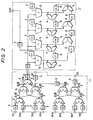
- Fig. 2 shows an example of the prior art of a video signal processor which functions as the aforementioned motion detection circuit.
- a signal processing block 1' located at the lefthand side of Fig. 2 and enclosed by broken lines detects the motion. First, signals delayed several pixels, several scanning lines and several fields are fed to registers 3 from terminals IN1 to IN8. Then averaging (interpolation) and subtraction are performed by arithmetic logic units 4. Basically the motion is detected by calculating the difference between successive frames.
- This signal processing block 1' is fed to a transversal filter, which is exemplified by a signal processing block 2' located at the righthand side of Fig. 2 and enclosed by broken lines.
- This filter is used to remove the high-frequency components of the motion signal. Motion signal cannot be used unless it is filtered through the transversal filter 2', which plays an important role.
- the circuit of the prior art shown in Fig. 2 is constructed of a number of ALUs, multipliers 5, registers 3, coefficient memories 7, delay memories 6 and so on.
- the transversal filter 2' uses a large number of components, especially in multipliers 5 and ALUs 4 about 3,000 transistors and about 1,000 transistors respectively, so that the circuit scale is enlarged to raise a problem.
- One of counter-measures against this problem is a method where multiplications are performed with a look-up table using RAMs (i.e., Random Access Memories). Even with this method, however, the number of elements or transistors used per tap of the transversal filter is still as large as about 5,000 so that the filter 2' (having a symmetrical coefficient of eight taps) of Fig.
- the high definition digital TV receiver uses as many as ten filters of this kind, so that the scale-down of these filter circuits is an important subject.
- the gate length of a MOS transistor is scaled down so that the device characteristics, especially the gate delay time gets shorter. Consequently, the critical path delay of the signal processing circuits, including multipliers and ALUs is improved.
- the critical path delay of an 8 x 8 bit multiplier is about 50 ns with 3 ⁇ m M O S transistors. This can be shortened to about 12 ns by using 0.8 ⁇ m M O S transistors.
- the sampling time of a digital TV system for example, is constant at 70 ns. The single use of each signal processing circuits for one sampling time is seriously wasteful.
- a time multiplex of at least five times can be accomplished to reduce the number of arithmetic logic units to be used to one fifth.
- An object of the present invention is to provide a circuit of a digital video signal processor to be used in systems such as high definition digital TV, efficiently using the time multiplexing processes.
- Embodiment 1 of the present invention will be described in the following with reference to Figs. 1, 2, 3 and 4.
- the lefthand signal processing block 1' uses nine ALUS 4 whereas the righthand signal processing block 2' uses seven ALUs 4 and four multipliers 5.
- each SPC is constructed in conformity to the above-specified requirements.
- the SPC 1 can be constructed of two ALUs at the least, and the SPC 2 can be constructed of two ALUs and one multiplier at the least.
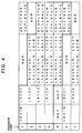
- SPC 1 and SPC 2 which are constructed by combining the above-specified numbers of the ALUs and the multiplier with registers, latches, delay memories and coefficient memories, are shown in Fig. 1. These SPC 1 and SPC 2 operate in accordance with the programs shown in Figs. 3 and 4, respectively.
- reference numeral 3 designates registers; numeral 4 ALUs; numeral 5 a multiplier; numeral 6 delay memories; numeral 7 a coefficient memory; numeral 8 latches; and numeral 9 data buses.
- input signals IN1 to IN8 are latched in registers R1 to R8.
- the arithmetic results (L1 + L2)/2 and (L3 + L4)/2 of the ALU4 are latched in the latches L1 and L3, and L2 and L4, respectively.
- the subsequent multiplied result is latched in the latches L8 and L10.
- a pipe-line process for executing the multiplication of the present data simultaneously with the addition of the preceding data is used.
- the two adders 4 operate in parallel.
- the program advances to the sixth step of Fig. 4 so that the process is similar to that of the circuit of Fig. 2.
- the succession and succeeding steps can be added to the first and sixth steps so that the sampling interval (e.g., five steps in Fig. 4) can be shortened.
- Instruction NOP appearing in Fig. 4 designate "No Operation", in which no operation is executed and which is inserted for the synchronization (i.e., five steps / sampling time) with the SPC 1.
- the program advances like the SPC 1 in response to the internal clock of 14 ns.
- the NOP can be eliminated to reduce the step number up to a rate of four steps / sampling time.
- the internal clock is generated by the PLL in each SPC, synchronized with the common sampling clock in the video system. Therefore, the internal clock may be common or independent for the individual SPCs.
- the description thus far made is a general one of the video signal processor using the SPCs according to the present invention.
- the SPC 1 and SPC 2 have the following features because of the motion detections executed in the SPCs and the circuit structure intrinsic to the transversal filter.
- the linear phase transversal filter uses the two adders 4 to operate in parallel. This takes it into consideration that after the inputs are multiplied with appropriate filter coefficients by the multiplier 5 its result are used in two additions simultaneously, as shown in Fig. 1. As in this case, the signal processing parallelism can be enhanced to increase the signal processing rate by making an SPC architecture according to the signal processing content.
- the SPC 1 of Fig. 1 also adopts the architecture considering the signal processing content.
- the four bus lines 9 are provided to enhance the parallelism of the data flow.
- Fig. 5 shows the circuit structure of the program memory 10.
- reference numeral 11 designate an address decoder; numeral 12 buffers; numeral 13 "1" level memory cells; numeral 14 "0" level memory cells; numeral 15 word lines; and numeral 16 data lines.
- reference letters L5E to L10E designate enable signals to be fed to the latches L5 to L10 of Fig.
- each of the memory cells 13 and 14 has the data line 16 connected directly with a power source V dd or grounded to the earth in accordance with its stored content.
- a power source V dd or grounded to the earth in accordance with its stored content.
- there are other options for these such as static RAMs, fusible PROMs, electrically writable EPROMs or electrically erasable EEPROMs.
- a circuit for generating the addresses of the afore-mentioned program memories is shown in Fig. 6, and its pulse timings are shown in Fig. 7.
- the internal clocks are generated by a PLL circuit (i.e., Phase Locked Loop).
- a voltage controlled oscillator 19 generates two-phase clocks ⁇ 1 and ⁇ 2, which are counted down by a binary counter 20 which is reset for every 5 counts in accordance with the fifth program step.
- 3-bit program memory addresses (a0, a1 and a2) are generated.
- a phase comparator 17 An accurate synchronization is taken by comparing the phases of the counted-down result a2 and the sampling clock CLKS of the input signal by means of a phase comparator 17.
- the aforementioned counter 20 is equipped with a reset terminal or a present terminal and a data input terminal.
- reference numeral 18 designates a low-pass filter.
- the circuit under consideration is provided either independently in each SPC or commonly for a plurality of SPCs. In either case, the value of the n-notated counter in the PLL circuit can be independently set so that the optimum instruction execution time for each SPC can be set.
- the clocks ⁇ 1 and ⁇ 2 can be fed from the outside if no problem arises in the speed.
- Fig. 8 shows the structure of the SPC 2 of Fig. 1 in case the interface with the SPC buses is taken into consideration.
- the device address (DA) from the external SPC bus 26 is decoded by a device decoder 23 of the SPC. If the derive address coincide with the address designated to that SPC, DS (Device Select) signal is issued.
- the program counter is switched by a multiplexer 24 from a main program counter 21 to a sub program counter 22 which is controlled by an external clock and a preset signal.
- the program for setting the coefficient of the program memory 10, the operation mode or the testing program is controlled by this sub program counter.
- the data (DT) from the SPC bus 26 are fed through an internal bus 25 to the coefficient memory 7.
- the system VLSI is arranged with a number of SPCs 28 (i.e., SPC 1 to SPC 5), as shown in Fig. 9. All of these SPCs are controlled either from the outside via the SPC bus 26 through an interface circuit 29 or by an internal processor 30.
- numeral 32 designates an external processor
- numeral 33 designates an external bus.
- the signals are processed along a high-speed signal path 31 indicated by hatched arrow.
- the interface circuit 29 or the internal processor 30 accesses a specific SPC to carry out those operations.
- the SPC performs the filtering operation at a high speed
- the internal processor performs complicated adaptation calculations. The coefficients thus calculated are transmitted during a blanking period in the TV scanning to the SPC filter via the aforementioned SPC bus.
- the transversal filter in the Embodiment 1 is enhanced, so that setting of the time multiplex degree becomes capable, and filters can be connected in cascade to have variable orders.
- this embodiment is equipped with a circuit for setting the number of frequency divisions of a counter in the phase locked loop circuit (PLL) an input signal delay circuit, a circuit to fed external data directly to an ALU, and a circuit for outputting the data to the outside directly from the ALU.
- PLL phase locked loop circuit
- the transversal filter of the Embodiment 1 of Fig. 1 is constructed of one SPC 2(2).
- the transversal filter of the present embodiment is constructed of two SPCs, i.e., SPC 2A(2A) and SPC 2B(2B) which are connected in cascade.
- a multiplex number N sets the number of frequency divisions of a frequency dividing counter 38 by a multiplex number register 37 and partially changes the content of the program memory 10. Since, moreover, the signal from the preceding stage can be transferred to the register L7 of the ALU 4 by an input switching circuit 35, the SPCs can be connected in cascade. This enables the filter to extend its order to an arbitrary value.
- Fig. 10 shows the SPC as includes not only the portion indicated at SPC 2 in Fig. 1 but also the program memory shown in Fig. 5 and the PLL portion shown in Fig. 6.
- the setting of the time multiplex number can be changed by setting the number of frequency divisions of the frequency dividing counter 38 in a PLL circuit 36 by means of a circuit shown in Fig. 11.
- the timing charts are shown in Fig. 12.
- a T flip-flop 39 alter the output Q in response to the fall of the input signal T.
- the output Q is reset by inputting a '0' signal to the reset terminal R.
- An exclusive OR circuit outputs the logical level 0, when each binary output Q1 of the T flip-flop and a time multiplex number N i coincide, and resets each T flip-flop 39 through an OR gate 40 at its output terminal only when all the bits coincide. This behavior is shown in Fig. 12.
- the reset signal RST there appear pulses from the voltage controlled oscillator VCO, which are compared for synchronization with the external CL.
- the present signal processor can be used six times time-multiplexly by using the output of the VCO as the control clocks. As a result, the number of frequency divisions of the counter and the time multiplex degree can be changed by setting the value of the time multiplex degree N.
- the circuit shown in Fig. 10 can be operated like the filter shown in Fig. 14 if it follows the programs shown in Figs. 13A and 13B.
- Two directions of signal flow are present in Fig. 14.
- One is a rightward signal flow of L7 - Z1 - Z3 - R13 and the other is a leftward signal flow of L10 - Z4 - Z2 - Z13.
- This is because the individual filter coefficients of the signals to be sequentially added are set at C1, C2, C3, - - -, and C3, C2, C1 by folding back the rightward signals leftward after they have passed through a predetermined number of steps of filters.
- This embodiment is modified from the transversal filter of the Embodiment 4 such that not only the tap coefficients but also the delay between each filter tap can be set.
- This filter circuit is appropriate for a ghost canceller circuit of a TV receiver or the like.
- Fig. 15 shows the structure of the SPC of the filter portion of the present embodiment.
- Each variable delay circuit 41 is constructed of: a shift register 42 for operating in synchronism with a sampling clock; a multiplexer 43 for selecting the outputs of the shift register; and a delay number register 44 for latching the delay number.
- the amount of delay of each delay circuit is set like the filter tap coefficient through a data bus 45.
- the filter tap coefficient is latched in the coefficient memory 7.
- letter 8 designates registers; numeral 46 an internal data bus; numeral 47 a delay circuit output multiplexer; numeral 48 an extension circuit input multiplexer; and numeral 49 an interface circuit (I/O).
- the coefficient memory 7 latches the filter tap coefficients for five taps.
- the present embodiment is featured by the fact that the variable delay circuits 41 are used as registers for latching delay data.
- a filter circuit shown in Fig. 16 can be realized with a small number of elements.
- the filter circuit of Fig. 16 is a ghost canceller for eliminating the ghost from by substracting the ghost signal synthesized by the filter from a ghost containing signal coming from the input terminal.
- the number of elements in the digital signal processor is reduced by the process of present invention so that an analog/digital (A/D) converter, a digital/analog (i.e., D/A) converter and so on can be integrated on a common single chip.
- A/D analog/digital
- D/A digital/analog
- Fig. 17 shows a circuit example of the digital signal processor of the prior art not using the process of the present invention, as has been reported on pp. 152 and 153, ISSCC “Digest of Technical Papers", 1986.
- This circuit separates an illuminance signal Y and a chrominance signal C from the NTSC composite video signal of a television system. The operations of this circuit will be described briefly in the following.
- An analog NTSC signal is converted into a 8-bit digital signal by an A/D converter 102 and is inputted to a digital signal processor 101.
- This digital signal is delayed a predetermined amount by line memories 108 and a delay memory 109 until it is fed as signals S1 to S9 to a signal difference estimator 115 or a differential estimator 116.
- Reference numerals 110, 111 and 113 designate an ALU, an absolute value circuit, and a coefficient circuit, respectively.
- the outputs of these signal difference estimator 115 and differential estimator 116 becomes the control signal for the adaptive Y/C separation and fed to multiplexers 112.
- the NTSC composite signal is separated adaptively into 8-bit digital illuminance and chrominance signals, and are outputted from the digital signal processor 101 so that they are converted into analog illuminance and chrominance signals Y and C.
- this digital signal processor is designed by the technology based on the present invention, the number of circuit elements of the digital signal processor can be drastically reduced so that the A/D converter and the D/A converter can be integrated on the chip shared with the digital signal processor by making use of the reduced space on the chip, as shown in Fig. 18.
- reference numerals 104-1, 104-2 and 104-3 designate the individual portions of the digital signal processor, in which the number of elements is reduced by the process of the present invention.
- Numerals 117 and 118 designate a register and a bus line, respectively.
- the A/D converter 102 and the D/A converter 103 are integrated on the chip shared with the digital signal processor by making use of the space which is established by reducing the element number.
- the number of signal input spin is only one for the analog NTSC and only two for the analog Y and C, so that the number of pins, and consequently the price of the package can be reduced drastically.
Landscapes
- Engineering & Computer Science (AREA)
- Multimedia (AREA)
- Signal Processing (AREA)
- Filters That Use Time-Delay Elements (AREA)
- Television Systems (AREA)
Claims (3)
- Circuit de traitement de signaux vidéo numériques comportant
un premier bloc de traitement de signaux (1) pour effectuer une opération arithmétique sur les signaux vidéo originaux qui lui sont appliqués, et
un second bloc de traitement de signaux (2) pour effectuer une opération arithmétique sur les signaux vidéo délivrés par le premier bloc de traitement de signaux (1), le second bloc de traitement comprenant une borne d'entrée (IN) pour recevoir des échantillons de signal vidéo de longueur de données prédéterminée, une multiplicateur (5) relié à la borne d'entrée (IN), une unité logique arithmétique (4) reliée au multiplicateur (5), et une borne de sortie (OUT) reliée à l'unité arithmétique (4), caractérisé en ce que
le multiplicateur (5) multiplie chaque échantillon de signal vidéo de longueur de données prédéterminée reçu sur la borne d'entrée (IN) avec l'un d'une pluralité de premiers coefficients (C1 ∼ C4),
en ce que l'unité logique arithmétique (4) effectue une opération arithmétique sur chaque signal de sortie du multiplicateur (5) et l'un d'une pluralité de seconds coefficients (Z1 ∼ Z3),
en ce qu'un circuit bascule (6) est disposé pour verrouiller consécutivement chacun des signaux de sortie de l'unité logique arithmétique (4) et l'appliquer à l'unité logique arithmétique (4) en tant que l'un desdits seconds coefficients (Z1 ∼ Z3), et
en ce que le multiplicateur (5) et l'unité logique arithmétique (4) effectuent une pluralité d'opérations à l'intérieur d'une période de temps entre l'arrivée d'un échantillon de signal vidéo de longueur de données prédéterminée sur la borne d'entrée (IN) et le suivant. - Circuit selon la revendication 1, dans lequel le second bloc de traitement de signaux (2) comprend en outre
une pluralité de circuits de retard (8) disposés entre la borne d'entrée (IN) et le multiplicateur (5) et entre le multiplicateur et l'unité logique arithmétique (4),
un registre de mémoire (7) pour mémoriser lesdits premiers coefficients (C1 ∼ C4), et
un circuit de retard de sortie (3) disposé entre l'unité logique arithmétique (4) et la borne de sortie (OUT). - Circuit selon la revendication 1, dans lequel le premier bloc de traitement de signaux (1) comprend une pluralité de bornes d'entrée (IN1 ∼ IN8) et effectue une opération arithmétique sur les signaux vidéo originaux appliqué à ladite pluralité de bornes d'entrée (IN1 ∼ IN8).
Applications Claiming Priority (6)
| Application Number | Priority Date | Filing Date | Title |
|---|---|---|---|
| JP142998/86 | 1986-06-20 | ||
| JP61142998A JPH0828834B2 (ja) | 1986-06-20 | 1986-06-20 | 信号処理装置 |
| JP161843/86 | 1986-07-11 | ||
| JP16184386A JPS6318812A (ja) | 1986-07-11 | 1986-07-11 | 半導体集積回路装置 |
| JP190519/86 | 1986-08-15 | ||
| JP61190519A JPS6348079A (ja) | 1986-08-15 | 1986-08-15 | 半導体集積回路装置 |
Publications (3)
| Publication Number | Publication Date |
|---|---|
| EP0249962A2 EP0249962A2 (fr) | 1987-12-23 |
| EP0249962A3 EP0249962A3 (en) | 1990-03-21 |
| EP0249962B1 true EP0249962B1 (fr) | 1994-05-04 |
Family
ID=27318550
Family Applications (1)
| Application Number | Title | Priority Date | Filing Date |
|---|---|---|---|
| EP87108699A Expired - Lifetime EP0249962B1 (fr) | 1986-06-20 | 1987-06-16 | Processeur de signal vidéo numérique |
Country Status (3)
| Country | Link |
|---|---|
| US (1) | US4825287A (fr) |
| EP (1) | EP0249962B1 (fr) |
| DE (1) | DE3789731T2 (fr) |
Families Citing this family (22)
| Publication number | Priority date | Publication date | Assignee | Title |
|---|---|---|---|---|
| US5379351A (en) * | 1992-02-19 | 1995-01-03 | Integrated Information Technology, Inc. | Video compression/decompression processing and processors |
| FR2652973B1 (fr) * | 1989-10-06 | 1993-12-24 | Laboratoire Europ Recherc Electr | Interpolateur pour televiseur et televiseur comportant un tel interpolateur. |
| GB2240684B (en) * | 1990-02-06 | 1994-02-23 | Sony Corp | Digital signal interpolation |
| US5285264A (en) * | 1990-03-30 | 1994-02-08 | Kabushiki Kaisha Toshiba | Image reproduction apparatus with plural program processing |
| JPH03283976A (ja) * | 1990-03-30 | 1991-12-13 | Toshiba Corp | 画像再生装置 |
| US6324120B2 (en) | 1990-04-18 | 2001-11-27 | Rambus Inc. | Memory device having a variable data output length |
| IL96808A (en) | 1990-04-18 | 1996-03-31 | Rambus Inc | Introductory / Origin Circuit Agreed Using High-Performance Brokerage |
| US6751696B2 (en) * | 1990-04-18 | 2004-06-15 | Rambus Inc. | Memory device having a programmable register |
| US5594813A (en) * | 1992-02-19 | 1997-01-14 | Integrated Information Technology, Inc. | Programmable architecture and methods for motion estimation |
| US6965644B2 (en) * | 1992-02-19 | 2005-11-15 | 8×8, Inc. | Programmable architecture and methods for motion estimation |
| WO1994020927A1 (fr) * | 1993-03-12 | 1994-09-15 | Integrated Information Technology, Inc. | Architecture programmable et methodes d'estimation de mouvements |
| KR0140964B1 (ko) * | 1994-10-28 | 1998-06-15 | 구자홍 | 텔레비젼(tv) 수상기의 통신 제어 장치와 통신 제어방법 |
| US5623311A (en) * | 1994-10-28 | 1997-04-22 | Matsushita Electric Corporation Of America | MPEG video decoder having a high bandwidth memory |
| EP0710033A3 (fr) * | 1994-10-28 | 1999-06-09 | Matsushita Electric Industrial Co., Ltd. | Décodeur vidéo MPEG avec une mémoire à large bande |
| US5920352A (en) * | 1994-10-28 | 1999-07-06 | Matsushita Electric Industrial Co., Ltd. | Image memory storage system and method for a block oriented image processing system |
| US6085309A (en) * | 1997-01-08 | 2000-07-04 | Yamaha Corporation | Signal processing apparatus |
| EP1122637A3 (fr) * | 2000-01-31 | 2005-10-12 | Micronas GmbH | Unité de calcul pour le traitement de signaux limité |
| DE10009451C1 (de) * | 2000-01-31 | 2001-05-03 | Micronas Gmbh | Recheneinheit für eingeschränkte Signalverarbeitung |
| KR100377176B1 (ko) * | 2000-06-12 | 2003-03-26 | 주식회사 하이닉스반도체 | 데이터 암호화 표준 알고리즘을 이용한 암호화 장치 |
| US8526486B2 (en) * | 2008-11-12 | 2013-09-03 | Intel Corporation | Decision feedback equalizer for portable environments |
| US8504961B2 (en) * | 2010-06-01 | 2013-08-06 | Arm Limited | Integrated circuit with timing adjustment mechanism |
| CN110596889A (zh) | 2018-06-13 | 2019-12-20 | 托比股份公司 | 眼睛跟踪装置和制造眼睛跟踪装置的方法 |
-
1987
- 1987-06-16 EP EP87108699A patent/EP0249962B1/fr not_active Expired - Lifetime
- 1987-06-16 DE DE3789731T patent/DE3789731T2/de not_active Expired - Fee Related
- 1987-06-18 US US07/063,476 patent/US4825287A/en not_active Expired - Fee Related
Non-Patent Citations (1)
| Title |
|---|
| Computer Architectures and Parallel Processing, Hwang and Briggs, International Edition, 1985, McGraw-Hill Book Co., Singapore, pages 145 to 151 * |
Also Published As
| Publication number | Publication date |
|---|---|
| EP0249962A2 (fr) | 1987-12-23 |
| US4825287A (en) | 1989-04-25 |
| DE3789731D1 (de) | 1994-06-09 |
| EP0249962A3 (en) | 1990-03-21 |
| DE3789731T2 (de) | 1994-08-18 |
Similar Documents
| Publication | Publication Date | Title |
|---|---|---|
| EP0249962B1 (fr) | Processeur de signal vidéo numérique | |
| US5327125A (en) | Apparatus for and method of converting a sampling frequency according to a data driven type processing | |
| EP0287333B1 (fr) | Dispositif de "zoom" pour image de télévision | |
| EP0287331B1 (fr) | Système à mémoire de données échantillonnées, par exemple pour un système d'agrandissement d'une image de télévision | |
| US4644488A (en) | Pipeline active filter utilizing a booth type multiplier | |
| US5793443A (en) | Motion vector detection circuit | |
| EP0100678B1 (fr) | Système de séparation des signaux de circulation de données réduites | |
| EP0450260B1 (fr) | Circuit de filtrage pour signaux numériques | |
| US5034907A (en) | Dynamically configurable signal processor and processor arrangement | |
| KR970007011B1 (ko) | 직렬 비디오 프로세서와 고장 허용성 직렬 비디오 프로세서 장치 및 프로세스 방법 | |
| US4694413A (en) | Compact-structure input-weighted multitap digital filters | |
| EP0435951B1 (fr) | Traitement de signaux video et memoires video | |
| US5935197A (en) | Data processing circuit and method of operation performing arithmetic processing on data signals | |
| US5668895A (en) | Digital filter for image processing | |
| US5838387A (en) | Digital video scaling engine | |
| KR960004127B1 (ko) | 입력가중형 트랜스버셜 필터 | |
| US5349547A (en) | Bidimensional FIR filter | |
| Joanblanq et al. | A 54-MHz CMOS programmable video signal processor for HDTV applications | |
| KR940001556B1 (ko) | 디지탈신호처리장치 | |
| Yamazaki et al. | A 1-GOPS CMOS programmable video signal processor | |
| US7623721B1 (en) | High-speed dithering architecture | |
| JPH0240688A (ja) | 実時間動画処理方式及び装置 | |
| JPS60129890A (ja) | デイジタル信号処理装置 | |
| US6072911A (en) | Linear image filter and the corresponding filtering method | |
| JP3352558B2 (ja) | 信号処理装置 |
Legal Events
| Date | Code | Title | Description |
|---|---|---|---|
| PUAI | Public reference made under article 153(3) epc to a published international application that has entered the european phase |
Free format text: ORIGINAL CODE: 0009012 |
|
| AK | Designated contracting states |
Kind code of ref document: A2 Designated state(s): DE FR GB |
|
| PUAL | Search report despatched |
Free format text: ORIGINAL CODE: 0009013 |
|
| AK | Designated contracting states |
Kind code of ref document: A3 Designated state(s): DE FR GB |
|
| 17P | Request for examination filed |
Effective date: 19900829 |
|
| 17Q | First examination report despatched |
Effective date: 19920626 |
|
| GRAA | (expected) grant |
Free format text: ORIGINAL CODE: 0009210 |
|
| AK | Designated contracting states |
Kind code of ref document: B1 Designated state(s): DE FR GB |
|
| REF | Corresponds to: |
Ref document number: 3789731 Country of ref document: DE Date of ref document: 19940609 |
|
| ET | Fr: translation filed | ||
| PLBE | No opposition filed within time limit |
Free format text: ORIGINAL CODE: 0009261 |
|
| STAA | Information on the status of an ep patent application or granted ep patent |
Free format text: STATUS: NO OPPOSITION FILED WITHIN TIME LIMIT |
|
| 26N | No opposition filed | ||
| PGFP | Annual fee paid to national office [announced via postgrant information from national office to epo] |
Ref country code: DE Payment date: 19950828 Year of fee payment: 9 |
|
| PG25 | Lapsed in a contracting state [announced via postgrant information from national office to epo] |
Ref country code: DE Effective date: 19970301 |
|
| PGFP | Annual fee paid to national office [announced via postgrant information from national office to epo] |
Ref country code: GB Payment date: 19980605 Year of fee payment: 12 |
|
| PGFP | Annual fee paid to national office [announced via postgrant information from national office to epo] |
Ref country code: FR Payment date: 19980616 Year of fee payment: 12 |
|
| PG25 | Lapsed in a contracting state [announced via postgrant information from national office to epo] |
Ref country code: GB Free format text: LAPSE BECAUSE OF NON-PAYMENT OF DUE FEES Effective date: 19990616 |
|
| PG25 | Lapsed in a contracting state [announced via postgrant information from national office to epo] |
Ref country code: FR Free format text: THE PATENT HAS BEEN ANNULLED BY A DECISION OF A NATIONAL AUTHORITY Effective date: 19990630 |
|
| GBPC | Gb: european patent ceased through non-payment of renewal fee |
Effective date: 19990616 |
|
| REG | Reference to a national code |
Ref country code: FR Ref legal event code: ST |