EP0244907B1 - Geschalteter Spannungswandler - Google Patents
Geschalteter Spannungswandler Download PDFInfo
- Publication number
- EP0244907B1 EP0244907B1 EP87200803A EP87200803A EP0244907B1 EP 0244907 B1 EP0244907 B1 EP 0244907B1 EP 87200803 A EP87200803 A EP 87200803A EP 87200803 A EP87200803 A EP 87200803A EP 0244907 B1 EP0244907 B1 EP 0244907B1
- Authority
- EP
- European Patent Office
- Prior art keywords
- connection
- voltage
- coil
- capacitor
- switching element
- Prior art date
- Legal status (The legal status is an assumption and is not a legal conclusion. Google has not performed a legal analysis and makes no representation as to the accuracy of the status listed.)
- Expired - Lifetime
Links
Images


Classifications
-
- H—ELECTRICITY
- H02—GENERATION; CONVERSION OR DISTRIBUTION OF ELECTRIC POWER
- H02M—APPARATUS FOR CONVERSION BETWEEN AC AND AC, BETWEEN AC AND DC, OR BETWEEN DC AND DC, AND FOR USE WITH MAINS OR SIMILAR POWER SUPPLY SYSTEMS; CONVERSION OF DC OR AC INPUT POWER INTO SURGE OUTPUT POWER; CONTROL OR REGULATION THEREOF
- H02M1/00—Details of apparatus for conversion
- H02M1/32—Means for protecting converters other than automatic disconnection
- H02M1/34—Snubber circuits
-
- H—ELECTRICITY
- H02—GENERATION; CONVERSION OR DISTRIBUTION OF ELECTRIC POWER
- H02M—APPARATUS FOR CONVERSION BETWEEN AC AND AC, BETWEEN AC AND DC, OR BETWEEN DC AND DC, AND FOR USE WITH MAINS OR SIMILAR POWER SUPPLY SYSTEMS; CONVERSION OF DC OR AC INPUT POWER INTO SURGE OUTPUT POWER; CONTROL OR REGULATION THEREOF
- H02M3/00—Conversion of dc power input into dc power output
- H02M3/02—Conversion of dc power input into dc power output without intermediate conversion into ac
- H02M3/04—Conversion of dc power input into dc power output without intermediate conversion into ac by static converters
- H02M3/10—Conversion of dc power input into dc power output without intermediate conversion into ac by static converters using discharge tubes with control electrode or semiconductor devices with control electrode
- H02M3/145—Conversion of dc power input into dc power output without intermediate conversion into ac by static converters using discharge tubes with control electrode or semiconductor devices with control electrode using devices of a triode or transistor type requiring continuous application of a control signal
- H02M3/155—Conversion of dc power input into dc power output without intermediate conversion into ac by static converters using discharge tubes with control electrode or semiconductor devices with control electrode using devices of a triode or transistor type requiring continuous application of a control signal using semiconductor devices only
- H02M3/156—Conversion of dc power input into dc power output without intermediate conversion into ac by static converters using discharge tubes with control electrode or semiconductor devices with control electrode using devices of a triode or transistor type requiring continuous application of a control signal using semiconductor devices only with automatic control of output voltage or current, e.g. switching regulators
- H02M3/158—Conversion of dc power input into dc power output without intermediate conversion into ac by static converters using discharge tubes with control electrode or semiconductor devices with control electrode using devices of a triode or transistor type requiring continuous application of a control signal using semiconductor devices only with automatic control of output voltage or current, e.g. switching regulators including plural semiconductor devices as final control devices for a single load
-
- H—ELECTRICITY
- H02—GENERATION; CONVERSION OR DISTRIBUTION OF ELECTRIC POWER
- H02M—APPARATUS FOR CONVERSION BETWEEN AC AND AC, BETWEEN AC AND DC, OR BETWEEN DC AND DC, AND FOR USE WITH MAINS OR SIMILAR POWER SUPPLY SYSTEMS; CONVERSION OF DC OR AC INPUT POWER INTO SURGE OUTPUT POWER; CONTROL OR REGULATION THEREOF
- H02M1/00—Details of apparatus for conversion
- H02M1/32—Means for protecting converters other than automatic disconnection
- H02M1/34—Snubber circuits
- H02M1/346—Passive non-dissipative snubbers
-
- Y—GENERAL TAGGING OF NEW TECHNOLOGICAL DEVELOPMENTS; GENERAL TAGGING OF CROSS-SECTIONAL TECHNOLOGIES SPANNING OVER SEVERAL SECTIONS OF THE IPC; TECHNICAL SUBJECTS COVERED BY FORMER USPC CROSS-REFERENCE ART COLLECTIONS [XRACs] AND DIGESTS
- Y02—TECHNOLOGIES OR APPLICATIONS FOR MITIGATION OR ADAPTATION AGAINST CLIMATE CHANGE
- Y02B—CLIMATE CHANGE MITIGATION TECHNOLOGIES RELATED TO BUILDINGS, e.g. HOUSING, HOUSE APPLIANCES OR RELATED END-USER APPLICATIONS
- Y02B70/00—Technologies for an efficient end-user side electric power management and consumption
- Y02B70/10—Technologies improving the efficiency by using switched-mode power supplies [SMPS], i.e. efficient power electronics conversion e.g. power factor correction or reduction of losses in power supplies or efficient standby modes
Definitions
- the invention relates to a switched voltage converter having at least one controlled semiconductor switch and a first coil each having a first and a second connection, the first connections being connected together in a series arrangement with at least the one controlled semiconductor switch and the first coil present between supply voltage terminals, said controlled semiconductor switch being connected to a terminal for the supply of a switching signal for turning the semiconductor switch alternately on and off for obtaining a desired voltage at a converter terminal, the first coil being coupled to a first connection of an inductive load formed with the first and a second connection and the second connection of the first coil being coupled to a first electrode of a first semiconductor switching element formed with the first and a second electrode, the first connections of the semiconductor switch and the first coil being connected to a first terminal of a capacitor, a second terminal of which is connected via a series arrangement with a second semiconductor switching element and a second coil to the second connection of the semiconductor switch, the second terminal of the capacitor being connected to a first electrode of a third semiconductor switching element formed with the first and a second electrode, the current pass direction of the controlled
- a voltage converter of this type is described in European Patent Application EP-A- 82 071.
- the converter has no resistors.
- the dissipation is mainly present upon turning on and off the controlled semiconductor switch in the form of a bipolar transistor and the semiconductor switching elements in the form of diodes.
- two speed limiting circuits for voltage changes and current changes, respectively, are provided which are commonly referred to as "snubber" circuits.
- these circuits are formed by connecting the second electrode of the third semiconductor switching element formed as a diode to a supply voltage terminal conveying a voltage halfway the supply voltage occurring across the said series arrangement of the transistor, the first coil and the first diode.
- the capacitor thereby prevents a too rapid increase of the switching voltage upon turning off the transistor, which increase is caused by the energy stored in the first coil, whilst the third diode is conducting.
- the transistor is turned on, a too high switching current through this transistor caused by discharging of the capacitor is prevented by the second coil which is present in series with the then conducting second diode.
- a switched voltage converter according to the invention is characterized in that the second electrode of the third semiconductor switching element is coupled via a second capacitor to the second connection of the first coil and is coupled via a fourth semiconductor switching element in a d.c. connection comprising the third and fourth semiconductor switching elements to the second electrode of the first semiconductor switching element in respect of which electrode the first and fourth semiconductor switching elements have the same current pass direction.
- the capacitance of the first-mentioned and the second capacitor can be chosen as desired for obtaining a limited switching overvoltage upon turning off the controlled semiconductor switch.
- the capacitance of the second capacitor also determines the maximum voltage across the first and fourth semiconductor switching elements.
- the fourth semiconductor switching element is active as a clamping diode in the same manner as the first semiconductor switching element.
- an embodiment of a voltage converter according to the invention is characterized in that the second electrode of the third semiconductor switching element is connected both via a third capacitor to the second connection of the semiconductor switch and via a fifth semiconductor switching element to a junction point between the second capacitor and the fourth semiconductor switching element, the third, fifth and fourth semiconductor switching elements having the same current pass direction constituting the said d.c. connection.
- An embodiment in which a choice can be made which converter terminal is active as an output terminal of the converter at the desired voltage is characterized in that in the case of a connection of a first supply voltage terminal to the second connection of the semiconductor switch and of a second supply voltage terminal to the second electrode of the first semiconductor switching element or to the second connection of the inductive load, the said converter terminal conveying the desired voltage is connected to the second connection of the inductive load or to the second electrode of the first semiconductor switching element, respectively.
- a switched voltage converter in the form of a symmetrical converter having two controlled semiconductor switches one of which is connected to the one connection and the other of which is connected to the other connection of the first coil, in which the first connection of the inductive load is connected to a tapping on the first coil and each controlled semiconductor switch is present in an associated circuit formed with the first-mentioned and second capacitors, the second coil and the first, second, third and fourth semiconductor switching elements, is characterized in that in the associated circuit the second electrode of each third semiconductor switching element is connected via a third capacitor to the second connection of the relevant semiconductor switch.
- a further embodiment is characterized in that the first coil and the second coil are wound on a common core.
- the first coil and the second coil are wound on a common core.
- An embodiment of a voltage converter according to the invention with a high-frequency decoupling between supply voltage terminals and a converter output terminal is characterized in that the second connection of the inductive load is connected via a fourth and a fifth capacitor to the second connection of the semiconductor switch and to the second electrode of the first semiconductor switching element, respectively.
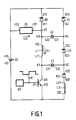
- Fig. 1 shows a circuit diagram of a switched voltage converter according to the invention which operates with a snubber circuit for current changes only
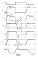
- Fig. 2 shows some signal diagrams as a function of time to illustrate the operation of the converter of Fig. 1,
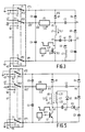
- Figs 3 and 5 show circuit daigrams of a converter operating with snubber circuits for both current and voltage changes
- Figs. 4 and 6 show associated signal diagrams
- Fig. 7 shows a first circuit diagram of a symmetrical converter according to the invention, operating with snubber circuits for both current and voltage changes,
- Fig. 8 shows associated signal diagrams
- Fig. 9 shows a second circuit diagram of a symmetrical converter embodiment.
- the signal diagram G1T is associated with a switching signal which has a square-wave variation in a cycle between two values which are not indicated.
- Fig. 4 shows an entire duty cycle at the converter according to Fig. 3.
- the signal diagrams V1 to V5 are voltage diagrams in which possibly present supply voltage values are denoted by +VS, -VS and 0V as the ground potential.
- the signal diagram IL1 shows a current diagram in which a current value IL0 and a zero current 0A are denoted.
- Fig. 1 shows a controlled semiconductor switch S1, a first coil L1 connected thereto and a subsequent semiconductor switching element D1 which are present between supply voltage terminals -VS and +VS of a supply voltage source VS.
- the semiconductor switch S1 is shown as a bipolar transistor of the npn type.
- the collector of the transistor S1 is indicated by a first connection S11 and its emitter is indicated by a second connection S12 which is connected to the terminal -VS.
- the base of the transistor S1 is connected to a terminal G1T for the supply of a switching signal denoted by the same reference, which signal originates from a switching signal generator G1.
- the transistor S1 functioning as a controlled semiconductor switch is alternately conducting and non-conducting, or in other words turned on and turned off.
- the switch S1 may be in the form of a field effect transistor, a thyristor or a controlled semiconductor switch of another type.
- the first connection S11 of the switch S1 is connected to a first connection L11 of the first coil L1 at which a second connection L12 is shown.
- the coil L1 may be formed with or without a core which is shown by a broken line.
- an arrow denotes the positive current direction of a current IL1 possibly flowing through the coil.
- V1 the voltage occurring thereacross is denoted by V1.
- the second connection L12 of the coil L1 is coupled to a first electrode D11 of the semiconductor switching element D1 shown as a diode, which element has also a second electrode D12 connected to the supply voltage terminal +VS.
- the first and second electrodes D11 and D12 are the anode and the cathode, respectively, of the diode D1.
- Fig. 1 shows a second, third and fourth semiconductor switching element D2, D3 and D4 formed as diodes with first and second electrodes D21 and D22, D31 and D32 and D41 and D42, respectively. It will be evident from the description of the circuit diagrams of Figs. 7 and 9 that the semiconductor switching element D1 may form part of a controlled semiconductor switch in the form of a field effect transistor conducting current in two directions.
- a junction point conveying the voltage V5 is shown between the connection L12 and the electrode D11 and a converter terminal 0T conveying a desired voltage to be supplied to a first connection L01 of an inductive load L0, a second connection L02 of which is connected to the supply voltage terminal +VS.
- the inductive load L0 is, for example, a motor coil of a d.c. motor.
- the presence of an inductive/ohmic series arrangement or network is mentioned as a further example.
- the inductance of the inductive load L0 is so large that in the switching converter this load conveys a substantially constant current ILO whose positive current direction is denoted by an arrow.
- connections S11 and L11 conveying the voltage V1 are connected to a first terminal C11 of a first capacitor C1 which has also a second terminal C12 on which the voltage V2 occurs.
- the terminal C12 is connected to the connection S12 of the switch S1 via a series arrangement of the second diode D2 as a semiconductor switching element and a second coil L2.
- a first connection L21 of the second coil L2 formed, for example, with a core is connected to the anode as a first electrode D21 of the diode D2.
- the diode D2 and the coil L2 may change position.
- the second capacitor terminal C12 is also connected to an anode as a first electrode D31 of the third semiconductor switching element formed as a diode D3.
- the cathode as a second electrode D32 conveying the voltage V4 is connected both to a first terminal C21 of a second capacitor C2 and to an anode as a first electrode D41 of the fourth semiconductor switching element in the form of diode D4.
- the terminal C22 is connected to the connection L12 of the coil L1.
- the cathode as a second electrode D42 of the diode D4 is connected to the cathode D12 of the diode D1 so that both have the same current pass direction with respect to the junction point.
- Fig. 1 the current pass directions of the transistor S1 and the diodes D1, D2, D3 and D4 are shown in relation to the given polarity at the supply voltage terminals + VS and -VS.
- the current pass direction of the transistor S1 with respect to a given direction of the current through the first capacitor C1, is equal to that of the first diode D1 and the second diode D2 and is opposite to that of the third diode D3 and the fourth diode D4.
- the starting point is a first stable (initial) state in which the switch S1 is turned on. Subsequently the switch is turned off and after reaching another second stable state, the switch is turned on again whereafter the first stable state is reached again.
- the switching signal G1T shown in Fig. 2 is associated therewith. Before the instant t1,t2 and in the initial state the current IL0 flows from the terminal +VS to the terminal -VS via the inductive load L0, the coil L1 and the transistor S1.
- IL1 ILO
- the capacitors C1 and C2 both convey a voltage (VS-Va).
- the diodes D are non-conductive, whilst the diodes D1, D2 and D4 are in the , cut-off state and the diode D3 is biased into its conducting state due to the presence of the same voltage at anode and cathode. In the description of the operation of the diodes D, diode threshold voltages and diode voltage drops in the conductivity direction are ignored.
- the transistor S1 is turned off and voltage steps shown at the voltages V1, V2, V4 and V5 occur.
- the voltages V2 and V4 indicate that upon reaching the value +VS at this instant the diodes D3 and D4 start conducting and operate as clamping diodes.
- the current IL1 charges the capacitor C1 and the current (ILO-IL1) discharges the capacitor C2, which is evident from the voltages V1 and V5 and current IL1 shown.
- the voltages V2 and V4 then maintain the value +VS.
- the current IL1 further charges the capacitor C1 (increasing voltage V1) until this current becomes zero. During this period the voltages, V2, V4 and V5 maintain the value +VS.
- IL1 0A and the diode D3 is cut off.
- the voltage across the coil L1 becomes equal to zero (VL1 becomes 0V) and a voltage step VC1 occurs in the voltages V1 and V2.
- the voltage VC1 is the voltage across the charged capacitor C1.
- the second stable state is present in which the current IL0 flows in a circuit with the inductive load L0 and the diode D1.
- the non-conducting diode D4 is biased into its conducting state when the transistor S1 is turned off and the diodes D2 and D3 are cut off.
- the transistor S1 is turned on under the control of the switching signal G1T.
- the voltage V1 acquires a voltage step to the value -VS, whilst the same step gives the value (-VS -VC1) in the voltage V2 via the capacitor C1, whereupon the diode D2 can start conducting.
- the energy stored in the coil L2 produces a current through the coil L2 and the diode D2 which directly charges the capacitor C1 and charges the capacitor C2 through the diode D3 and the coil L1 until the current through the coil L2 becomes zero.
- the voltages V2 and V4 change to the value -Va.
- the voltage V5 has the variation shown.
- the increase of the current through the coil L1 is shown at the current IL1.
- the transistor S1 When the transistor S1 is turned on at the instant t5, the voltage thereacross immediately drops off so that the turn-on losses determined by the product of voltage thereacross and the current therethrough are at a minimum. Furthermore the current through the diode D1 gradually decreases in the period t5 to t6,t7 so that cutting off of the diode D1 at the instant t6,t7 is accompanied by minimum turn-off losses, whilst the overvoltage VC1 in the switching voltage V2 is obtained as desired by the choice of the capacitance for the capacitors C1 and C2.
- Fig. 1 If there must be snubber circuits for both current and voltage changes, this can be realised in Fig. 1 by detaching the second electrode D32 of the third diode D3 from the junction point conveying the voltage V4 and by connecting it thereto via a fifth diode D5 having the same current pass direction. Furthermore the eleetrode D32 is connected via a third capacitor C3 to the second connection S12 of the transistor S1. The junction point conveying the voltage V2 is now connected to the cathode of the diode D1 via the d.c. connection with the diodes D3, D5 and D4, whilst the junction point of the diodes D3 and D5 and the capacitor C3 conveys the voltage V3. In Figs. 3 and 5 these connections are shown at asymmetrical voltage converters which are also further modified.
- the voltage converters according to Figs. 3 and 5 are formed with an internal inductive load L0 whose second connection L02 can be connected to a converter output terminal -0T or a supply voltage terminal conveying the voltage +VS or the ground potential.
- the converter according to Figs. 3 and 5 is provided, for example, with a changeover device VT formed with connection terminals VT1, VT2 and VT2 ⁇ via which device converter output terminals +0T and -0T and supply voltage terminals conveying the voltages +VS and -VS and the ground potential at 0V can be connected, respectieely to the connection S12 of the transistor S1, the cathode D12 of the diode D1 or the connection L02 of the internal inductive load L0.
- the connection L02 of the load L0 is connected via respective fourth and fifth capacitors C4 and C5, to the connection S12 or the cathode D12.
- the change-over device VT is shown with three coupled change-over switches VS1, VS2 and VS3 each having three change-over terminals T1, T2 and T3.
- the terminals VT1 and VT2 are connected to the voltage -VS and to ground, respectively, and the terminal VT2 ⁇ is connected to the converter output terminal -0T.
- the terminals VT1 and VT2 ⁇ are connected to ground and to the voltage +VS, respectively.
- the terminals VT1 and VT2 ⁇ are connected to the voltage -VS and to ground, respectively.
- the converter output terminal +0T is connected to the terminal VT2.
- the converter according to Fig. 3 or 5 can be used in all three known basic forms of switched voltage converters.
- the converter in the state T1 operates as a series or forward converter, in the state T2 as a step-up converter and in the state T3 as a parallel or reverse converter.
- the converter output terminals -0T and +0T are available for connection to an ohmic, ohmic-inductive or ohmic-capacitive load not shown.
- the current ILO in the assumed first stable (initial) state flows from the terminal VT2 ⁇ to the terminal VT1 conveying the voltage -VS via the internal inductive load L0, the coil L1 and the transistor S1.
- IL1 IL0
- the capacitors C1, C2 and C3 each convey a voltage (VS-Vb).
- the diodes D1, D2 and D4 of the non-conducting diodes D are in the cut-off state and the diodes D3 and D5 are biased into their state of conductance.
- the transistor S1 is turned off under the control of the switching signal G1T.
- the decreasing current IL1 charges the capacitor C1 and, via the conducting diode D3, the capacitor C3.
- the converter of Fig. 3 operates with a snubber circuit (D3, C3) for voltage changes dV/dt.
- the current IL1 further charges the capacitor C1 (voltage V1) until this current in the resonant circuit (L1, C1) becomes zero. During this period the voltages V2, V3, V4 and V5 maintain the voltage 0V.
- IL1 0A and the diode D3 is cut off.
- the voltage across the coil L1 now becomes zero (VL1 becomes 0V) and a voltage step VC1 occurs in the voltages V1 and V2.
- the voltage VC1 is the voltage across the completely charged capacitor C1.
- the second stable state is present in which the current IL0 flows from the terminal VT2 ⁇ . via the load L0 and the diode D1 to the terminal VT2.
- the capacitor C1 conveys the voltage VC1 and the capacitor C3 conveys the voltage VS.
- the diodes D2 and D3 of the non-conducting diodes D2, D3, D4 and D5 are in the cut-off state and the diodes D4 and D5 are biased into their conducting state.
- the transistor S1 is turned on under the control of the switching signal G1T.
- the voltage V1 acquires a voltage step to the value -VS while the same step gives the value (-VS - VC1) via the charged capacitor C1 in the voltage V2. Consequently the diode D2 can start conducting.
- the capacitor C1 is further discharged in the resonant circuit (L2, C1).
- the increase of the current through the coil L1 is shown at the current IL1.
- V3 V2 at which the diode D3 starts conducting.
- IL1 IL0 at which the diode D5 is cut off and the voltage across the coil L1 has become zero.
- the result is a voltage step in the voltages V4 and V5 so that the voltage V4 acquires the value -Vb and the voltage V5 acquires the value -VS.
- the first stable (initial) state is present again until the instant t1 of the next duty cycle.
- the voltage (VS - Vb) is present across all three capacitors C1, C2 and C3.
- the converter of Fig. 5 differs from the converter shown in Fig. 3 in that the first coil L1 and the second coil L2 are wound on a common core. Apart from the advantage of saving a core if core-provided coils L1 and L2 are used, the converter of Fig. 5 has a lower voltage change rate upon turning off the transistor S1, lower switching overvoltages and shorter transient phenomena.
- the coil L1 is wound in a given direction on the core, starting from the connection L11 to the connection L12, whilst the coil L2 is wound in the same direction, starting from the connection L22 to the connection L21.
- Polarity dots are shown at the connections L11 and L21.
- Fig. 6 shows the signal diagrams associated with Fig.. 5 in which only differences occurring with respect to the signal diagrams of Fig. 4 will be described.
- the transistor S1 is turned off and the voltage steps occur in the voltages V1 and V2.
- the voltage across the coupled coils L1 and L2 is then such that the diode D2 remains cut off.
- V2 V3 at which the diode D3 starts conducting.
- the capacitor C2 in the circuit of Fig. 5 is charged in the first stable state to a higher voltage (VS - Vc) than in the circuit of Fig. 3 with the voltage (VS-Vb). Discharging of the capacitor C2 between the instants t2a and t3 therefore requires more charge, so that on the one hand the voltage change dV/dt in the voltage V1 will be smaller and on the other hand a smaller switching overvoltage occurs in the voltage V1 at the instant t4. Furthermore the coupled coils L1 and L2 of Fig. 5 are found to have a stronger damping with respect to the separate coils L1 and L2 of Fig. 3 at the transient phenomena between the instants t5 and t9, which leads to a faster termination of these phenomena.
- the coil L1 has a tapping to which the internal inductive load L0 is connected, another connection of which is connected to the converter output terminal 0T.
- the coil L1 may consist of two sub-coils with the tapping in between.
- the switching voltage generator G1 is shown with two outputs which are connected to the respective terminals G1T and G1T ⁇ for the switching signal supply to the respective transistors S1 and S1 ⁇ . Turning the transistors S1 and S1 ⁇ on and off is effected in known manner, it being required that with one transistor being turned on, the other must be turned off..
- Figs. 7 and 9 show the references which are associated with the circuit diagrams of Figs. 3 and 5, respectively.
- the structure of the converter according to Fig. 7 with the transistor S1, the capacitors C1, C2 and C3, the diodes D1, D2, D3, D4 and D5 and the coils L1 and L2 follows from Fig. 3.
- a diode D1 ⁇ which is present as a clamping diode for the transistor S1 ⁇ is arranged in parallel with the transistor S1.
- a coil L2 ⁇ which is associated as a second coil with the transistor S1 ⁇ , is arranged in series with the diode D4.
- the anode of the diode D5 is connected via a capacitor C3 ⁇ as a third capacitor for the transistor S1 ⁇ to its collector.
- the same description is associated with the circuit diagram of Fig. 9, with the difference that the cathode of the diode D5 is connected via the capacitor C3 ⁇ to the emitter of the transistor S1.
- the coils L2 and L2 ⁇ in the circuit diagram of Fig. 7 are wound on a common core, which also applies to the coils L1, L2 and L2 ⁇ in accordance with Fig. 9.
- the bipolar transistors S1 and the parallel diodes D1 ⁇ , S1 ⁇ and D1 may be replaced by a semiconductor switch which can convey current in two directions, such as a field effect transistor.
- the semiconductor switching element denoted as diode D1 and diode D1 ⁇ is then present in the semiconductor switch.
- the circuit diagrams of Figs. 7 and 9 are shown with snubber circuits for both current and voltage changes.
- the two circuits are generally required in the symmetrical converter structure due to their large power rating, so that the sole rate limitation for current changes cannot suffice.
- Fig. 8 shows signal diagrams associated with Fig. 7 in which only differences occurring with respect to the signal diagrams of Fig. 4 will be described.
- the signal diagrams of Fig. 8 are associated with the transistor S1 being turned off and on, whilst the transistor S1 ⁇ is turned off.
- the second stable state is present from the instant t4 to the instant t5.
Landscapes
- Engineering & Computer Science (AREA)
- Power Engineering (AREA)
- Dc-Dc Converters (AREA)
- Electronic Switches (AREA)
Claims (6)
- Geschalteter Spannungswandler mit mindestens einem gesteuerten Halbleiterschalter (S1) und einer ersten Spule (L1), die mit je einem ersten und zweiten Anschluß (S11, S12, L11, L12) ausgebildet sind, wobei die ersten Anschlüße in einer Reihenschaltung mit dem mindenstens einen gesteuerten Halbleiterschalter und der ersten Spule zwischen den Speisespannungsklemmen (VS) miteinander verbunden sind, wobei der gesteuerte Halbleiterschalter mit einer Klemme zum Zuführen eines Schaltsignals (G1) verbunden ist zum wechselweisen in den leitenden Zustand Bringen bzw. Sperren des Halbleiterschalters zum an einer Wandlerklemme Erhalten einer gewünschten Spannung, wobei die erste Spule mit einem ersten Anschluß einer induktiven Belastung (L0) gekoppelt ist, die mit dem ersten und einem zweiten Anschluß (L01, L02) ausgebildet ist, und wobei der zweite Anschluß der ersten Spule mit einer ersten Elektrode eines ersten Halbleiterschaltelementes (D1) gekoppelt ist, das mit der ersten und einer zweiten Elektrode ausgebildet ist, wobei die ersten Anschlüße des Halbleiterschalters und der ersten Spule mit einer ersten Klemme eines Kondensators (C1) verbunden sind, von dem eine zweite Klemme (C12) über eine Reihenschaltung aus einem zweiten Halbleiterschalelement (D2) und einer zweiten Spule (L2) mit dem zweiten Anschluß (S12) des Halbleiterschalters (S1) verbunden ist, wobei die zweite Klemme des Kondensators mit einer ersten Elektrode eines dritten Halbleiterschaltelementes (D3) verbunden ist, das mit der ersten und einer zweiten Elektrode (D31, D32) ausgebildet ist, wobei in bezug auf eine bestimmte Stromrichtung durch den Kondensator gesehen die Stromdurchlaßrichtung des gesteuerten Halbleiterschalters der des ersten und zweiten Halbleiterschaltelementes entspricht und der des dritten Halbleiterschalters der des ersten und zweiten Halbleiterschaltelementes entspricht und der des dritten Halbleiterschaltelementes entgegengesetzt ist, dadurch gekennzeichnet, daß die zweite Elektrode (D32) des dritten Halbleiterschaltelementes über einen zweiten Kondensator (C2) mit dem zweiten Anschluß (L12) der ersten Spule gekoppelt ist und über ein viertes Halbleiterschaltelement (D4) in einer Gleichstromverbindung, die das dritte und vierte Halbleiterschaltelement aufweist, mit der zweiten Elektrode (D12) des ersten Halbleiterschaltelementes gekoppelt ist, wobei gegenüber dieser Elektrode das erste und vierte Halbleiterschaltelement dieselbe Stromdurchlaßrichtung aufweisen.
- Geschalteter Spannungswandler nach Anspruch 1, dadurch gekennzeichnet, daß die zweite Elektrode des dritten Halbleiterschaltelementes über einen dritten Kondensator (C3) mit dem zweiten Anschluß des Halbleiterschalters sowie über ein fünftes Halbleiterschaltelement (D5) mit einem Verbindungspunkt zwischen dem zweiten Kondensator und dem vierten Halbleiterschaltelement (D4) verbunden ist, wobei das dritte, fünfte und vierte Halbleiterschaltelement mit derselben Stromdurchlaßrichtung die genannte Gleichstromverbindung bilden.
- Geschalteter Spannungswandler nach Anspruch 1 oder 2, dadurch gekennzeichnet, daß bei einem Anschluß einer ersten Speisespanungsklemme an den zweiten Anschluß (S12) des Halbleiterschalters und einer zweiten Speisespannungsklemme an die zweite Elektrode (D12) des ersten Halbleiterschaltelementes (D1) bzw. an den zweiten Anschluß der induktiven Belastung die genannte Wandlerklemme mit der gewünschten Spannung mit dem zweiten Anschluß der induktiven Belastung bzw. mit der zweiten Elektrode des ersten Halbleiterschaltelementes verbunden ist.
- Geschalteter Spannungswandler nach Anspruch 1, wobei der Wandler als symmetrischer Wandler (Fig. 7, 9) mit zwei gesteuerten Halbleiterschaltern ausgbeildet ist, von denen einer mit dem einen Anschluß und der andere mit dem anderen Anschluß der ersten Spule verbunden ist, wobei der erste Anschluß der induktiven Belastung mit einem Abgriff der ersten Spule verbunden ist und jeder gesteuerte Halbleiterschalter in einer zugeordneten Schaltungsanordnung mit dem erstgenannten und zweiten Kondensator, der zweiten Spule und dem ersten, zweiten, dritten und vierten Halbleiterschaltelement vorhanden ist und in der zugeordneten Schaltungsanordnung die zweite Elektrode jedes dritten Halbleiterschaltelementes über einen dritten Kondensator mit dem zweiten Anschluß des betreffenden Halbleiterschalters verbunden ist.
- Geschalteter Spannungswandler nach einem der vorstehenden Ansprüche, dadurch gekennzeichnet, daß die erste Spule und die zweite Spule auf einem gemeinsamen Kern gewickelt sind.
- Geschalteter Spannungswandler nach einem der vorstehenden Ansprüche, dadurch gekennzeichnet, daß der zweite Anschluß der induktiven Belastung über einen vierten bzw. fünften Kondensator mit dem zweiten Anschluß des Halbleiterschalters bzw. mit der zweiten Elektrode des ersten Halbleiterschaltelementes verbunden ist.
Applications Claiming Priority (2)
| Application Number | Priority Date | Filing Date | Title |
|---|---|---|---|
| NL8601150 | 1986-05-06 | ||
| NL8601150 | 1986-05-06 |
Publications (2)
| Publication Number | Publication Date |
|---|---|
| EP0244907A1 EP0244907A1 (de) | 1987-11-11 |
| EP0244907B1 true EP0244907B1 (de) | 1991-04-03 |
Family
ID=19847978
Family Applications (1)
| Application Number | Title | Priority Date | Filing Date |
|---|---|---|---|
| EP87200803A Expired - Lifetime EP0244907B1 (de) | 1986-05-06 | 1987-04-28 | Geschalteter Spannungswandler |
Country Status (4)
| Country | Link |
|---|---|
| US (1) | US4805079A (de) |
| EP (1) | EP0244907B1 (de) |
| JP (1) | JPS62268356A (de) |
| DE (1) | DE3769003D1 (de) |
Cited By (1)
| Publication number | Priority date | Publication date | Assignee | Title |
|---|---|---|---|---|
| DE4135568A1 (de) * | 1991-10-29 | 1993-05-06 | Abb Patent Gmbh, 6800 Mannheim, De | Ausschaltentlastungsnetzwerk fuer leistungstransistoren in mehrtransistor-konverter |
Families Citing this family (9)
| Publication number | Priority date | Publication date | Assignee | Title |
|---|---|---|---|---|
| US5107151A (en) * | 1989-08-22 | 1992-04-21 | Unique Mobility, Inc. | Switching circuit employing electronic devices in series with an inductor to avoid commutation breakdown and extending the current range of switching circuits by using igbt devices in place of mosfets |
| US5677605A (en) * | 1989-08-22 | 1997-10-14 | Unique Mobility, Inc. | Brushless DC motor using phase timing advancement |
| JP2674341B2 (ja) * | 1991-03-27 | 1997-11-12 | 三菱電機株式会社 | 電力変換装置のスナバ回路 |
| SE507368C2 (sv) * | 1996-09-18 | 1998-05-18 | Ericsson Telefon Ab L M | Snubberkrets, spänningsomvandlarkrets samt förfarande i en dylik snubberkrets |
| ATE349098T1 (de) * | 2000-10-17 | 2007-01-15 | Omron Tateisi Electronics Co | Dämpferschaltung und leistungswandler der diese anwendet |
| US6314002B1 (en) | 2000-11-20 | 2001-11-06 | Philips Electronics North America Corporation | Voltage clamping system and method for a DC/DC power converter |
| US6473318B1 (en) | 2000-11-20 | 2002-10-29 | Koninklijke Philips Electronics N.V. | Leakage energy recovering system and method for flyback converter |
| US8169081B1 (en) | 2007-12-27 | 2012-05-01 | Volterra Semiconductor Corporation | Conductive routings in integrated circuits using under bump metallization |
| EP2787617B1 (de) * | 2013-04-02 | 2015-11-04 | ABB Research Ltd. | Aktive Dämpfertopologie |
Family Cites Families (9)
| Publication number | Priority date | Publication date | Assignee | Title |
|---|---|---|---|---|
| US4093877A (en) * | 1976-12-30 | 1978-06-06 | Nixdorf Computer Ag | Semi-conductor switching circuit with transistor switching power loss reduction means |
| US4268898A (en) * | 1980-03-20 | 1981-05-19 | Lorain Products Corporation | Semiconductor switching circuit with clamping and energy recovery features |
| GB2080639A (en) * | 1980-07-22 | 1982-02-03 | Marconi Co Ltd | Improvements in or relating to dc converters |
| US4365171A (en) * | 1980-12-23 | 1982-12-21 | General Electric Company | Low loss snubber circuit |
| US4370701A (en) * | 1981-04-24 | 1983-01-25 | Rockwell International Corporation | Energy conserving drive circuit for switched mode converter utilizing current snubber apparatus |
| FR2518333B1 (fr) * | 1981-12-14 | 1986-04-04 | Aerospatiale | Dispositif pour la commutation d'une source de tension electrique continue pourvu d'au moins un interrupteur commande et circuit d'aide a la commutation pour un tel dispositif |
| JPS58130771A (ja) * | 1982-01-29 | 1983-08-04 | Origin Electric Co Ltd | スナバ回路 |
| JPS58202623A (ja) * | 1982-05-21 | 1983-11-25 | Hitachi Ltd | トランジスタスイツチ回路 |
| US4502085A (en) * | 1982-10-26 | 1985-02-26 | Westinghouse Electric Corp. | Power amplifier with controllable lossless snubber circuit |
-
1987
- 1987-04-21 US US07/040,951 patent/US4805079A/en not_active Expired - Fee Related
- 1987-04-28 EP EP87200803A patent/EP0244907B1/de not_active Expired - Lifetime
- 1987-04-28 DE DE8787200803T patent/DE3769003D1/de not_active Expired - Lifetime
- 1987-05-06 JP JP62109086A patent/JPS62268356A/ja active Pending
Cited By (1)
| Publication number | Priority date | Publication date | Assignee | Title |
|---|---|---|---|---|
| DE4135568A1 (de) * | 1991-10-29 | 1993-05-06 | Abb Patent Gmbh, 6800 Mannheim, De | Ausschaltentlastungsnetzwerk fuer leistungstransistoren in mehrtransistor-konverter |
Also Published As
| Publication number | Publication date |
|---|---|
| EP0244907A1 (de) | 1987-11-11 |
| DE3769003D1 (de) | 1991-05-08 |
| US4805079A (en) | 1989-02-14 |
| JPS62268356A (ja) | 1987-11-20 |
Similar Documents
| Publication | Publication Date | Title |
|---|---|---|
| US5734563A (en) | Synchronous rectification type converter | |
| US4691270A (en) | Current fed inverter bridge with lossless snubbers | |
| JP3666843B2 (ja) | 絶縁ゲート型半導体素子のゲート回路 | |
| EP1028518A2 (de) | Sanftschaltende Zelle zur Schaltverlustenverringerung in pulsbreitenmodulierten Umrichtern | |
| US6201713B1 (en) | Switching power supply unit having sub-switching element and time constant circuit | |
| WO1998033266A1 (en) | A method and device for power conversion | |
| EP0244907B1 (de) | Geschalteter Spannungswandler | |
| US5686859A (en) | Semiconductor switch including a pre-driver with a capacitively isolated power supply | |
| JPH0947015A (ja) | 自己消弧形半導体素子の駆動回路 | |
| US4760512A (en) | Circuit for reducing transistor stress and resetting the transformer core of a power converter | |
| JP2957407B2 (ja) | 3レベルインバータ装置 | |
| US11831238B2 (en) | Power conversion system | |
| JP3273461B2 (ja) | 電力変換装置 | |
| US4924370A (en) | Low-loss and low-reactive power switching relief device for the semiconductor switches of an inverter | |
| DK174165B1 (da) | Resonanskonverter | |
| CN1011171B (zh) | 有电源开关的开关式电源线路 | |
| US20020000923A1 (en) | Switching power supply circuit | |
| JP3199610B2 (ja) | スナバ回路及びそれを用いた電力変換装置 | |
| US4568837A (en) | Gate circuit for gate turn-off thyristor | |
| JPH10248243A (ja) | 電力変換回路 | |
| JP3321203B2 (ja) | 絶縁型スイッチング回路、シールド機能を持つ絶縁型スイッチング回路および絶縁型スイッチング回路 | |
| JP2002044934A (ja) | 半導体電力変換装置 | |
| JPH10136637A (ja) | 半導体スイッチ素子のスナバ回路 | |
| KR100515139B1 (ko) | 사이리스터 스태킹 구조체 | |
| JP2000333439A (ja) | スナバ回路及び電力変換装置 |
Legal Events
| Date | Code | Title | Description |
|---|---|---|---|
| PUAI | Public reference made under article 153(3) epc to a published international application that has entered the european phase |
Free format text: ORIGINAL CODE: 0009012 |
|
| AK | Designated contracting states |
Kind code of ref document: A1 Designated state(s): DE FR GB IT NL SE |
|
| 17P | Request for examination filed |
Effective date: 19880505 |
|
| 17Q | First examination report despatched |
Effective date: 19900522 |
|
| GRAA | (expected) grant |
Free format text: ORIGINAL CODE: 0009210 |
|
| AK | Designated contracting states |
Kind code of ref document: B1 Designated state(s): DE FR GB IT NL SE |
|
| PG25 | Lapsed in a contracting state [announced via postgrant information from national office to epo] |
Ref country code: NL Effective date: 19910403 |
|
| REF | Corresponds to: |
Ref document number: 3769003 Country of ref document: DE Date of ref document: 19910508 |
|
| ITF | It: translation for a ep patent filed |
Owner name: ING. C. GREGORJ S.P.A. |
|
| ET | Fr: translation filed | ||
| NLV1 | Nl: lapsed or annulled due to failure to fulfill the requirements of art. 29p and 29m of the patents act | ||
| PLBE | No opposition filed within time limit |
Free format text: ORIGINAL CODE: 0009261 |
|
| STAA | Information on the status of an ep patent application or granted ep patent |
Free format text: STATUS: NO OPPOSITION FILED WITHIN TIME LIMIT |
|
| 26N | No opposition filed | ||
| EAL | Se: european patent in force in sweden |
Ref document number: 87200803.2 |
|
| ITPR | It: changes in ownership of a european patent |
Owner name: CAMBIO RAGIONE SOCIALE;PHILIPS ELECTRONICS N.V. |
|
| REG | Reference to a national code |
Ref country code: FR Ref legal event code: CD |
|
| PGFP | Annual fee paid to national office [announced via postgrant information from national office to epo] |
Ref country code: DE Payment date: 19950622 Year of fee payment: 9 |
|
| PGFP | Annual fee paid to national office [announced via postgrant information from national office to epo] |
Ref country code: GB Payment date: 19960329 Year of fee payment: 10 |
|
| PGFP | Annual fee paid to national office [announced via postgrant information from national office to epo] |
Ref country code: SE Payment date: 19960425 Year of fee payment: 10 |
|
| PGFP | Annual fee paid to national office [announced via postgrant information from national office to epo] |
Ref country code: FR Payment date: 19960429 Year of fee payment: 10 |
|
| PG25 | Lapsed in a contracting state [announced via postgrant information from national office to epo] |
Ref country code: DE Effective date: 19970101 |
|
| PG25 | Lapsed in a contracting state [announced via postgrant information from national office to epo] |
Ref country code: GB Effective date: 19970428 |
|
| PG25 | Lapsed in a contracting state [announced via postgrant information from national office to epo] |
Ref country code: SE Effective date: 19970429 |
|
| GBPC | Gb: european patent ceased through non-payment of renewal fee |
Effective date: 19970428 |
|
| PG25 | Lapsed in a contracting state [announced via postgrant information from national office to epo] |
Ref country code: FR Free format text: LAPSE BECAUSE OF NON-PAYMENT OF DUE FEES Effective date: 19971231 |
|
| EUG | Se: european patent has lapsed |
Ref document number: 87200803.2 |
|
| REG | Reference to a national code |
Ref country code: FR Ref legal event code: ST |
|
| PG25 | Lapsed in a contracting state [announced via postgrant information from national office to epo] |
Ref country code: IT Free format text: LAPSE BECAUSE OF NON-PAYMENT OF DUE FEES;WARNING: LAPSES OF ITALIAN PATENTS WITH EFFECTIVE DATE BEFORE 2007 MAY HAVE OCCURRED AT ANY TIME BEFORE 2007. THE CORRECT EFFECTIVE DATE MAY BE DIFFERENT FROM THE ONE RECORDED. Effective date: 20050428 |