EP0243602B1 - Composant électrique à plus grande rigidité à l'encontre de variations de température et d'impulsions de courant, en particulier une varistance - Google Patents
Composant électrique à plus grande rigidité à l'encontre de variations de température et d'impulsions de courant, en particulier une varistance Download PDFInfo
- Publication number
- EP0243602B1 EP0243602B1 EP87102591A EP87102591A EP0243602B1 EP 0243602 B1 EP0243602 B1 EP 0243602B1 EP 87102591 A EP87102591 A EP 87102591A EP 87102591 A EP87102591 A EP 87102591A EP 0243602 B1 EP0243602 B1 EP 0243602B1
- Authority
- EP
- European Patent Office
- Prior art keywords
- current supply
- supply element
- coating
- power supply
- electric component
- Prior art date
- Legal status (The legal status is an assumption and is not a legal conclusion. Google has not performed a legal analysis and makes no representation as to the accuracy of the status listed.)
- Expired
Links
- 238000000576 coating method Methods 0.000 claims abstract description 29
- 239000011248 coating agent Substances 0.000 claims abstract description 14
- 239000002184 metal Substances 0.000 claims description 7
- 229910052751 metal Inorganic materials 0.000 claims description 7
- XLOMVQKBTHCTTD-UHFFFAOYSA-N Zinc monoxide Chemical compound [Zn]=O XLOMVQKBTHCTTD-UHFFFAOYSA-N 0.000 claims description 4
- 239000000463 material Substances 0.000 claims description 2
- 239000011787 zinc oxide Substances 0.000 claims description 2
- 210000002105 tongue Anatomy 0.000 claims 2
- 239000000919 ceramic Substances 0.000 abstract description 18
- 229910000679 solder Inorganic materials 0.000 description 9
- 238000005476 soldering Methods 0.000 description 5
- 238000005382 thermal cycling Methods 0.000 description 4
- 239000003985 ceramic capacitor Substances 0.000 description 2
- 230000006378 damage Effects 0.000 description 2
- 230000001419 dependent effect Effects 0.000 description 2
- 238000000034 method Methods 0.000 description 2
- 230000002093 peripheral effect Effects 0.000 description 2
- 230000035939 shock Effects 0.000 description 2
- 229910052709 silver Inorganic materials 0.000 description 2
- 239000004332 silver Substances 0.000 description 2
- 229910001369 Brass Inorganic materials 0.000 description 1
- RYGMFSIKBFXOCR-UHFFFAOYSA-N Copper Chemical compound [Cu] RYGMFSIKBFXOCR-UHFFFAOYSA-N 0.000 description 1
- 239000010951 brass Substances 0.000 description 1
- 239000003990 capacitor Substances 0.000 description 1
- 229910010293 ceramic material Inorganic materials 0.000 description 1
- 229910052802 copper Inorganic materials 0.000 description 1
- 239000010949 copper Substances 0.000 description 1
- 230000001351 cycling effect Effects 0.000 description 1
- 239000003989 dielectric material Substances 0.000 description 1
- 230000000694 effects Effects 0.000 description 1
- 230000002349 favourable effect Effects 0.000 description 1
- 238000004519 manufacturing process Methods 0.000 description 1
- 239000000155 melt Substances 0.000 description 1
- 238000001465 metallisation Methods 0.000 description 1
- 150000002739 metals Chemical class 0.000 description 1
Images
Classifications
-
- H—ELECTRICITY
- H01—ELECTRIC ELEMENTS
- H01G—CAPACITORS; CAPACITORS, RECTIFIERS, DETECTORS, SWITCHING DEVICES, LIGHT-SENSITIVE OR TEMPERATURE-SENSITIVE DEVICES OF THE ELECTROLYTIC TYPE
- H01G4/00—Fixed capacitors; Processes of their manufacture
- H01G4/002—Details
- H01G4/228—Terminals
-
- H—ELECTRICITY
- H01—ELECTRIC ELEMENTS
- H01C—RESISTORS
- H01C1/00—Details
- H01C1/14—Terminals or tapping points or electrodes specially adapted for resistors; Arrangements of terminals or tapping points or electrodes on resistors
- H01C1/1406—Terminals or electrodes formed on resistive elements having positive temperature coefficient
-
- H—ELECTRICITY
- H01—ELECTRIC ELEMENTS
- H01C—RESISTORS
- H01C1/00—Details
- H01C1/14—Terminals or tapping points or electrodes specially adapted for resistors; Arrangements of terminals or tapping points or electrodes on resistors
- H01C1/144—Terminals or tapping points or electrodes specially adapted for resistors; Arrangements of terminals or tapping points or electrodes on resistors the terminals or tapping points being welded or soldered
-
- H—ELECTRICITY
- H01—ELECTRIC ELEMENTS
- H01C—RESISTORS
- H01C7/00—Non-adjustable resistors formed as one or more layers or coatings; Non-adjustable resistors made from powdered conducting material or powdered semi-conducting material with or without insulating material
- H01C7/10—Non-adjustable resistors formed as one or more layers or coatings; Non-adjustable resistors made from powdered conducting material or powdered semi-conducting material with or without insulating material voltage responsive, i.e. varistors
- H01C7/102—Varistor boundary, e.g. surface layers
Definitions
- the invention relates to an electrical component with high strength when subjected to temperature changes and impulse currents, which consists of a ceramic, sintered body with a circular, rectangular or square cross section, in particular a voltage-dependent electrical resistance (varistor) made of zinc oxide material which is semiconducting by doping. whose end faces do not contain solderable coatings reaching as far as its circumferential surface as electrodes, to which annular current supply elements are soldered in the center.
- the power supply elements are annular at one end as a largely closed eyelet, the outer diameter of which is at most 60% of the diameter of the coverings of the disk and the annular eyelet of each power supply element is soldered to the center of the coverings, the solder enclosing the eyelet , the extent of the solder is limited to the area of the eyelet and the edge areas of the coverings are not covered by the solder.
- the task is solved for NTC resistors with particularly small dimensions, a connection resistance of the current supply elements soldered to the solderable metallic coatings with a temperature shock stress of 100-fold alternation between -60 ° C and +360 ° C, preferably -36 ° C up to + 130 ° C, with a drift of less than 1% to ensure a stable mounting of the ceramic disc by the current supply elements carrying it.
- a ceramic body for example made of ceramic material with positive temperature coefficients (PTC resistors) or with negative temperature coefficients (NTC resistors), but also for electrical capacitors with a ceramic body made of dielectric material and especially with voltage-dependent electrical resistors (varistors or VDR resistors), there is not only the problem of sufficient strength against thermal cycling, with a large number of short-term temperature changes between high temperatures, e.g. 360 ° C and higher and low temperatures, e.g. - 40 ° C and lower, e.g.
- PTC thermistor For example, tei combination elements of one or more PTC resistors (PTC thermistor) and at least one varistor surge current loads up to about 2000 A occur. With NTC resistors for starting purposes (starting heaters), shock loads with currents of several 100 A occur. Similar values can also occur with ceramic capacitors.
- Varistors are subject to particularly high surge current loads, which have to withstand surge current loads with currents from 103 to 105 A.
- the electrical components in question are thin disks with a thickness of 0.7 to 2 mm, thick disks with a thickness of 10 to 30 mm and disks with an intermediate thickness.
- the diameter, especially of varistors, is in the order of 30 to 80 mm.
- the ceramic bodies of these components usually have electrodes made of stoving silver on their opposite end faces, which are applied to the ceramic body after its manufacture in a manner known per se and are later baked at temperatures between 600 and 800 ° C.
- the mechanical stress remains below the breaking stress of the ceramic body when it is cooled to -40 ° C.
- the ceramic begins to tear. This occurs especially with thin ceramic disks (e.g. 0.7 to 2 mm).
- the only varistor of this size currently on the market has a diameter of 60 mm, but the thickness of these disks is 5 mm. These disks are contacted by soldering power supply elements to the coverings. With thin panes, especially with varistors, sufficient strength against changes in temperature is no longer guaranteed.
- the present invention is based on the object of specifying an electrical component of the type specified at the outset, in particular a varistor, which is provided with current supply elements which ensure a high level of resistance to temperature changes and to stresses caused by current surges.
- the components in question should have a diameter of at least 30 mm for a circular cross-section and a minimum width of 30 mm for a square or rectangular cross-section; Both thin (0.7 to 2 mm) and medium and thick (10 mm to 30 mm) ceramic bodies should be contacted in the manner specified.
- the invention offers the following advantages.
- the tensile stress in the event of temperature cycling is reduced to such an extent that cracks and damage to the ceramic body do not occur.
- the ohmic voltage drop across the current supply elements is less than 1% of the voltage drop across the varistor. It was measured with a standard current surge of 8/20 J.1s, according to standard 7EC 60-2 from 1973.
- the specified ratio between the outer surface Fa and the inner surface Fi or the outer circumference Ua and the inner circumference Ui ensures not only a low mechanical stress load in the event of thermal cycling, but also an adequate distribution of the electrical voltage, because on the outer and on inner edge of the power supply element, the same densities of the streamlines occur.
- soldering of the power supply elements to the metallic coatings on the ceramic body can be done by the known wave soldering method, if necessary also by dip soldering, because due to the special dimensioning of the power supply elements, it is not necessary to limit the expansion of the solder only to the area of the power supply elements.
- a soldering process in which not only current supply elements are soldered to the metallic coatings, but also the entire surface of the metallic coatings is covered with solder in a thin layer, ensures that there is an even more favorable current distribution in the event of a surge load.
- the ratio between the outer circumference Ua and the inner circumference Ui or the outer electrode area Fa and the inner electrode area Fi of 1.167 is maintained and is therefore between the specified limit values.
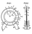
- the disk-shaped ceramic body 1 is provided on its two end faces 3 and 4 with coatings 5 and 6, for example made of stoving silver, which do not extend to the peripheral surface 2 of the body 1 and leave two free areas 13 and 14 between their edge and the peripheral surface.
- Annular current supply elements 7 and 8 are soldered in the center on both assignments 5 and 6, i.e. the center of the disk-shaped body 1 and the center of the annular current supply elements coincide.
- the radius Ra of the metallic, solderable coatings 5 and 6 is dimensioned such that a surface Fa of the coatings 5 and 6, which is located outside the current supply elements 7 and 8, results.
- the difference between the outer radius ra and the inner radius ri of the power supply element 7 and 8 determines on the one hand the width of the annular power supply elements and on the other hand the ratio between the outer circumference Ua and the inner circumference Ui thereof.
- the area Fa of the assignment 5 or 6 located outside the current supply element 7 or 8 should be in the same ratio to the inner area Fi as the outer circumference Ua. To the inner circumference Ui of the current supply element 7 or 8.
- the power supply elements 7 and 8 are provided with supply tabs 9 and 10, which are so far from the surface of the coatings 5 and 6 6 by kinks 11 and 12 on the outer circumference Ua of the power supply elements 7 and 8 that they clearances 17 and 18 respectively form, these spaces are not connected with solder.
- solder lugs 15 and 16 are provided, which are used to connect the feeder tabs to the fittings of the device, which with a varistor, as in the present case, or with a PTC resistor, an NTC resistor, or a ceramic Capacitor should be provided.
Landscapes
- Engineering & Computer Science (AREA)
- Microelectronics & Electronic Packaging (AREA)
- Power Engineering (AREA)
- Manufacturing & Machinery (AREA)
- Physics & Mathematics (AREA)
- Electromagnetism (AREA)
- Thermistors And Varistors (AREA)
- Details Of Resistors (AREA)
- Emergency Protection Circuit Devices (AREA)
Claims (6)

et que chaque élément d'amenée de courant (7, 8) est pourvu d'une patte d'amenée (9, 10) qui est écartée de la surface du revêtement (5, 6) par des repliages (11, 12) sur le pourtour extérieur (Ua) de l'élément d'amenée de courant (7, 8), avec formation d'un espace libre (17, 18), à tel point que la patte n'est pas soudée au revêtement (5, 6).
Priority Applications (1)
| Application Number | Priority Date | Filing Date | Title |
|---|---|---|---|
| AT87102591T ATE48921T1 (de) | 1986-04-23 | 1987-02-24 | Elektrisches bauelement mit hoher festigkeit bei beanspruchung durch temperaturwechsel und durch stossstroeme, insbesondere ein varistor. |
Applications Claiming Priority (2)
| Application Number | Priority Date | Filing Date | Title |
|---|---|---|---|
| DE3613787 | 1986-04-23 | ||
| DE3613787 | 1986-04-23 |
Publications (2)
| Publication Number | Publication Date |
|---|---|
| EP0243602A1 EP0243602A1 (fr) | 1987-11-04 |
| EP0243602B1 true EP0243602B1 (fr) | 1989-12-20 |
Family
ID=6299375
Family Applications (1)
| Application Number | Title | Priority Date | Filing Date |
|---|---|---|---|
| EP87102591A Expired EP0243602B1 (fr) | 1986-04-23 | 1987-02-24 | Composant électrique à plus grande rigidité à l'encontre de variations de température et d'impulsions de courant, en particulier une varistance |
Country Status (6)
| Country | Link |
|---|---|
| US (1) | US4714910A (fr) |
| EP (1) | EP0243602B1 (fr) |
| JP (1) | JPH088163B2 (fr) |
| AT (1) | ATE48921T1 (fr) |
| CA (1) | CA1264867A (fr) |
| DE (1) | DE3761236D1 (fr) |
Families Citing this family (9)
| Publication number | Priority date | Publication date | Assignee | Title |
|---|---|---|---|---|
| EP0315700B1 (fr) * | 1987-05-28 | 1994-01-05 | Matsushita Electric Industrial Co., Ltd. | Dispositif absorbeur de courants de choc |
| US5852397A (en) | 1992-07-09 | 1998-12-22 | Raychem Corporation | Electrical devices |
| EP0760157B1 (fr) | 1994-05-16 | 1998-08-26 | Raychem Corporation | Dispositifs electriques comprenant un element resistant ctp |
| US5691688A (en) * | 1994-07-20 | 1997-11-25 | Therm-O-Disc, Incorporated | PTC device |
| JP2000223359A (ja) * | 1999-01-29 | 2000-08-11 | Murata Mfg Co Ltd | セラミック電子部品 |
| US6640420B1 (en) | 1999-09-14 | 2003-11-04 | Tyco Electronics Corporation | Process for manufacturing a composite polymeric circuit protection device |
| US6854176B2 (en) | 1999-09-14 | 2005-02-15 | Tyco Electronics Corporation | Process for manufacturing a composite polymeric circuit protection device |
| DE10137873C1 (de) * | 2001-08-02 | 2002-10-17 | Epcos Ag | Elektrokeramisches Bauelement |
| CN112735823A (zh) * | 2019-10-14 | 2021-04-30 | 国网电力科学研究院武汉南瑞有限责任公司 | 多边形环状电容器引出焊片 |
Family Cites Families (9)
| Publication number | Priority date | Publication date | Assignee | Title |
|---|---|---|---|---|
| FR896326A (fr) * | 1942-07-29 | 1945-02-19 | Steatit Magnesia Ag | Amenée de courant pour condensateurs céramiques en forme de plaques circulaires |
| US3793604A (en) * | 1973-04-09 | 1974-02-19 | Gte Sylvania Inc | High strength electrical lead for disk type thermistors |
| US3959763A (en) * | 1975-04-17 | 1976-05-25 | General Signal Corporation | Four terminal varistor |
| CH607400A5 (fr) * | 1977-01-10 | 1978-12-15 | Cerberus Ag | |
| US4212045A (en) * | 1978-12-22 | 1980-07-08 | General Electric Company | Multi-terminal varistor configuration |
| JPS6048201U (ja) * | 1983-09-09 | 1985-04-04 | ティーディーケイ株式会社 | 正特性サ−ミスタ装置 |
| JPS6122307U (ja) * | 1984-07-17 | 1986-02-08 | ティーディーケイ株式会社 | 正特性サ−ミスタ |
| JPH039284Y2 (fr) * | 1984-09-25 | 1991-03-08 | ||
| DE8506668U1 (de) * | 1985-03-07 | 1986-04-10 | Siemens AG, 1000 Berlin und 8000 München | Elektrischer Widerstand mit negativem Temperaturkoeffizienten des Widerstandswertes |
-
1987
- 1987-02-24 DE DE8787102591T patent/DE3761236D1/de not_active Expired - Lifetime
- 1987-02-24 EP EP87102591A patent/EP0243602B1/fr not_active Expired
- 1987-02-24 AT AT87102591T patent/ATE48921T1/de not_active IP Right Cessation
- 1987-03-05 US US07/022,003 patent/US4714910A/en not_active Expired - Lifetime
- 1987-04-17 JP JP62096118A patent/JPH088163B2/ja not_active Expired - Lifetime
- 1987-04-21 CA CA000535074A patent/CA1264867A/fr not_active Expired - Lifetime
Also Published As
| Publication number | Publication date |
|---|---|
| DE3761236D1 (de) | 1990-01-25 |
| JPH088163B2 (ja) | 1996-01-29 |
| US4714910A (en) | 1987-12-22 |
| CA1264867A (fr) | 1990-01-23 |
| ATE48921T1 (de) | 1990-01-15 |
| JPS62266804A (ja) | 1987-11-19 |
| EP0243602A1 (fr) | 1987-11-04 |
Similar Documents
| Publication | Publication Date | Title |
|---|---|---|
| DE69221392T2 (de) | Verfahren zur Herstellung einer PTC-Anordnung | |
| DE3685849T2 (de) | Kaltleiteranordnungen auf basis von leitenden polymeren. | |
| EP0189087B1 (fr) | Résistance électrique dépendant de la tension (varistance) | |
| DE2235783C2 (de) | Metalloxid-Varistorelement | |
| DE3886898T2 (de) | Überspannungsableiter. | |
| DE3727014A1 (de) | Hochspannungskondensator | |
| DE3785946T2 (de) | Halbleiterbauelement aus positiver keramik. | |
| EP0243602B1 (fr) | Composant électrique à plus grande rigidité à l'encontre de variations de température et d'impulsions de courant, en particulier une varistance | |
| DE3638286A1 (de) | Elektrisches bauelement aus keramik mit mehrlagenmetallisierung und verfahren zu seiner herstellung | |
| DE2941196C2 (fr) | ||
| DE60030901T2 (de) | Chip-Vielschichtlaminat-Varistor | |
| DE2357127C3 (de) | Anordnung zur Funkenunterdrückung für einen Gleichstrommotor geringer Größe | |
| DE3421672A1 (de) | Wechsellastbestaendiges, schaltbares halbleiterbauelement | |
| DE102013106810A1 (de) | Verfahren zur Herstellung eines Vielschicht-Varistorbauelements und Vielschicht-Varistorbauelement | |
| DE2853134C2 (de) | Keramikvaristor | |
| DE1538526A1 (de) | UEberspannungsschutzvorrichtung fuer elektrische Bauelemente | |
| DE10061689A1 (de) | Kondensator | |
| DE10011009B4 (de) | Thermistor mit negativem Temperaturkoeffizient | |
| DE3509014A1 (de) | Elektrisches bauelement mit einem keramisch hergestellten koerper und gegenpoligen kontaktbelegungen | |
| DE3050770C2 (de) | Verfahren zur Herstellung eines Varistors | |
| DE3022489C2 (fr) | ||
| DE8611209U1 (de) | Elektrisches Bauelement mit hoher Festigkeit bei Beanspruchung durch Temperaturwechsel und durch Stoßströme, insbesondere ein Varistor | |
| WO2003028185A1 (fr) | Composant electrique | |
| EP0193854B1 (fr) | Résistance électrique à coefficient de température négatif et son procédé de fabrication | |
| EP0827160A1 (fr) | Composant électro-céramique multicouche et procédé de fabrication |
Legal Events
| Date | Code | Title | Description |
|---|---|---|---|
| PUAI | Public reference made under article 153(3) epc to a published international application that has entered the european phase |
Free format text: ORIGINAL CODE: 0009012 |
|
| AK | Designated contracting states |
Kind code of ref document: A1 Designated state(s): AT CH DE FR GB IT LI NL SE |
|
| 17P | Request for examination filed |
Effective date: 19871204 |
|
| 17Q | First examination report despatched |
Effective date: 19890207 |
|
| GRAA | (expected) grant |
Free format text: ORIGINAL CODE: 0009210 |
|
| AK | Designated contracting states |
Kind code of ref document: B1 Designated state(s): AT CH DE FR GB IT LI NL SE |
|
| REF | Corresponds to: |
Ref document number: 48921 Country of ref document: AT Date of ref document: 19900115 Kind code of ref document: T |
|
| REF | Corresponds to: |
Ref document number: 3761236 Country of ref document: DE Date of ref document: 19900125 |
|
| ET | Fr: translation filed | ||
| ITF | It: translation for a ep patent filed | ||
| GBT | Gb: translation of ep patent filed (gb section 77(6)(a)/1977) | ||
| PLBE | No opposition filed within time limit |
Free format text: ORIGINAL CODE: 0009261 |
|
| STAA | Information on the status of an ep patent application or granted ep patent |
Free format text: STATUS: NO OPPOSITION FILED WITHIN TIME LIMIT |
|
| 26N | No opposition filed | ||
| ITTA | It: last paid annual fee | ||
| EAL | Se: european patent in force in sweden |
Ref document number: 87102591.2 |
|
| REG | Reference to a national code |
Ref country code: CH Ref legal event code: NV Representative=s name: E. BLUM & CO. PATENTANWAELTE |
|
| REG | Reference to a national code |
Ref country code: CH Ref legal event code: PUE Owner name: SIEMENS AKTIENGESELLSCHAFT BERLIN UND MUENCHEN -DA |
|
| REG | Reference to a national code |
Ref country code: FR Ref legal event code: TP |
|
| REG | Reference to a national code |
Ref country code: GB Ref legal event code: IF02 |
|
| NLS | Nl: assignments of ep-patents |
Owner name: EPCOS AG |
|
| PGFP | Annual fee paid to national office [announced via postgrant information from national office to epo] |
Ref country code: AT Payment date: 20030203 Year of fee payment: 17 Ref country code: SE Payment date: 20030203 Year of fee payment: 17 Ref country code: CH Payment date: 20030203 Year of fee payment: 17 Ref country code: NL Payment date: 20030203 Year of fee payment: 17 |
|
| PG25 | Lapsed in a contracting state [announced via postgrant information from national office to epo] |
Ref country code: AT Free format text: LAPSE BECAUSE OF NON-PAYMENT OF DUE FEES Effective date: 20040224 |
|
| PG25 | Lapsed in a contracting state [announced via postgrant information from national office to epo] |
Ref country code: SE Free format text: LAPSE BECAUSE OF NON-PAYMENT OF DUE FEES Effective date: 20040225 |
|
| PG25 | Lapsed in a contracting state [announced via postgrant information from national office to epo] |
Ref country code: LI Free format text: LAPSE BECAUSE OF NON-PAYMENT OF DUE FEES Effective date: 20040229 Ref country code: CH Free format text: LAPSE BECAUSE OF NON-PAYMENT OF DUE FEES Effective date: 20040229 |
|
| PG25 | Lapsed in a contracting state [announced via postgrant information from national office to epo] |
Ref country code: NL Free format text: LAPSE BECAUSE OF NON-PAYMENT OF DUE FEES Effective date: 20040901 |
|
| EUG | Se: european patent has lapsed | ||
| REG | Reference to a national code |
Ref country code: CH Ref legal event code: PL |
|
| NLV4 | Nl: lapsed or anulled due to non-payment of the annual fee |
Effective date: 20040901 |
|
| PGFP | Annual fee paid to national office [announced via postgrant information from national office to epo] |
Ref country code: FR Payment date: 20060217 Year of fee payment: 20 |
|
| PGFP | Annual fee paid to national office [announced via postgrant information from national office to epo] |
Ref country code: GB Payment date: 20060223 Year of fee payment: 20 |
|
| PGFP | Annual fee paid to national office [announced via postgrant information from national office to epo] |
Ref country code: IT Payment date: 20060228 Year of fee payment: 20 |
|
| PGFP | Annual fee paid to national office [announced via postgrant information from national office to epo] |
Ref country code: DE Payment date: 20060331 Year of fee payment: 20 |
|
| PG25 | Lapsed in a contracting state [announced via postgrant information from national office to epo] |
Ref country code: GB Free format text: LAPSE BECAUSE OF EXPIRATION OF PROTECTION Effective date: 20070223 |
|
| REG | Reference to a national code |
Ref country code: GB Ref legal event code: PE20 |