EP0242255A2 - Schaltungsprüfsystem - Google Patents
Schaltungsprüfsystem Download PDFInfo
- Publication number
- EP0242255A2 EP0242255A2 EP87400637A EP87400637A EP0242255A2 EP 0242255 A2 EP0242255 A2 EP 0242255A2 EP 87400637 A EP87400637 A EP 87400637A EP 87400637 A EP87400637 A EP 87400637A EP 0242255 A2 EP0242255 A2 EP 0242255A2
- Authority
- EP
- European Patent Office
- Prior art keywords
- driver
- response
- signals
- stimulus
- tested
- Prior art date
- Legal status (The legal status is an assumption and is not a legal conclusion. Google has not performed a legal analysis and makes no representation as to the accuracy of the status listed.)
- Withdrawn
Links
Images


Classifications
-
- G—PHYSICS
- G01—MEASURING; TESTING
- G01R—MEASURING ELECTRIC VARIABLES; MEASURING MAGNETIC VARIABLES
- G01R31/00—Arrangements for testing electric properties; Arrangements for locating electric faults; Arrangements for electrical testing characterised by what is being tested not provided for elsewhere
- G01R31/28—Testing of electronic circuits, e.g. by signal tracer
- G01R31/317—Testing of digital circuits
- G01R31/3181—Functional testing
- G01R31/319—Tester hardware, i.e. output processing circuits
- G01R31/31917—Stimuli generation or application of test patterns to the device under test [DUT]
- G01R31/31919—Storing and outputting test patterns
-
- G—PHYSICS
- G01—MEASURING; TESTING
- G01R—MEASURING ELECTRIC VARIABLES; MEASURING MAGNETIC VARIABLES
- G01R31/00—Arrangements for testing electric properties; Arrangements for locating electric faults; Arrangements for electrical testing characterised by what is being tested not provided for elsewhere
- G01R31/28—Testing of electronic circuits, e.g. by signal tracer
- G01R31/317—Testing of digital circuits
- G01R31/3181—Functional testing
- G01R31/319—Tester hardware, i.e. output processing circuits
- G01R31/31903—Tester hardware, i.e. output processing circuits tester configuration
- G01R31/31905—Interface with the device under test [DUT], e.g. arrangements between the test head and the DUT, mechanical aspects, fixture
Definitions
- the present invention relates to the field of circuit testers and particularly to systems for testing digital integrated circuits.
- U.S. Patent No. 4,066,882 to Esposito shows a digital stimulus generating and response measuring system.
- U.S. Patent No. 4,168,796 to Fulks et al shows a portable tester for testing a variety of printed circuit boards without utilizing specialized adaptor boards for rerouting input test signals and supply voltages from the tester to various pins of the board under test.
- U.S. Patent No. 4,194,113 to Fulks et al shows a method and apparatus for isolating faults in digital printed circuit boards under test.
- U.S. Patent No. 4,308,615 to Koegel et al discloses an apparatus for use in automatic testing of elements in data processing systems.
- One object of the present invention is to provide a device which can be used in combination with a conventional personal computer to provide a highly sophisticated and versatile testing system for digital circuits.
- Another object of the present invention is to provide a system for testing a plurality of different integrated circuits without the need for a special wiring harness for each circuit tested.
- Yet another object of the present invention is to provide a testing system for digital circuits which is capable of providing stimulus signals to the device under test and monitoring response signals to detect errors using a minimum number of components.
- Another object of the present invention is to provide a testing system for digital circuits in which the functioning of the device is modified automatically to compensate for different loading on channels being stimulated.
- the system of the present invention comprises structure for providing connections to a plurality of inputs of a circuit to be tested and a device for storing test vectors comprising data representing stimulus signals to be applied through the connections and response signals to be sensed through the connections.
- the invention applies the stored test vectors to the connections using a driver associated with each input of the circuit to be tested.
- Each driver has an output capable of assuming a high state, a low state, or a floating state.
- a driver control receives data indicative of the test vectors and controls the driver to assume a high or low output state in response to stimulus signal data, and to assume a floating state in response to response signal data.
- the response signals from the connections are compared to response signal data to determine a fault.
- the driver may be a tri-statable device having a data input for receiving stimulus data and a control input for causing the driver output to float or to assume a high or low state in response to the driver data input.
- the driver control comprises a register for storing stimulus and response signal data and connected to the data input of the driver.
- the driver control comprises a status register connected to the control input for applying control data for causing said driver output to float or respond to said driver data input.
- the comparison between a response signal from the device under test and response signal data may be performed in a comparator having a first input connected to the output of the register for storing stimulus and response data, and having a second input connected to the circuit to be tested.
- an adjustable clock may be provided for controlling the timing between the application of stimulus data to the driver data input, and application of control data from the status register to the driver.
- Figure 1 shows a digital testing apparatus 10 which comprises a housing 11 having a rocker-type on/off switch 12.
- an indicator light 14 for indicating when the power to the unit has been turned on.
- a reset switch 15 for placing all of the tri-statable devices of the unit (to be discussed below) in their tri-state condition, ready to accept programming of new test data.
- Positive and negative terminals 12 and 12 ⁇ of a five volt power supply are also provided for supplying power to a device under test.
- the front panel of housing 11 contains four rows of 32 pins marked as channels 1-4. The pins are also marked as to their sequential position in the row for pins 1, 10, 24 and 32. Each pin is individually accessible using a spring loaded test probe or jumper wires fitted with square pin female connector hardware.
- a 64 pin zero insertion force socket 16 is provided for connection to channels 2 and 3. This socket may be a conventional socket as provided by Textool. Socket 16 is fitted over the pins of channels 2 and 3 and may be actuated by movement of a lever 17.
- pins 18 of channel 1 and pins 20 of channel 4 remain exposed for connection to ribbon cable, spring loaded test probes or the like.
- a 25 pin D-type connector port 21 is provided for connection to a personal computer by cable.
- a second testing apparatus 22 has a housing 23 and contains a single zero insertion force socket 24 operated by lever 26. Testing apparatus 22 is slightly larger than testing apparatus 10 and is more versatile, as will be discussed below.
- Adaptor cards are provided for connection to zero insertion force sockets 16 or 24 to enable testers 10 and 22 to easily test 3/10" or 6/10" dual in-line packs or to test circuits contained in plastic leadless chip carriers.
- FIG 3 shows the testing apparatus 10 connected to a personal computer 28.
- Computer 28 may be any conventional computer such as an IBM PC, PCXT or PCAT.
- Cable 29 connects the computer 28 to the testing apparatus 10.
- Testing apparatus 10 has a plurality of logic circuits 30.
- One logic circuit is associated with each of the pins of the channels 1, 2, 3 and 4. Only one logic circuit 30 is shown in detail in Figure 3.
- Cable 29 contains a bi-directional data line 32, a stimulus load timing line 34, a status load timing line 36, a clock line 38, and a response status line 56.
- the bi-directional data line 32 is connected to the data input of flip-flop 40 which has an output connected to the data input of a flip-flop 42.
- Line 32 is also connected to the input of a flip-flop 44 which has its output connected to the input of a flip-flop 46.
- the output of flip-flop 42 connects to the data input of a tri-statable driver 48 and the output flip-flop 46 is connected to a control input of tri-statable driver 48.
- the output of driver 48 is connected to output line 50 which is connected to one of the pins of channels 1, 2, 3 or 4.
- Tri-statable driver 48 can be any conventional driver which has a control input determining whether its output is floating or responsive to the input. In the case of tri-statable driver 48, if an output of flip-flop 46 is high, the output on line 50 of driver 48 responds to the input of driver 48 from flip-flop 42. Thus, if flip-flop 42 has high output, the signal on line 50 is also high. If the output of flip-flop 42 is low, the output on line 50 is also a low. If the output of flip-flop 46 is low, the output of driver 48 on line 50 is floating.
- Line 50 is bi-directional so that both stimulus and response signals may be present.
- Line 50 leads to the input of a second tri-statable device 54 which has its output on line 32 and has its control input connected to line 56.
- a conventional test vector file for the device under test is loaded into computer 28 and used to drive circuit 30.
- Flip-flops 40 and 42 act as a stimulus register for providing stimulus signals to tri-statable device 48.
- Flip-flops 44 and 46 form a status register for storing control signals for tri-statable device 48.
- Computer 28 loads flip-flops 40 and 44 with the first stimulus and status signals, respectively, by clocking the appropriate data into flip-flops 40 and 44 using timing lines 34 and 36. Line 38 is then driven high to transfer the data from flip-flops 40 and 44 to flip-flops 42 and 46.
- circuit 30 If circuit 30 is to be used as a stimulus channel, the output from flip-flop 46 at this time will be a one signal causing driver 48 to drive line 50 with the same signal as is output from flip-flop 42. At the same time, line 56 is driven low by computer 28 to enable line 32 to be under the control of the computer in order for new data to be presented to flip-flops 40 and 44.
- line 50 is to receive a response from the device under test
- the output of flip-flop 46 is driven low so as to enable line 50 to be under the control of the device under test.
- line 56 is driven high by the computer so that the response signal on line 50 is transferred to line 32.
- the software used to drive a particular circuit 30, could easily be generated by one of ordinary skill in the art.
- the software reads the vector for the test pin connected to that circuit 30 and drives the circuit so as to provide either a stimulus whereby line 50 is driven to the level of the stimulus signal, or to transmit a response from line 50 to the computer through line 32.
- Figure 4 shows the logic circuit for testing apparatus 22.
- a single circuit 58 is disclosed, it being understood that a separate circuit 58 is provided for each socket contact of socket 24.
- Figure 4 shows timing circuitry 60 which is common to all of the logic circuits 58.
- Logic circuit 58 is connected to a mask data line 62 which is connected to an input of a shift register 64 which stores mask information.
- the output of shift register 64 is connected to a line 66 which is also connected to one input of an AND gate 74.
- An error data line 68 is connected between an error shift register 70 and the host computer 28.
- the input of error shift register 70 is received on line 72 from the output of AND gate 74.
- a second input to AND gate 74 is received from a comparator 76 on line 78.
- a stimulus/response data line 80 is connected from computer 28 to the input of a stimulus/response shift register 82.
- the output of shift register 82 is passed along line 84 to the input of tri-statable device 86.
- Line 84 is also connected to one input of comparator 76.
- the output of tri-statable driver 86 is connected to line 88 which leads to one pin of the device under test 90 and which also leads to a second input of comparator 76.
- a status data line 92 is connected from host computer 28 to a status shift register 94.
- the output of register 94 is connected to a line 96 which is also connected to the control input of tri-statable driver 86.
- the timing circuitry 60 contains an oscillator 98 which has its output connected to a control circuit 100.
- Circuit 100 operates under direct control of the computer through a line 102.
- the output of control circuit 100 is a clock signal on line 104.
- Control circuit 100 contains essentially a programmable divider for controlling the frequency of the clock signal on line 104 as well as the number of clock pulses output onto line 104.
- Line 104 is connected to the input of a delay module 118.
- Module 118 delays any clock pulses received on line 104 by an amount commanded by the computer 28 through line 120 and passes the delayed clock pulses to a compare clock line 122. Accordingly, the pulses on clock line 104 and the compare clock pulses on line 122 are provided to each of the logic circuits 58.
- the clock pulses on line 104 are provided to the clock input of shift register 64 and shift register 70.
- the clock pulses on line 104 are also provided to a delay module 106 which delays these pulses by an amount controlled by computer 28 through line 108, and passes the delay clock pulses through a line 110 to the clock input of shift register 82.
- the clock pulses on line 104 are also provided to a delay module 104 which is under the control of computer 28 through a line 114.
- the delayed pulses from module 112 are passed through line 116 to the clock input of shift register 94.
- the compare clock pulses on line 122 are passed to the control input of comparator 76. Accordingly, the comparator 76 is operative to compare the signals on lines 84 and 88 at the active edge of each compare clock pulse received on line 122.
- the stimulus/response register 82 and status register 94 are loaded by the computer.
- the stimulus clock delay 106 is controlled to be less than the status clock delay 112 so that a signal from register 82 is provided on line 84 before the control input of tri-statable driver 86 receives a signal from status register 94. If the signal from register 82 is intended to be a stimulus signal, the output of status register 94 will be high causing the signal on line 84 to be transmitted to line 88 and to the device under test 90. In this case, at the leading edge of the compare clock pulse 122, the stimulus signal on line 84 is compared to the signal on line 88 to ensure that the proper stimulus signal is provided to the device under test 90.
- logic circuit 58 If logic circuit 58 is to receive a response from device under test 90, the status register 94 outputs a low level signal. In this case, the response from the device under test 90 is transmitted along line 88 to comparator 76 and the response data signal from register 82 is transmitted along line 84 to comparator 76. Upon the rising edge of a compare clock pulse, comparator 76 compares the response signal with the response data signal and outputs the result on line 78.
- mask register 64 will provide a low level signal to AND gate 74 so as to block the result of the comparison on line 78 from reaching error register 70. In this situation, no errors will be detected. In the case where errors are to be detected, the mask register is loaded with ones so that gate 74 will always pass an error signal when it is generated.
- the programmable delay modules 106, 112 and 118 enable the relationship between the clock pulses on line 104, the stimulus clock pulses on line 110, the status clock pulses on line 116, and the compare clock pulses on line 122 to be altered within limits.
- the clock pulses 104 will always occur first so that any mask data from register 64 will be provided to AND gate 74 and any errors produced by a previous comparison will be entered into register 70.
- the stimulus and status clocks will then occur to set the state of driver 86 and provide the stimulus or response data from register 82.
- the compare clock will occur last to ensure that the signals on lines 84 and 88 are valid before a comparison is carried out.
- the result of the comparison will then be entered into error register 70 upon the occurrence of the next clock pulse.
- the variability of the delays solves several problems. As the loading of a given stimulus channel is increased, the propagation delay generated by tri-statable driver 86 increases. Therefore, the device under test receives this stimulus at a later time. This has the effect of removing some of the time that was alloted for the device under test response pins to settle to their valid states. By moving the compare clock pulses on line 122 to a point in time where no errors occur on the stimulus pins, the effect of loading can be nullified. Accordingly, differences in part to part delay characteristics exhibited by the components of circuit 58 can be nullified. This provides concurrent stimuli on all channels driving the device under test. Also, differences in stimuli delay due to non-uniform capacitive loading of the device under test may be nullified within limits. This is the case where one or more pins of the device under test present a greater load than the others. The result is stimulus skew that may be nullified by skewing stimulus and status clocks.
- variable delays allow the user to skew stimuli by a known amount in the interest of checking the characteristics of the device under test such as data setup and hold times.
- the present invention includes an autocalibration program for setting the delays 106, 112 and 118 of the stimulus channels.
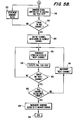
- Figures 5a and 5b show a flow chart for the autocalibration program.
- the program is entered at step 128 and control passes to step 130 where the test vector file for the device under test is read.
- the input statement of this file identifies the stimulus pins of the device under test.
- step 132 the software loads the stimulus/response register 82 with data from the corresponding column of the test vector file for each stimulus channel.
- step 134 the status register 94 is loaded with 1's to cause each stimulus channel to drive the device under test.
- step 136 the mask register 64 for each stimulus channel is loaded with 1's so that no errors are masked in the stimulus channels.
- step 138 the mask register 64 of each response channel is loaded with 0's to mask all errors in the response channels.
- step 140 programmable control block 100 is set to provide a clock signal at a relatively low frequency. This allows for a large initial setting of delay 118 which is common to all channels.
- step 142 delay 106 for the stimulus clock of each stimulus channel is set to a minimum delay so that the stimulus data is provided relatively quickly after the clock signal occurs.
- step 144 the status clock delay 112 is set to some initial value for each stimulus channel. The initial value may be the same delay time as set in delay 106.
- step 146 the compare clock delay in block 118 is set at a initial value which is relatively high so that the compare clock occurs at a point in time where no error signal due to loading by the device under test is expected.
- step 150 the contents of the error register 70 are clocked into the computer to determine whether any error has occurred in a stimulus channel. If no error has occurred, control passes to step 152 where the delay set in compare clock delay module 118 is decremented by a preset amount. Control then passes to step 148 again where another test step is executed. This procedure continues until an error is developed in a stimulus channel. Step 154 then defines this channel as the slowest channel; in other words, the channel having the greatest loading effect on its tri-statable driver 86.
- step 158 one test step is executed and in step 160, the error register 70 of the "next channel" is accessed to determine whether an error has occurred. If no error has occurred, control passes to step 156. Steps 156 and 158 are repeated until an error has occurred. In this case, control passes from 160 to step 162 where the computer checks to see whether all channels have been tested until an error has occurred. If not, control passes to step 164 where the "next channel” is incremented. These steps are repeated until each channel registers an error.
- step 166 control passes to step 166 where the compare clock delay 118 is incremented to eliminate all errors. Accordingly, this procedure sets the compare clock delay 118 at a "compare reference" for the device under test. This is the smallest value that can be used by the compare clock and have no errors generated by any of the stimulus channels. Also, the stimulus clocks of the channels have now been set such that a valid signal on line 88 of each channel will have been attained at approximately the same time. Thus, concurrent stimuli are provided on all channels driving the device under test.
- the present invention includes adaptor cards such as those shown in Figures 6 and 7.
- Figure 6 shows a top plan schematic view of an adaptor card designed to fit into the socket 16 of testing apparatus 10.
- a similar adaptor card can be used in socket 24 of testing apparatus 22.
- Adaptor card 170 includes zero insertion force socket 172 which can be a Textool Model 220-3342 socket. This socket will receive 3/10" dual in-line packs. Socket 172 is mounted directly on a printed circuit board 171 of the adaptor card 170.
- a second zero insertion force socket 174 is also mounted on printed circuit board 171. Socket 174 can receive 6/10" dual in-line packages.
- a plurality of pins 176 extend downwardly from the printed circuit board 171 and align with the socket contact of socket 16 forming channel 2 of the testing apparatus 10 shown in Figure 1.
- a plurality of pins 178 extend downwardly from printed circuit board 170 to align with the socket contacts forming channel 3 of the socket 16. Accordingly, adaptor 170 can be plugged directly into socket 16 of Figure 1.
- the socket contacts of sockets 172 and 174 are connected, respectively, to pins 176 and 178.
- a plurality of upwardly extending pins 180 and 182 are provided on the printed circuit board 171. These pins are connected, respectively, to the pins 176 and 178 through 100 ohm series damping resistors 184. Pins 180 and 182 can be connected to a ribbon cable, autoprober or the like.
- Figure 7 shows a second adaptor card 186 which can be used to test device packages in 28 pin plastic leadless chip carriers.
- a mount such as a Textool Model 228-5523 is directly attached to the printed circuit board at position 188.
- the leads from this mount are connected to downwardly extending pins 190 and 192.
- a plurality of upwardly extending pins 194 is provided.
- a jumper in the form of a ribbon cable is connected from pins 194 to four of the pins 20 of channel 4 of the testing apparatus 10 of Figure 1.
- a software file must be created indicating where the device under test is connected to the testing apparatus.
- the discussion relates to testing apparatus 10 although the discussion is equally applicable to testing apparatus 22.
- sockets 172 and 174 are available for use.
- Socket 172 can handle 6, 8, 14, 16, 18 and 20 pin dual in-line parts. Assuming that the user is testing an 8 pin dual in-line part, the part will be inserted into the top of the 20 pin socket 172 and will use the top four pins on the left hand side of the socket, and the top four pins on the right hand side of the socket.
- Adaptor card 170 uses channel 2 for all of the pins on the 20 pin socket 172.
- the pin numbering is counterclockwise beginning with channel 2, pin 1 and ending with channel 2, pin 20.
- the part will use on the left hand side of the socket channel 2, pin 1; channel 2, pin 2; channel 2, pin 3; and channel 2, pin 4.
- On the right hand side of the socket channel 2, pin 17; channel 2, pin 18; channel 2, pin 19; and channel 2, pin 20 will be used.
- the user will indicate this sequence in an appropriate software file for the computer to read.
- the file contains many sets of data, each labeled by an identifying header.
- the data file can be identified by the key word PKGNAME and something to identify the particular part being tested such as, "X-18 pin,".
- the data file would appear as follows: PKGNAMEX18PIN 2-1 2-2 2-3 2-4 2-17 2-18 2-19 2-20
- the vector file for the device under test is formatted with one column for each pin of the device.
- the columns are then associated with the pins of channels 1 through 4 of apparatus 10 using the above file.
- a similar file is produced and stored for each device to be tested. In this manner, it is not necessary to hard wire a separate test setup for each part to be tested.
- the testing apparatus, the adaptor card and software can easily be modified to handle any device to be tested.
Landscapes
- Engineering & Computer Science (AREA)
- General Engineering & Computer Science (AREA)
- Physics & Mathematics (AREA)
- General Physics & Mathematics (AREA)
- Tests Of Electronic Circuits (AREA)
Applications Claiming Priority (2)
| Application Number | Priority Date | Filing Date | Title |
|---|---|---|---|
| US06/850,058 US4771428A (en) | 1986-04-10 | 1986-04-10 | Circuit testing system |
| US850058 | 1997-05-02 |
Publications (2)
| Publication Number | Publication Date |
|---|---|
| EP0242255A2 true EP0242255A2 (de) | 1987-10-21 |
| EP0242255A3 EP0242255A3 (de) | 1989-08-23 |
Family
ID=25307163
Family Applications (1)
| Application Number | Title | Priority Date | Filing Date |
|---|---|---|---|
| EP87400637A Withdrawn EP0242255A3 (de) | 1986-04-10 | 1987-03-23 | Schaltungsprüfsystem |
Country Status (3)
| Country | Link |
|---|---|
| US (1) | US4771428A (de) |
| EP (1) | EP0242255A3 (de) |
| JP (1) | JPS6333677A (de) |
Cited By (2)
| Publication number | Priority date | Publication date | Assignee | Title |
|---|---|---|---|---|
| WO1990002926A1 (en) * | 1988-09-12 | 1990-03-22 | Kjell Moum | An instrument for checking the operational state of an ic-circuit |
| DE9108852U1 (de) * | 1991-07-18 | 1991-10-17 | Keitel, Stefan, Dipl.-Ing. M.Phil./Brunel Univ., 6460 Gelnhausen | RS - 232 Schnittstellen - Test - Adapter |
Families Citing this family (20)
| Publication number | Priority date | Publication date | Assignee | Title |
|---|---|---|---|---|
| US5426767A (en) * | 1987-08-03 | 1995-06-20 | Compaq Computer Corporation | Method for distinguishing between a 286-type central processing unit and a 386-type central processing unit |
| US4878179A (en) * | 1987-11-12 | 1989-10-31 | Rockwell International Corporation | Interactive diagnostic methodology and apparatus for microelectronic devices |
| US4907230A (en) * | 1988-02-29 | 1990-03-06 | Rik Heller | Apparatus and method for testing printed circuit boards and their components |
| US4937765A (en) * | 1988-07-29 | 1990-06-26 | Mentor Graphics Corporation | Method and apparatus for estimating fault coverage |
| US5369593A (en) * | 1989-05-31 | 1994-11-29 | Synopsys Inc. | System for and method of connecting a hardware modeling element to a hardware modeling system |
| US5353243A (en) * | 1989-05-31 | 1994-10-04 | Synopsys Inc. | Hardware modeling system and method of use |
| US4985672A (en) * | 1989-12-11 | 1991-01-15 | Advantest Corporation | Test equipment for a low current IC |
| US5446742A (en) * | 1990-08-01 | 1995-08-29 | Zilog, Inc. | Techniques for developing integrated circuit test programs and their use in testing actual circuits |
| US5256963A (en) * | 1990-11-02 | 1993-10-26 | Micron Technology Inc. | Digital testing for high-impedance states in digital electronic circuits |
| US5196788A (en) * | 1991-07-03 | 1993-03-23 | The United States Of America As Represented By The Secretary Of The Navy | Self-contained functional test apparatus for modular circuit cards |
| US5423050A (en) * | 1991-11-27 | 1995-06-06 | Ncr Corporation | Intermodule test across system bus utilizing serial test bus |
| JP2708314B2 (ja) * | 1992-04-09 | 1998-02-04 | 三菱電機株式会社 | 論理シミュレーション装置 |
| EP0578858A1 (de) * | 1992-07-17 | 1994-01-19 | International Business Machines Corporation | AC-Verbindungsprüfung für integrierte Schaltungsbausteine |
| EP0642083A1 (de) * | 1993-09-04 | 1995-03-08 | International Business Machines Corporation | Prüfschaltkreis und Verfahren zum Prüfen von Chipverbindungen |
| JP3124417B2 (ja) * | 1993-07-13 | 2001-01-15 | 三菱電機株式会社 | 論理シミュレーションシステム及び論理シミュレーション方法 |
| US6055661A (en) * | 1994-06-13 | 2000-04-25 | Luk; Fong | System configuration and methods for on-the-fly testing of integrated circuits |
| US5673295A (en) * | 1995-04-13 | 1997-09-30 | Synopsis, Incorporated | Method and apparatus for generating and synchronizing a plurality of digital signals |
| US6088756A (en) * | 1998-09-29 | 2000-07-11 | International Business Machines Corporation | Five state bus driver having both voltage and current source modes of operation |
| JP4272726B2 (ja) * | 1998-10-08 | 2009-06-03 | 株式会社アドバンテスト | Ic試験方法及び装置 |
| US7174492B1 (en) * | 2001-04-12 | 2007-02-06 | Cisco Technology, Inc. | AC coupled line testing using boundary scan test methodology |
Citations (4)
| Publication number | Priority date | Publication date | Assignee | Title |
|---|---|---|---|---|
| US4066882A (en) * | 1976-08-16 | 1978-01-03 | Grumman Aerospace Corporation | Digital stimulus generating and response measuring means |
| GB1582927A (en) * | 1977-03-22 | 1981-01-14 | Bendix Corp | Portable circuit tester |
| GB2129571A (en) * | 1982-10-28 | 1984-05-16 | Tektronix Inc | Method and apparatus for synthesizing a drive signal for active ic testing |
| US4517661A (en) * | 1981-07-16 | 1985-05-14 | International Business Machines Corporation | Programmable chip tester having plural pin unit buffers which each store sufficient test data for independent operations by each pin unit |
Family Cites Families (10)
| Publication number | Priority date | Publication date | Assignee | Title |
|---|---|---|---|---|
| US4055801A (en) * | 1970-08-18 | 1977-10-25 | Pike Harold L | Automatic electronic test equipment and method |
| US3976940A (en) * | 1975-02-25 | 1976-08-24 | Fairchild Camera And Instrument Corporation | Testing circuit |
| US4125763A (en) * | 1977-07-15 | 1978-11-14 | Fluke Trendar Corporation | Automatic tester for microprocessor board |
| US4168527A (en) * | 1978-02-17 | 1979-09-18 | Winkler Dean A | Analog and digital circuit tester |
| US4168796A (en) * | 1978-04-13 | 1979-09-25 | Ncr Corporation | Tester with driver/sensor circuit having programmable termination devices |
| US4194113A (en) * | 1978-04-13 | 1980-03-18 | Ncr Corporation | Method and apparatus for isolating faults in a logic circuit |
| US4308615A (en) * | 1979-09-17 | 1981-12-29 | Honeywell Information Systems Inc. | Microprocessor based maintenance system |
| JPS5832178A (ja) * | 1981-08-19 | 1983-02-25 | Advantest Corp | Icテスタ |
| US4433414A (en) * | 1981-09-30 | 1984-02-21 | Fairchild Camera And Instrument Corporation | Digital tester local memory data storage system |
| US4646299A (en) * | 1983-08-01 | 1987-02-24 | Fairchild Semiconductor Corporation | Method and apparatus for applying and monitoring programmed test signals during automated testing of electronic circuits |
-
1986
- 1986-04-10 US US06/850,058 patent/US4771428A/en not_active Expired - Fee Related
-
1987
- 1987-03-23 EP EP87400637A patent/EP0242255A3/de not_active Withdrawn
- 1987-04-10 JP JP62087214A patent/JPS6333677A/ja active Pending
Patent Citations (4)
| Publication number | Priority date | Publication date | Assignee | Title |
|---|---|---|---|---|
| US4066882A (en) * | 1976-08-16 | 1978-01-03 | Grumman Aerospace Corporation | Digital stimulus generating and response measuring means |
| GB1582927A (en) * | 1977-03-22 | 1981-01-14 | Bendix Corp | Portable circuit tester |
| US4517661A (en) * | 1981-07-16 | 1985-05-14 | International Business Machines Corporation | Programmable chip tester having plural pin unit buffers which each store sufficient test data for independent operations by each pin unit |
| GB2129571A (en) * | 1982-10-28 | 1984-05-16 | Tektronix Inc | Method and apparatus for synthesizing a drive signal for active ic testing |
Non-Patent Citations (3)
| Title |
|---|
| ELEKTRONIK, vol. 34, no. 5, March 1985, pages 103-106, Munich, DE; R. POSTL: "Automatisches Testen der dynamischen Parameter digitaler Bauelemente" * |
| IEE INTERNATIONAL AUTOMATIC TESTING CONFERENCE, 12th-14th October 1982, pages 308-313, IEEE, Dayton, Ohio, US; R.W. TUCKER et al.: "Emphasizing flexibility in a digital test unit architecture" * |
| IEEE INTERNATIONAL TEST CONFERENCE, 15th-18th November 1982, pages 299-307, IEEE, Piscataway, New York, US; W.J. HORTH et al.: "Microelectronic device electrical test implementation problems on automated test equipment" * |
Cited By (3)
| Publication number | Priority date | Publication date | Assignee | Title |
|---|---|---|---|---|
| WO1990002926A1 (en) * | 1988-09-12 | 1990-03-22 | Kjell Moum | An instrument for checking the operational state of an ic-circuit |
| US5130648A (en) * | 1988-09-12 | 1992-07-14 | Kjell Moum | Instrument for checking the operational state of an ic-circuit |
| DE9108852U1 (de) * | 1991-07-18 | 1991-10-17 | Keitel, Stefan, Dipl.-Ing. M.Phil./Brunel Univ., 6460 Gelnhausen | RS - 232 Schnittstellen - Test - Adapter |
Also Published As
| Publication number | Publication date |
|---|---|
| EP0242255A3 (de) | 1989-08-23 |
| JPS6333677A (ja) | 1988-02-13 |
| US4771428A (en) | 1988-09-13 |
Similar Documents
| Publication | Publication Date | Title |
|---|---|---|
| US4771428A (en) | Circuit testing system | |
| US4718064A (en) | Automatic test system | |
| US4517512A (en) | Integrated circuit test apparatus test head | |
| US6016563A (en) | Method and apparatus for testing a logic design of a programmable logic device | |
| US6178526B1 (en) | Testing memory modules with a PC motherboard attached to a memory-module handler by a solder-side adaptor board | |
| US5243274A (en) | Asic tester | |
| US7356742B2 (en) | Method and apparatus for testing a memory device in quasi-operating conditions | |
| US5436554A (en) | Computer controlled cable tester | |
| KR890004450B1 (ko) | 검사 벡터 인덱싱 방법 및 장치 | |
| US4196386A (en) | Method and portable apparatus for testing digital printed circuit boards | |
| US5003156A (en) | Dual configuration connector port for burn-in systems | |
| US6369601B1 (en) | Method of measuring a propagation delay time through a transmission path in a semiconductor integrated circuit testing apparatus and semiconductor integrated circuit testing apparatus using the same | |
| US4760329A (en) | Programmable tester with bubble memory | |
| US6255843B1 (en) | Semiconductor integrated circuit testing apparatus and composite semiconductor integrated circuit testing apparatus | |
| US4485472A (en) | Testable interface circuit | |
| US4174805A (en) | Method and apparatus for transmitting data to a predefined destination bus | |
| WO2006071668A2 (en) | Pin electronics with high voltage functionality | |
| US6901541B2 (en) | Memory testing method and apparatus | |
| EP0157028B1 (de) | Programmierbares Prüfgerät | |
| US4779042A (en) | Computer-aided probe with tri-state circuitry test capability | |
| EP0461714B1 (de) | Verfahren zum Steuern einer Selbstprüfung in einer Datenverarbeitungsanlage und für dieses Verfahren geeignete Datenverarbeitungsanlage | |
| JPH08507610A (ja) | プリング抵抗を備える接続部をテストする装置 | |
| MX2007005251A (es) | Programacion en paralelo de memoria flash durante prueba en-circuito. | |
| US6442718B1 (en) | Memory module test system with reduced driver output impedance | |
| JPS5882346A (ja) | 電子テスト装置内に於けるピンエレクトロニクスインタ−フエ−ス回路の自動補正 |
Legal Events
| Date | Code | Title | Description |
|---|---|---|---|
| PUAI | Public reference made under article 153(3) epc to a published international application that has entered the european phase |
Free format text: ORIGINAL CODE: 0009012 |
|
| AK | Designated contracting states |
Kind code of ref document: A2 Designated state(s): AT CH DE FR GB IT LI NL SE |
|
| 17P | Request for examination filed |
Effective date: 19880412 |
|
| PUAL | Search report despatched |
Free format text: ORIGINAL CODE: 0009013 |
|
| AK | Designated contracting states |
Kind code of ref document: A3 Designated state(s): AT CH DE FR GB IT LI NL SE |
|
| 17Q | First examination report despatched |
Effective date: 19911216 |
|
| STAA | Information on the status of an ep patent application or granted ep patent |
Free format text: STATUS: THE APPLICATION IS DEEMED TO BE WITHDRAWN |
|
| 18D | Application deemed to be withdrawn |
Effective date: 19920428 |
|
| RIN1 | Information on inventor provided before grant (corrected) |
Inventor name: TOSUNTIKOOL, NAM Inventor name: ACUFF, MARK W. |