EP0240384A1 - Bildsystem zur Speicherung - Google Patents
Bildsystem zur Speicherung Download PDFInfo
- Publication number
- EP0240384A1 EP0240384A1 EP87400402A EP87400402A EP0240384A1 EP 0240384 A1 EP0240384 A1 EP 0240384A1 EP 87400402 A EP87400402 A EP 87400402A EP 87400402 A EP87400402 A EP 87400402A EP 0240384 A1 EP0240384 A1 EP 0240384A1
- Authority
- EP
- European Patent Office
- Prior art keywords
- electrodes
- display system
- memory display
- plate
- sensor
- Prior art date
- Legal status (The legal status is an assumption and is not a legal conclusion. Google has not performed a legal analysis and makes no representation as to the accuracy of the status listed.)
- Withdrawn
Links
Images


Classifications
-
- G—PHYSICS
- G21—NUCLEAR PHYSICS; NUCLEAR ENGINEERING
- G21K—TECHNIQUES FOR HANDLING PARTICLES OR IONISING RADIATION NOT OTHERWISE PROVIDED FOR; IRRADIATION DEVICES; GAMMA RAY OR X-RAY MICROSCOPES
- G21K4/00—Conversion screens for the conversion of the spatial distribution of X-rays or particle radiation into visible images, e.g. fluoroscopic screens
-
- G—PHYSICS
- G01—MEASURING; TESTING
- G01T—MEASUREMENT OF NUCLEAR OR X-RADIATION
- G01T1/00—Measuring X-radiation, gamma radiation, corpuscular radiation, or cosmic radiation
- G01T1/16—Measuring radiation intensity
- G01T1/20—Measuring radiation intensity with scintillation detectors
- G01T1/2012—Measuring radiation intensity with scintillation detectors using stimulable phosphors, e.g. stimulable phosphor sheets
- G01T1/2014—Reading out of stimulable sheets, e.g. latent image
-
- G—PHYSICS
- G01—MEASURING; TESTING
- G01T—MEASUREMENT OF NUCLEAR OR X-RADIATION
- G01T1/00—Measuring X-radiation, gamma radiation, corpuscular radiation, or cosmic radiation
- G01T1/29—Measurement performed on radiation beams, e.g. position or section of the beam; Measurement of spatial distribution of radiation
- G01T1/2914—Measurement of spatial distribution of radiation
- G01T1/2921—Static instruments for imaging the distribution of radioactivity in one or two dimensions; Radio-isotope cameras
-
- H—ELECTRICITY
- H05—ELECTRIC TECHNIQUES NOT OTHERWISE PROVIDED FOR
- H05G—X-RAY TECHNIQUE
- H05G1/00—X-ray apparatus involving X-ray tubes; Circuits therefor
- H05G1/08—Electrical details
- H05G1/60—Circuit arrangements for obtaining a series of X-ray photographs or for X-ray cinematography
Definitions
- the present invention relates to a memory display system.
- This system makes it possible first of all to form a latent image, the revelation of which is effected by electrical stimulation, in the form of light emission at a wavelength generally greater than that used for recording. More specifically, this device relates to X-ray imaging, with electrical access of the sequential type.
- the imaging process that we are proposing is intended to replace the photographic film, still widely used today in many fields, and in particular for X-ray imaging.
- the system proves to be fast enough to being able to take several images per second, it can also replace the radiological image intensifier tube, in the same field as X-ray imaging.
- the photographic film if it has many advantages (sensitivity, resolution) which justify its use as an image detector, has nonetheless several disadvantages, on the one hand linked to the physical properties, namely a dynamic reduced, on the other hand related to the nature of the detector, namely the necessary manipulation of the plate for its development.
- the digitalization of the image for subsequent processing requires an additional step requiring the use of a micro densitometer.
- the film is both the image detector and the final support for the image.
- the performances requested from the detector dynamic / sensitivity
- those requested from the support high contrast and low noise
- the film appears as a compromise, which necessarily sacrifices the performance of the two functions.
- Xeroradiography gives images whose contours are strongly contrasted. This is due to the non-linearity of the development.
- this technique is approximately twenty times less sensitive to high energies than the best imaging techniques using a reinforcing film-screen combination; exposure doses are therefore higher. At present, this technique is limited to the observation of the breast and extremities.
- the method described in the document cited above has all the advantages of film imaging without having the disadvantages: the sensitive memory plate and the final image support are separated.
- the system Applied to X-ray imaging, the system has the resolution of the photographic film, a higher dynamic range and sensitivity than that of the film.
- the system also makes it possible to reduce the dose of radiation to the patient compared to the systems using the film. In addition, it allows image processing by computer.
- the invention relates to a system making it possible to overcome these drawbacks and more particularly a memory imaging system which can be read in situ, without any manipulation.
- the invention therefore relates to a memory display system comprising a radiation source illuminating, with a beam of a determined wavelength, a body to be explored, a support sensitive to the wavelength receiving the beam retransmitted by the body, characterized in that: the support comprises, on the one hand, a layer of a phosphor material capable of storing energy, coming from said beam, in metastable states and of releasing it under the effect of an electrical excitation, in the form of a luminous flux and, on the other hand, means for applying said electrical excitation to the phosphor material; - the display system, further comprising an optical transmission device receiving the light flux and retransmitting it; - a sensor receiving the light flux retransmitted by the optical transmission device and translating the intensity of the light flux into an electrical signal; a processing circuit receiving said electrical signal processing it and controlling its display on a display device.
- the support comprises, on the one hand, a layer of a phosphor material capable of storing energy, coming from said beam, in metastable states
- a radiation emitter for example an X-ray emitter, emitting a beam F1, towards a human body 5 of which we want to X-ray part.
- a screen 2 sensitive to the radiation emitted by the emitter 1.
- This screen 2 contains a phosphor material 20 whose characteristics will be described later, and which has the property of absorbing the energy conveyed by the beam F1.
- the screen 2 has on both sides of the phosphor material 20, two electrodes 23 and 24. At least one of these electrodes can be blocking as will be described in relation to FIG. 12. These electrodes are connected to voltage sources 6 and 7 which make it possible to bring the electrodes 23 and 24 to different voltage levels so that the material 20 is subjected to an electric field. This electric field has the effect of exciting the phosphor material and releasing, in the form of a light flux F2, the energy accumulated during the reception of the beam X of X-rays.
- the beam F2 is transmitted to a transmission device optics such as a lens 3 which retransmits a beam F3 to a sensor 4 which translates the image conveyed by the beam F2 into electrical signals.
- a transmission device optics such as a lens 3 which retransmits a beam F3 to a sensor 4 which translates the image conveyed by the beam F2 into electrical signals.
- the electrical signals are transmitted to a processing circuit 8 which controls the display of the image transmitted on a display device 9.
- This screen comprises two plates 21 and 22 enclosing a phosphor material. On the faces of these plates in contact with the phosphor material are arranged facing the electrodes 23 and 24. At least one of these electrodes can be blocking, this blocking character is obtained by inserting a dielectric between the phosphor and the electrode.
- the plate 21 and the electrode 23 disposed on the receiving side of the beam F1 are transparent to the wavelength of the beam F1. In the case of X-ray operation, it therefore lets these rays pass so that the phosphor material accumulates energy.
- the plate 22 and the electrode 24 are transparent to the light radiation emitted by the phosphor material under the effect of an electrical excitation.
- Screen 2 is sensitive to an energy of between a few electron volts and several tens of kilo-electrons-volts (visible radiation, ultra-violet, X), or even reach several Mega-electrons-volts for application in radiotherapy.
- the phosphor material 20 is coated with an organic (polymer) or inorganic binder (glass, ceramic).
- the phosphors which can be stimulated by an electric field are capable, on the one hand, of storing in metastable states of very long life the energy absorbed coming from the incident radiation, on the other hand of releasing this energy in the form of luminescence when electric field is applied in the material.
- the energy emitted by luminescence is proportional to the energy absorbed gie, that is to say the number of photons of the incident radiation.
- the energy of an emitted photon is lower than that of an incident photon. In particular, it is possible to restore a visible image from an X-ray recording.
- the plate sensitive to the radiation transporting the image is composed, as we said previously, of a luminophoric material which is in the form of powder, and which is shaped in a binder.
- the width of the forbidden band is less than the energy of the incident photons. This assertion may be slightly modified if there is an absorption band from a level located in the prohibited band. Zinc sulfides doped with copper, or lead, or manganese are suitable in these cases. The dopant concentrations are low, 10 to 100 ppm.
- each X-ray energy to be detected therefore corresponds to a class of materials with given average atomic number for a minimum absorption set at 50%.
- the first concerns mammography, where the average X-ray energy is around 20 keV.
- ZnS type sulfide materials doped with Copper, Lead or Manganese and SrS doped with rare earths are suitable.
- These matrices will be optimized for the process from the point of view of particle size and doping to allow, on the one hand a high-yield trapping of the excited states under the effect of the radiation to be recorded, on the other hand an effective trapping in the form radiative recombination under the action of the electric field.
- a mix of these different materials can be used.
- the binder in which the phosphor powder is included is chosen according to its electrical and optical properties.
- its dielectric permittivity will be such that the effective field located in the grains is maximum.
- it must be transparent to the light emitted under the action of the electric field and have an optical refractive index close to that of the powder, so as to limit the optical losses.
- PMMA Polymethylmetacrylate
- Araldite epoxy resins
- the binder may also be a glass with a low melting point.
- the electrodes are in this case deposited on either side of the phosphor material 20, on one side in the form of lines 23, on the other in the form of columns 24 At the intersection of a row and a column is defined a small volume of phosphor binder mixture, of thickness e.
- the sensor 4 here comprises a point detector 4. It comprises a detector of the photons emitted by the screen 2 at a length wave generally higher than that used during recording.
- This detector can be: a photomultiplier tube whose photocathode is chosen as a function of the energy of the photons emitted or a silicon photodiode.
- the conductive electrodes 24 facing the detector 4 are made of a transparent conductive material, such as a thin layer of Tin and Indium Oxide; the other electrodes 23 consist of a thin metallic layer, for example of aluminum, also serving as a reflector.
- the dielectric may be an organic layer, for example a polymer, or an inorganic layer, for example a glass or a polycrystal.
- the device 3 is an optic.
- optics we mean any means capable of transporting, with the best possible efficiency, the photons emitted by the screen 2, after electrical stimulation, towards the detector 4.
- the device 3 will be for example: a lens or a fixed optical fiber connecting an image element of the screen 2 to the detector 4, in the case of an optical fiber, provision may be made means not shown for moving the screen 2 in the two directions X and Y to sequentially present the position of each picture element in front of the input face of the optical fiber.
- the screen 2 stores an image resulting from the imaging of the body 5. Under the operator's command, the stored image can be viewed at will. .
- excitation potentials are applied to the electrodes 23 and 24 using generators 6 and 7, and sequential switches 16, 17 successively connecting the generators 6 and 7 to the different electrodes.
- the detector 4 detects the light beam emitted by each crossing point on each excitation command and supplies an electrical signal on an output S to the processing circuit.
- the sensor 4 can also be a set of detectors 40, 41 ... aligned as shown in FIG. 4.
- the senor 4 is a strip of charge transfer devices, making it possible to acquire the photons emitted by a line simultaneously (for example in the direction X of the sensitive screen.
- the electrodes are therefore arranged in the form parallel lines between them on either side of the screen containing the phosphor 20.
- the electrode 24 facing the sensor is transparent.
- the control voltage is applied from one line to the next, sequentially, by a generator. 6 and a sequential switch 16 connected to the electrodes 23, while the electrodes 24 are connected to a reference potential, an earth for example.
- the optical device 3 can be: a lens imaging the stimulated line of the screen 2 on the detector strip 4.
- This guide extending in the direction X for example is associated with a displacement of the plate along Y so that at all times, the stimulated line of the plate is in front of the light guide.
- the sequential switch 16 successively switches the generator 6 to the different electrodes 23 and the position of the screen 2 relative to the "optical 3 - sensor 4" assembly is moved according to the Y axis, to read an excited line from the screen at all times.
- the screen 2 has two electrodes 23 and 24 covering the entire screen area.
- the senor 4 is a two-dimensional sensor allowing the acquisition of the image at one time. During the restitution, the field is in this case applied uniformly throughout the screen using the two electrodes deposited uniformly on the two faces.
- the electrode 24 opposite the sensor 4 is transparent. There is no mechanical movement of the plate.
- the sensor 4 is a matrix of DTC type or the sensitive surface of a TV camera at low light level, associated with an optic 3 which is in this case a lens making it possible to make the image of the screen 4 on the sensor 4.
- the electrical stimulation is therefore applied to the electrodes at a point, a line or the total surface of the plate using a pulse generator.
- the voltage is switched line after line in the exemplary embodiments of FIGS. 3 and 4.
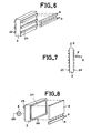
- FIG. 6 represents an alternative embodiment of the system of FIG. 4 which makes it possible to dispense with the optical device 3.
- a strip of DTC or photodiodes of length equal to that of a line of the sensitive screen 2 is used as the light sensor.
- the space between the transparent electrode 24 of the screen and the strip 4 is minimized so as to avoid optical losses.
- the screen is moved step by step after each line reading relative to the sensor 4.
- FIG. 7 representing a side view of the system of the figure making it possible to highlight the movement according to arrow D of the screen 2 in front of the sensor 4. It is quite obvious that according to another embodiment, it is possible to envisage moving the sensor 4 in front of the screen 2 then kept fixed.
- the optical device 3 of FIG. 5 is dispensed with.
- a matrix of photodiodes whose surface is equal to that of the sensitive screen 2.
- This matrix can be that which is obtained by production techniques on amorphous silicon.
- the array of photodiodes is pressed against the sensitive plate. The process then requires no mechanical movement.
- An output register 14 makes it possible to read the matrix of photodiodes and to transfer the results of reading on an output S to a processing circuit 8 not shown.
- a network of optical fibers 3 connect a line of the screen 2 to a sensor 4 made up of detectors arranged in a matrix. Such an embodiment is shown in FIG. 9.
- the ends 32 of the fibers are arranged in a line parallel to the axis X.
- the screen 2 is movable in a direction parallel to the axis Y so that all of the screen lines defined by the lines of electrodes 23, 24 is explored by the line of fiber ends 32.
- the sensor 4 comprises a matrix arrangement nxm of detectors. Each screen line then comprises nxm picture elements and the number of fibers 32 is also nxm. The ends of the fibers 33 are arranged in the form of a matrix of the same dimension as the matrix of detectors so that each end of the fiber 33 illuminates a detector of the sensor 4.
- the electrodes 23 are successively supplied with voltage by a generator 6 and an address circuit 16.
- the electrodes 24 are at fixed potential, earth for example.
- the sensor can in fact be a matrix of photosensitive charge transfer devices which are connected to the processing circuit not shown in FIG. 9.
- a line of light information corresponding to an image line is converted into a matrix of electrical signals which can be used by the processing circuit.
- a network of parallel fibers 30 and 31 are embedded in the phosphor material 20 of the screen.
- the screen 2 comprises, on either side of the phosphor material 20, electrodes parallel 23, 24 and orthogonal to the fibers 30, 31.
- the electrodes 23 are successively supplied with voltage by a generator 6 and an address circuit 16.
- the electrodes 24 are at a fixed potential, earth for example.
- the phosphor material included between this electrode and the electrode 24 located opposite, is excited and emits according to the energy previously accumulated, during exposure to X-rays, light energy, which as shown in Figure 11, is captured by each fiber.
- the light captured is trapped by each fiber, and by successive reflections is transmitted to a sensor 4 comprising detectors arranged in lines.
- the optical coupling between the screen 2 and the photon sensor 4, which is a photodetector strip is carried out using optical fibers which are integrated in the phosphor material 20.
- the electrical addressing is done for example by columns.
- the optical fibers are arranged along the lines, as shown in FIG. 10. So that the photons emitted during electrical stimulation are well captured by each fiber, it is possible to use an optical fiber converter of length d wave, that is to say which absorbs the photons emitted by the phosphor, at a wavelength ⁇ 1 then emits photons with a yield close to unity at a longer wavelength ⁇ 2.
- the process of absorption, re-emission and guidance is shown in Figure 11. This imaging process has the advantage of overcoming any mechanical movement during replay.
- FIG. 12 represents a variant of the embodiment of FIG. 2 in which the electrode 23 has been made blocking by providing a layer of a dielectric material 25 such as an organic material.
- the dielectric layer 25 is deposited on this metallic electrode. It is also possible, although this is not shown in the figures, to make the electrodes 24 blocking whether it is only the electrodes 24 or in addition to the electrodes 23. For this, a dielectric layer is provided between the phosphor material and the electrodes 24.
Landscapes
- High Energy & Nuclear Physics (AREA)
- Physics & Mathematics (AREA)
- Spectroscopy & Molecular Physics (AREA)
- General Physics & Mathematics (AREA)
- Life Sciences & Earth Sciences (AREA)
- Molecular Biology (AREA)
- Health & Medical Sciences (AREA)
- Engineering & Computer Science (AREA)
- General Engineering & Computer Science (AREA)
- Measurement Of Radiation (AREA)
- Analysing Materials By The Use Of Radiation (AREA)
- Radiography Using Non-Light Waves (AREA)
- Apparatus For Radiation Diagnosis (AREA)
- Facsimile Scanning Arrangements (AREA)
Applications Claiming Priority (2)
| Application Number | Priority Date | Filing Date | Title |
|---|---|---|---|
| FR8602876 | 1986-02-28 | ||
| FR8602876A FR2595145B1 (fr) | 1986-02-28 | 1986-02-28 | Systeme de visualisation a memoire |
Publications (1)
| Publication Number | Publication Date |
|---|---|
| EP0240384A1 true EP0240384A1 (de) | 1987-10-07 |
Family
ID=9332662
Family Applications (1)
| Application Number | Title | Priority Date | Filing Date |
|---|---|---|---|
| EP87400402A Withdrawn EP0240384A1 (de) | 1986-02-28 | 1987-02-24 | Bildsystem zur Speicherung |
Country Status (4)
| Country | Link |
|---|---|
| US (1) | US4818877A (de) |
| EP (1) | EP0240384A1 (de) |
| JP (1) | JPS62221337A (de) |
| FR (1) | FR2595145B1 (de) |
Cited By (1)
| Publication number | Priority date | Publication date | Assignee | Title |
|---|---|---|---|---|
| DE3910462A1 (de) * | 1988-04-01 | 1989-10-19 | Hitachi Ltd | Radiographische bildaufnahmevorrichtung |
Families Citing this family (9)
| Publication number | Priority date | Publication date | Assignee | Title |
|---|---|---|---|---|
| FR2634029A1 (fr) * | 1988-07-08 | 1990-01-12 | Thomson Csf | Equipement pour l'elaboration d'images radiologiques |
| DE4002432A1 (de) * | 1990-01-27 | 1991-08-01 | Philips Patentverwaltung | Verfahren zum messen von roentgen- oder gammastrahlung und dafuer geeignete messeinrichtung |
| US5142557A (en) * | 1990-12-21 | 1992-08-25 | Photometrics Ltd. | CCD and phosphor screen digital radiology apparatus and method for high resolution mammography |
| GB9326413D0 (en) * | 1993-12-24 | 1994-02-23 | British Nuclear Fuels Plc | Materials and devices incorporating phosphors |
| FR2727215B1 (fr) * | 1994-11-18 | 1996-12-20 | Thomson Csf | Dispositif de veille panoramique infrarouge statique a detecteurs matriciels multiples |
| NO304859B1 (no) * | 1997-06-06 | 1999-02-22 | Opticom As | Optisk logisk element og fremgangsmÕter til henholdsvis dets preparering og optiske adressering, samt anvendelse derav i en optisk logisk innretning |
| FR2750487B1 (fr) * | 1996-06-28 | 2005-10-21 | Thomson Csf | Revetement pour la protection personnelle d'un fantassin |
| DE60309955T2 (de) * | 2002-02-20 | 2007-09-20 | Fujifilm Corp. | Verfahren und Vorrichtung zur Reproduktion eines Strahlungsbildes |
| JP4933258B2 (ja) * | 2003-09-22 | 2012-05-16 | クイデル コーポレーション | 試料中の複数分析物の検出装置 |
Citations (5)
| Publication number | Priority date | Publication date | Assignee | Title |
|---|---|---|---|---|
| GB1185832A (en) * | 1966-06-03 | 1970-03-25 | Thorn Electrical Ind Ltd | Improvements in and relating to Electroluminescent Devices |
| GB1466869A (en) * | 1974-08-02 | 1977-03-09 | Secr Defence | Light storage systems |
| EP0007105A1 (de) * | 1978-07-12 | 1980-01-23 | Fuji Photo Film Co., Ltd. | Verfahren und Vorrichtung zum Auslesen eines in einer phosphoreszierenden Substanz registrierten Strahlungsbildes |
| US4210805A (en) * | 1977-02-17 | 1980-07-01 | Tokyo Shibaura Electric Co., Ltd. | Semiconductor radiation detector |
| EP0156258A2 (de) * | 1984-03-15 | 1985-10-02 | Fuji Photo Film Co., Ltd. | Lichtleiterbauteil zum Auslesen von Strahlungsbildern |
Family Cites Families (23)
| Publication number | Priority date | Publication date | Assignee | Title |
|---|---|---|---|---|
| US3500101A (en) * | 1955-02-02 | 1970-03-10 | Sylvania Electric Prod | Photocapacitive electroluminescent light amplifier |
| US2990473A (en) * | 1955-05-04 | 1961-06-27 | Research Corp | Method for recording, detecting and measuring radiation and for recording and recalling data |
| US2933602A (en) * | 1955-10-10 | 1960-04-19 | Du Pont | Apparatus for generating visible light by photo-electroluminescence |
| GB1208308A (en) * | 1966-10-27 | 1970-10-14 | Matsushita Electric Ind Co Ltd | Electroluminescent display devices |
| GB1251226A (de) * | 1967-11-20 | 1971-10-27 | ||
| US3710127A (en) * | 1971-04-19 | 1973-01-09 | Matsushita Electric Ind Co Ltd | Solid-state image converter having composite energy sensing element |
| FR2233645B1 (de) * | 1973-05-29 | 1976-04-23 | Thomson Csf | |
| FR2241846B1 (de) * | 1973-08-21 | 1977-09-09 | Thomson Csf | |
| US3932756A (en) * | 1974-06-24 | 1976-01-13 | Sybron Corporation | X-ray detector for a panoramic X-ray device |
| FR2305743A1 (fr) * | 1975-03-25 | 1976-10-22 | Thomson Csf | Dispositif de detection de rayons x |
| FR2311328A1 (fr) * | 1975-05-16 | 1976-12-10 | Thomson Csf | Dispositif de commande optique de photosensibilite d'un milieu cristallin et systeme de stockage optique comportant un tel dispositif |
| FR2312052A1 (fr) * | 1975-05-23 | 1976-12-17 | Thomson Csf | Dispositif optique de stockage holographique et systeme de stockage tridimensionnel utilisant un tel dispositif |
| FR2318484A1 (fr) * | 1975-07-17 | 1977-02-11 | Thomson Csf | Dispositif optique de stockage et d'effacement selectif de donnees et memoire optique comportant un tel dispositif |
| FR2376549A1 (fr) * | 1977-01-04 | 1978-07-28 | Thomson Csf | Systeme bistable a electrets |
| FR2376477A1 (fr) * | 1977-01-04 | 1978-07-28 | Thomson Csf | Cellule d'affichage electrostatique et dispositif d'affichage comprenant une telle cellule |
| FR2376548A1 (fr) * | 1977-01-04 | 1978-07-28 | Thomson Csf | Dispositif bistable electrostatique |
| FR2399039A1 (fr) * | 1977-07-29 | 1979-02-23 | Thomson Csf | Dispositif de detection de rayonnement ionisant, et dispositif de tomodensitometrie comportant un tel dispositif |
| FR2404271A1 (fr) * | 1977-09-23 | 1979-04-20 | Thomson Csf | Dispositif de visualisation comportant une couche mince de cristal liquide accolee a une lame photoconductrice |
| JPS5917400B2 (ja) * | 1979-07-11 | 1984-04-20 | 富士写真フイルム株式会社 | 放射線像変換パネル |
| US4492121A (en) * | 1982-09-30 | 1985-01-08 | The United States Of America As Represented By The Secretary Of The Navy | Gauge for measuring high transient pressures |
| JPH06105261B2 (ja) * | 1984-03-05 | 1994-12-21 | 株式会社東芝 | 濃度勾配測定装置 |
| FR2583579B1 (fr) * | 1985-06-14 | 1987-08-07 | Thomson Csf | Procede d'obtention d'un materiau piezoelectrique et dispositif de mise en oeuvre |
| FR2583914B1 (fr) * | 1985-06-21 | 1989-04-07 | Thomson Csf | Materiaux dielectriques a base de polymeres et a permittivite dielectrique elevee |
-
1986
- 1986-02-28 FR FR8602876A patent/FR2595145B1/fr not_active Expired
-
1987
- 1987-02-24 EP EP87400402A patent/EP0240384A1/de not_active Withdrawn
- 1987-02-25 US US07/018,532 patent/US4818877A/en not_active Expired - Fee Related
- 1987-02-27 JP JP62045070A patent/JPS62221337A/ja active Pending
Patent Citations (5)
| Publication number | Priority date | Publication date | Assignee | Title |
|---|---|---|---|---|
| GB1185832A (en) * | 1966-06-03 | 1970-03-25 | Thorn Electrical Ind Ltd | Improvements in and relating to Electroluminescent Devices |
| GB1466869A (en) * | 1974-08-02 | 1977-03-09 | Secr Defence | Light storage systems |
| US4210805A (en) * | 1977-02-17 | 1980-07-01 | Tokyo Shibaura Electric Co., Ltd. | Semiconductor radiation detector |
| EP0007105A1 (de) * | 1978-07-12 | 1980-01-23 | Fuji Photo Film Co., Ltd. | Verfahren und Vorrichtung zum Auslesen eines in einer phosphoreszierenden Substanz registrierten Strahlungsbildes |
| EP0156258A2 (de) * | 1984-03-15 | 1985-10-02 | Fuji Photo Film Co., Ltd. | Lichtleiterbauteil zum Auslesen von Strahlungsbildern |
Cited By (1)
| Publication number | Priority date | Publication date | Assignee | Title |
|---|---|---|---|---|
| DE3910462A1 (de) * | 1988-04-01 | 1989-10-19 | Hitachi Ltd | Radiographische bildaufnahmevorrichtung |
Also Published As
| Publication number | Publication date |
|---|---|
| US4818877A (en) | 1989-04-04 |
| FR2595145B1 (fr) | 1989-03-31 |
| JPS62221337A (ja) | 1987-09-29 |
| FR2595145A1 (fr) | 1987-09-04 |
Similar Documents
| Publication | Publication Date | Title |
|---|---|---|
| US5594253A (en) | Hybrid luminescent device for imaging of ionizing and penetrating radiation | |
| US6452184B1 (en) | Microchannel high resolution x-ray sensor having an integrated photomultiplier | |
| JP3445164B2 (ja) | 静電記録体、静電潜像記録装置および静電潜像読取装置 | |
| EP1356267B1 (de) | Verfahren und vorrichtungen zur lichtanregung und sammlung für speicherleuchtstoff-bildplatten | |
| TWI470262B (zh) | 形成於閃爍器上之放射線偵測器 | |
| US5196702A (en) | Photo-sensor and method for operating the same | |
| US4554453A (en) | Apparatus for recording X-ray images | |
| JPS60111568A (ja) | 放射線画像情報読取装置 | |
| US7087915B2 (en) | Radiation image reproducing device and method for reproducing radiation image | |
| JPWO2003083513A1 (ja) | X線検出器 | |
| US4983834A (en) | Large area particle detector system | |
| CA2228325C (en) | X-ray image intensifier | |
| EP0240384A1 (de) | Bildsystem zur Speicherung | |
| JPH11271457A (ja) | X線イメ―ジング・システム | |
| CN113169014A (zh) | 用于检测x射线的高分辨率光阀检测器 | |
| FR2621705A1 (fr) | Detecteur multiradiations, notamment detecteur de rayons x a double energie | |
| JP2007127734A (ja) | 放射線画像情報検出パネルおよび放射線画像情報読取装置 | |
| JP2004317300A (ja) | 放射線平面検出器及びその製造方法 | |
| EP0983521B1 (de) | Abbildender festkörperdetektor der einer ionisierenden strahlung ausgestzt ist und ein messgerät aufweist | |
| FR2698184A1 (fr) | Procédé et dispositif capteur d'images par rayons X utilisant la post-luminiscence d'un scintillateur. | |
| US6504166B2 (en) | Method and apparatus for recording image in recording medium using photoconductor with reduced dark latent image, and reading image from photoconductor with reduced dark current | |
| CN105378507B (zh) | 辐射检测器、闪烁体板和制造它们的方法 | |
| FR2519179A1 (fr) | Convertisseur d'image radiologique | |
| Risticj | The digital flat-panel x-ray detectors | |
| FR2803394A1 (fr) | Systeme de detection d'image radiologique pour generateur de rayons x a balayage |
Legal Events
| Date | Code | Title | Description |
|---|---|---|---|
| PUAI | Public reference made under article 153(3) epc to a published international application that has entered the european phase |
Free format text: ORIGINAL CODE: 0009012 |
|
| AK | Designated contracting states |
Kind code of ref document: A1 Designated state(s): DE GB IT NL |
|
| 17P | Request for examination filed |
Effective date: 19871104 |
|
| RAP3 | Party data changed (applicant data changed or rights of an application transferred) |
Owner name: THOMSON-CSF |
|
| 17Q | First examination report despatched |
Effective date: 19890424 |
|
| STAA | Information on the status of an ep patent application or granted ep patent |
Free format text: STATUS: THE APPLICATION IS DEEMED TO BE WITHDRAWN |
|
| 18D | Application deemed to be withdrawn |
Effective date: 19890829 |
|
| RIN1 | Information on inventor provided before grant (corrected) |
Inventor name: MICHERON, FRANCOIS Inventor name: MAILLOT, CHRISTIAN Inventor name: AYRAL, JEAN-LUC |