EP0240245B1 - Erkennen von Gleichstrom bei Vorhandensein von Datensignalen - Google Patents
Erkennen von Gleichstrom bei Vorhandensein von Datensignalen Download PDFInfo
- Publication number
- EP0240245B1 EP0240245B1 EP87302623A EP87302623A EP0240245B1 EP 0240245 B1 EP0240245 B1 EP 0240245B1 EP 87302623 A EP87302623 A EP 87302623A EP 87302623 A EP87302623 A EP 87302623A EP 0240245 B1 EP0240245 B1 EP 0240245B1
- Authority
- EP
- European Patent Office
- Prior art keywords
- signal
- occurrence
- filter
- collision
- component
- Prior art date
- Legal status (The legal status is an assumption and is not a legal conclusion. Google has not performed a legal analysis and makes no representation as to the accuracy of the status listed.)
- Expired - Lifetime
Links
- 238000001514 detection method Methods 0.000 title claims abstract description 29
- 238000000034 method Methods 0.000 claims abstract description 8
- 238000001914 filtration Methods 0.000 claims description 5
- 230000003111 delayed effect Effects 0.000 claims 1
- 238000009966 trimming Methods 0.000 abstract description 3
- 238000010586 diagram Methods 0.000 description 4
- 239000003990 capacitor Substances 0.000 description 2
- 230000000295 complement effect Effects 0.000 description 2
- 238000010276 construction Methods 0.000 description 2
- 230000001934 delay Effects 0.000 description 2
- 238000004519 manufacturing process Methods 0.000 description 2
- 239000000654 additive Substances 0.000 description 1
- 230000000996 additive effect Effects 0.000 description 1
- 230000002238 attenuated effect Effects 0.000 description 1
- 230000005540 biological transmission Effects 0.000 description 1
- 125000004122 cyclic group Chemical group 0.000 description 1
- 230000008030 elimination Effects 0.000 description 1
- 238000003379 elimination reaction Methods 0.000 description 1
- 230000003993 interaction Effects 0.000 description 1
- 230000001052 transient effect Effects 0.000 description 1
Images
Classifications
-
- H—ELECTRICITY
- H04—ELECTRIC COMMUNICATION TECHNIQUE
- H04L—TRANSMISSION OF DIGITAL INFORMATION, e.g. TELEGRAPHIC COMMUNICATION
- H04L12/00—Data switching networks
- H04L12/28—Data switching networks characterised by path configuration, e.g. LAN [Local Area Networks] or WAN [Wide Area Networks]
- H04L12/40—Bus networks
- H04L12/40006—Architecture of a communication node
- H04L12/40032—Details regarding a bus interface enhancer
-
- H—ELECTRICITY
- H04—ELECTRIC COMMUNICATION TECHNIQUE
- H04L—TRANSMISSION OF DIGITAL INFORMATION, e.g. TELEGRAPHIC COMMUNICATION
- H04L12/00—Data switching networks
- H04L12/28—Data switching networks characterised by path configuration, e.g. LAN [Local Area Networks] or WAN [Wide Area Networks]
- H04L12/40—Bus networks
- H04L12/407—Bus networks with decentralised control
- H04L12/413—Bus networks with decentralised control with random access, e.g. carrier-sense multiple-access with collision detection [CSMA-CD]
Definitions
- This invention relates to high-frequency data transmission over a network and, more particularly, to a method and apparatus for the detection of a direct current voltage in the presence of a high frequency data stream so as to avoid "collisions", i.e., the presence of more than one station attempting to transmit data simultaneously on the network.
- a set of standards have been promulgated by the Institute of Electrical and Electronic Engineers (IEEE) which specify the port characteristics for a coaxial media interface to Data Terminal Equipment (DTE).
- IEEE 802.3 Local Area Network Standard employs a "collision detection" method to indicate the presence of more than one station attempting to transmit data simultaneously on the network.
- the transmitted data "packet” is composed of both alternating current (AC) and direct current (DC) components.
- AC alternating current
- DC direct current
- the IEEE 802.3 standard makes certain recommendations for the "no detect” and “must detect” levels on the network. They are based on calculations made for both 10 Base 5 - Ethernet and 10 Base 2 - Cheapernet specifications, namely a 5 ohm DC loop resistance and a 10 ohm DC loop system, respectively. For longer networks the DC loop resistances are larger than these values and the collision detect window shrinks until it is impossible to distinguish the two conditions. These considerations lead to a 150 millivolt (mV) to 200 mV collision detect window.
- mV millivolt
- the IEEE 802.3 standard requires that a collision indication should occur within nine bit times of the actual collision on the coaxial medium. For a 10 megabit per second (Mbps) data stream this is 900 nanoseconds (ns). For a collision detection circuit, which will include a low-pass filter and logic gates, the total delay in the collision detect path must not exceed 900 ns, which places a premium on limiting low-pass filter response and gate delays.
- the AC component of the signal in which the collision detection circuit must operate is approximately 2 volts peak-to-peak at 10 Mbps.
- a collision detection method which is suitable for implementation is an integrated circuit package, is described which eliminates the need for field adjustments.
- the apparatus implementing the collision detection method works over a wide temperature range and the manufacturing process employed in integrated circuits permits rigid control over the individual component parameters.
- the method involves comparison of the signal received over the network with a collision reference voltage V COL .
- the resulting difference signal is passed through a three-pole cyclical (synchronously-tuned) low-pass filter.
- the output signal from the filter is coupled to a high-gain comparator which acts as a zero-crossing detector.
- the comparator generates ECL logic signals representing occurrence and non-occurrence of a collision.
- These signals are conducted to two time-delay generators, performing 100 ns and 200 ns delays, respectively, and their output signals provide the set and reset input signals, respectively, to an S-R latch.
- the delay generators act as pulse-width discriminators for LOW-going pulses.
- the latch in conjuction with the delay generators, prevents toggling between the collision and no-collision states, in the presence of large transient signals which may occur at the near-end of the network.
- the time-delay generators eliminate any uncertainty in the detection of collisions due to the residual ripple after the signal has passed through the three-pole low-pass filter.
- the low-pass filter is a three-pole cascaded cyclic (synchronously-tuned) RC filter which is simple to realize and has poles at the same location on the real axis. Consequently, it does not have any overshoot in its step response and thereby avoids false detection of collisions. It also provides the minimum delay for a real-pole implementation.
- Elimination of inductances in the low-pass filter allows the collision detection apparatus to be implemented as part of an integrated circuit. Since the filter employs three fully-isolated stages, there is no filter section interaction.
- the collision detection apparatus operates in a differential mode and is DC-balanced at the voltage of interest, namely the collision reference voltage V COL . As a result, the collision detection apparatus is independent of filter stage gain.
- the present invention provides a method for detection of a direct current (dc) component exceeding a predetermined voltage on a single-ended signal line ["collision”] also having an alternating current (ac) component, characterised by the steps:
- the present invention also provides an integrated circuit device for detecting a direct current (dc) component exceeding a predetermined voltage on a single-ended signal line ["a collision"] also having an alternating current (ac) component, characterised in that said device includes means 18 for generating a signal representing the difference between the signal on said signal line and said predetermined voltage, a low-pass filter 20 receiving said difference signal and removing said ac component therefrom comprising: a differential input stage for receiving said difference signal; a plurality of single-ended filter stages, a first of which is responsive to the signal generated by said first input stage, each constituting an RC-filter section, each responsive to the RC-filter signal generated by its predecessor; a final differential output stage, responsive to the RC-filtered signal generated by the last of said plurality of single-ended filter stages, and comparator means for comparing said filter signal with a zero level and generating signals indicating the occurrence or non-occurrence of a satisfactory comparison if said filter signal is below or above said zero level respectively.
- dc direct
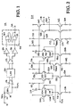
- Fig. 1 is a block diagram of the collision detection device of the instant invention.
- Fig. 2 is a schematic diagram of the low-pass filter employed within the collision detection device.
- a collision detection device 10 of the instant invention is illustrated in block diagram form.
- the signal received from the network over "tap" 12 is conducted via a 4:1 attenuation network consisting of a 75 kil ohm (Kohm) resistor 14 and a 25 Kohm resistor 16.
- the attenuated signal across resistor 16 is applied to the input terminals of a differential operational amplifier 18.
- the negative terminal of operational amplifier 18 also receives a collision reference voltage (V COL ).
- the resulting difference signal generated at the differential output terminals of operatinal amplifier 18 are conducted to a low-pass filter (LPF) 20.
- LPF low-pass filter
- Filter 20 attenuates the ac component of the difference signal to approximately 20 mV for a 2 volt ac component appearing at the tap 12.
- the design of the low-pass filter 20 will be described hereinbelow in connection with Fig. 2.
- the filtered signals generated by LPF 20 are conducted to a comparator 22 which operates as a zero-crossing detector.
- Comparator 22 generates emitter-coupled logic (ECL) signals at a true and at a complement output terminal.
- ECL emitter-coupled logic
- the signal at the true output terminal of comparator 22 is conducted to a 100 nsec delay generator 24.
- the signal at the complemented output terminal of comparator 22 is conducted to a 200 nsec delay generator 26.
- These delay generators generate signals conducted to a set-reset (S-R) latch 28 comprising a pair of NOR gates 30 and 32.
- S-R latch 28 at a terminal 34 is indicative of the detection of a collision.
- the 100 nsec delay generator 24 detects a LOW pulse-width during the preamble portion of a data packet; a 5 MHz signal having a 50% duty cycle produces a LOW-going pulse of 100 nsec duration. This detection causes S-R latch 28 to be set.
- the LPF 20 is of a three-pole cyclical, or synchronously-tuned, design. It employs RC filtering and is particularly suited for inclusion in an integrated-circuit package since it does not employ inductors as do the prior art discrete circuit devices, and because of the manufacturing process used for integrated circuits, the component values may be closely controlled so that trimming is unnecessary.
- the LPF 20 has each of its poles at 1.8 MHz to filter 5 MHz ac components.
- the delay generators 24 and 26 are preferably of a type suitable for use in integrated circuits.
- One such time-delay device is described in a copending patent application "An Interruptable Voltage-Controlled Oscillator" filed August 5, 1983 on behalf of Dave Campbell, U.S. Ser. No. 520,876.
- Fig. 2 is a schematic diagram of the LPF 20 employed in the collison detection device 10 of the instant invention.
- Three separate single-ended stages are employed within LPF 20, rather than differential stages so as to minimize the number of components required by the LPF. Furthermore, differential stages could potentially saturate if employed in the collision detection device 10 and accordingly would not conduct signals properly.
- a last, fourth, stage of LPF 20 produces a buffered pseudo-differential signal at the output terminals of LPF 20 for use by the remaining elements 22, 24, 26 and 28 of the collision detector of Fig. 1.
- the signals generated by differential operational amplifier 18 are received at terminals 100 and 102 of LPF 20 and conducted to the base of NPN transistors 104 and 106, respectively, of the first stage of LPF 20.
- the collector of transistor 104 is connected to a source of positive voltage and its emitter is connected to a first lead of a resistor 108.
- the collector of transistor 106 is ac-coupled to the source of positive voltage via a capacitor 110 and dc-coupled via a resistor 112.
- the emitter of transistor 106 is connected to a first lead of a resistor 114.
- the second leads of resistors 108 and 114 are connected in common and to the collector of an NPN transistor 116.
- the emitter of transistor 116 is coupled to ground via a resistor 118 and its base is connected to a source of bias voltage V CS .
- the second stage of LPF 20 is of similar construction to that of the first stage and will accordingly not be described in detail except to note that it receives the signal generated by the first stage at the base of a transistor 120 (corresponding to transistor 104 in the first stage) connected to the collector of transistor 106, and that the base of the transistor 122 (corresponding to transistor 106) is connected to a source of bias voltage comprising a series connection of a resistor 136, NPN transistors 138 and 140, and a resistor 142, a first lead of resistor 136 connected to the positive voltage source and a second lead of resistor 142 connected to ground.
- the base of transistor 138 is connected to a source of bias voltage V BB2 and the base of transistor 140 to the source of bias voltage V CS .
- the second stage of LPF 20 is operated in a single-ended mode.
- a third stage of LPF 20 identical in construction to that of the second stage sharing the source of bias voltage comprising elements 136, 138, 140 and 142 receives the signal generated by the second stage and generates therefrom a signal conducted to the fourth stage of LPF20.
- the fourth stage includes an NPN transistor 160 receiving at its base the signal generated by the third stage.
- the collector of transistor 160 is connected to the source of positive voltage and its emitter is connected to ground via an NPN transistor 162 and resistor 164.
- the base of transistor 162 is connected to the source of bias voltage V CS .
- the signal at the emitter of transistor 160 is one of the pair of signals generated by LPF 20 and conducted to comparator 22.
- the second of this pair of signals is generated at the emitter of an NPN transistor 166 which has its collector connected to the source of positive voltage, its base connected via a resistor 168 to a source of bias voltage comprising a series connection of a resistor 170, NPN transistors 172 and 174, and a resistor 176, connected to the positive voltage source, the source of bias voltages V BB2 and V CS , and ground, similarly to that of the bias voltage source shared by stages two and three of the LPF 20.
- the signal generated at the emitters of transistors 160 and 166 and conducted to terminals 178 and 180 is thus a balanced matched differential output signal.
- the LPF 20 attentuates the ac component of the nominal signal applied at the tap 12 to approximately 20 mV, while producing a signal at terminals 178 and 180 indicative of the presence or absence of a dc component in the signal applied at tap 12 exceeding the collision reference voltage V COL .
- To achieve this attenuation with a single-pole filter would require an RC-filter constant of 820 nsec resulting in a 10% to 90% step response of 1800 nsec and would greatly exceed the 900 nsec delay specified by the IEEE 802.3 standard.
- the LPF 20 does not overshoot in its step response because of its implementation with real poles. As a result, detection of "false" collisions is eliminated.
Landscapes
- Engineering & Computer Science (AREA)
- Computer Networks & Wireless Communication (AREA)
- Signal Processing (AREA)
- Small-Scale Networks (AREA)
- Lubrication Of Internal Combustion Engines (AREA)
- Control Of Motors That Do Not Use Commutators (AREA)
- Electrical Discharge Machining, Electrochemical Machining, And Combined Machining (AREA)
- Measurement And Recording Of Electrical Phenomena And Electrical Characteristics Of The Living Body (AREA)
- Investigating Or Analyzing Materials By The Use Of Magnetic Means (AREA)
- Manipulation Of Pulses (AREA)
Claims (5)
- Verfahren zum Erkennen einer eine vorbestimmte Spannung übersteigenden Gleichstromkomponente (dc) auf einer einpoligen Signalleitung (12), die ferner eine Wechselstromkomponente (ac) aufweist, gekennzeichnet durch die folgenden Schritte:a) Erzeugen (18) eines Signals, das die Differenz zwischen dem Signal auf der Signalleitung und der vorbestimmten Spannung angibt,b) Filtern (20) der Wechselstromkomponente aus dem Differenzsignal; undc) Vergleichen (22) des gefilterten Signals mit einem Null-Pegel und Erzeugen von Signalen, die das Vorhandensein oder das Nichtvorhandensein eines zufriedenstellenden Vergleichs angeben, wenn das gefilterte Signal unter bzw. über dem Null-Pegel liegt.
- Kollisionserkennungsverfahren nach Anspruch 1, ferner gekennzeichnet durch die folgenden Schritte:d) Verzögern der das Vorhandensein oder das Nichtvorhandensein anzeigenden Signale um einen ersten bzw. einen zweiten vorbestimmten Betrag, wodurch eine Impulsbreitenunterscheidung der im Schritt (a) erzeugten Signale bewirkt wird; unde) Anlegen des um den ersten bzw. den zweiten vorbestimmten Betrag verzögerten Signals an einen Setz- bzw. einen Rücksetzeingang eines S-R-Haltespeichers, wobei der Zustand des S-R-Haltespeichers das Erkennen oder das Nicht-Erkennen der die vorbestimmte Spannung übersteigenden Gleichstromkomponente angibt.
- Kollisionserkennungsverfahren nach Anspruch 1, dadurch gekennzeichnet, daß der Schritt (b) des Filterns das Filtern des Differenzsignals durch eine Reihe von RC-Filtern beinhaltet.
- Integrierte Schaltungsvorrichtung (10) zum Erkennen einer eine vorbestimmte Spannung übersteigenden Gleichstromkomponente auf einer einpoligen Signalleitung (12), die ferner eine Wechselstromkomponente (ac) aufweist,
dadurch gekennzeichnet, daß die Vorrichtung eine Einrichtung (18) zum Erzeugen eines Signals, das die Differenz zwischen dem Signal auf der Signalleitung und der vorbestimmten Spannung angibt, und ein Tiefpaßfilter (20) aufweist, das das Differenzsignal empfängt und die Wechselstromkomponente aus diesem entfernt und aufweist:- eine Differenzeingangsstufe zum Empfangen des Differenzsignals;- mehrere einpolige Filterstufen (104, 106, 116; 120, 122, 132; 144, 146, 156), von denen eine erste auf das von der ersten Eingangsstufe erzeugte Signal reagiert, wobei jede einen RC-Filterabschnitt bildet, von denen jeder auf das von dem Vorgänger erzeugte RC-Filtersignal reagiert;- eine Differenz-Endausgangsstufe (160, 162, 166), die auf das von der letzten der mehreren einpoligen Filterstufen erzeugte RC-gefilterte Signal reagiert, und eine Komparatoreinrichtung (22) zum Vergleichen des Filtersignals mit einem Null-Pegel und zum Erzeugen von Signalen, die, wenn das Filtersignal unter oder über dem Null-Pegel liegt, das Vorhandensein oder das Nichtvorhandensein eines zufriedenstellenden Vergleichs angeben. - Integrierte Schaltungsvorrichtung nach Anspruch 4, dadurch gekennzeichnet, daß sich der RC-Pol jeder der mehreren einpoligen RC-Filterstufen des Tiefpaßfilters auf derselben Position auf der realen Achse in der S-Ebene befindet.
Applications Claiming Priority (2)
| Application Number | Priority Date | Filing Date | Title |
|---|---|---|---|
| US847805 | 1986-04-03 | ||
| US06/847,805 US4734596A (en) | 1986-04-03 | 1986-04-03 | Detection of direct current in the presence of manchester-encoded signals |
Publications (3)
| Publication Number | Publication Date |
|---|---|
| EP0240245A2 EP0240245A2 (de) | 1987-10-07 |
| EP0240245A3 EP0240245A3 (en) | 1989-09-20 |
| EP0240245B1 true EP0240245B1 (de) | 1994-10-12 |
Family
ID=25301559
Family Applications (1)
| Application Number | Title | Priority Date | Filing Date |
|---|---|---|---|
| EP87302623A Expired - Lifetime EP0240245B1 (de) | 1986-04-03 | 1987-03-26 | Erkennen von Gleichstrom bei Vorhandensein von Datensignalen |
Country Status (5)
| Country | Link |
|---|---|
| US (1) | US4734596A (de) |
| EP (1) | EP0240245B1 (de) |
| JP (1) | JP2607879B2 (de) |
| AT (1) | ATE112910T1 (de) |
| DE (1) | DE3750644T2 (de) |
Families Citing this family (4)
| Publication number | Priority date | Publication date | Assignee | Title |
|---|---|---|---|---|
| JPH03172014A (ja) * | 1989-11-30 | 1991-07-25 | Toshiba Corp | アクティブ・フィルタ |
| US5107491A (en) * | 1990-02-20 | 1992-04-21 | Advanced Micro Devices, Inc. | Collision filter |
| JPH05335937A (ja) * | 1992-05-28 | 1993-12-17 | Mitsubishi Electric Corp | 周波数分周回路 |
| US5267237A (en) * | 1992-07-07 | 1993-11-30 | Digital Equipment Corporation | Collison detection and signaling circuit |
Family Cites Families (4)
| Publication number | Priority date | Publication date | Assignee | Title |
|---|---|---|---|---|
| US4308502A (en) * | 1980-03-31 | 1981-12-29 | Bell Telephone Laboratories, Incorporated | Threshold detection |
| US4412347A (en) * | 1981-05-26 | 1983-10-25 | Digital Equipment Corporation | Precision setting of currents and reference voltages |
| JPS5848209A (ja) * | 1981-09-14 | 1983-03-22 | Sony Corp | 情報信号有無判別回路装置 |
| US4524291A (en) * | 1983-01-06 | 1985-06-18 | Motorola, Inc. | Transition detector circuit |
-
1986
- 1986-04-03 US US06/847,805 patent/US4734596A/en not_active Expired - Lifetime
-
1987
- 1987-03-26 DE DE3750644T patent/DE3750644T2/de not_active Expired - Lifetime
- 1987-03-26 AT AT87302623T patent/ATE112910T1/de not_active IP Right Cessation
- 1987-03-26 EP EP87302623A patent/EP0240245B1/de not_active Expired - Lifetime
- 1987-04-01 JP JP62082192A patent/JP2607879B2/ja not_active Expired - Lifetime
Also Published As
| Publication number | Publication date |
|---|---|
| DE3750644T2 (de) | 1995-05-11 |
| EP0240245A3 (en) | 1989-09-20 |
| US4734596A (en) | 1988-03-29 |
| JPS63119340A (ja) | 1988-05-24 |
| EP0240245A2 (de) | 1987-10-07 |
| ATE112910T1 (de) | 1994-10-15 |
| DE3750644D1 (de) | 1994-11-17 |
| JP2607879B2 (ja) | 1997-05-07 |
Similar Documents
| Publication | Publication Date | Title |
|---|---|---|
| US5828476A (en) | Dual rate, burst mode, radiation hardened, optical transceiver | |
| US5903605A (en) | Jitter detection method and apparatus | |
| US6438178B1 (en) | Integrated circuit for receiving a data stream | |
| US5327465A (en) | Method and apparatus for squelch circuit in network communication | |
| US4656661A (en) | Switched capacitor coupled line receiver circuit | |
| US6246718B1 (en) | Method and apparatus for decoding a bit sequence for transmission over pots wiring | |
| US6272185B1 (en) | Method and apparatus for performing data pulse detection | |
| US5812597A (en) | Circuit for preventing base line wander of digital signals in a network receiver | |
| US6148025A (en) | System and method for compensating for baseline wander | |
| JPH10304004A (ja) | 改良した物理層インターフェース装置 | |
| JPS61502510A (ja) | アダプティブ・ハイブリッド回路 | |
| JPH02277338A (ja) | ローカルエリアネットワークの放送局ロケータ | |
| DE69921092T2 (de) | Signalisierung unter verwendung eines impedanzsmodulators | |
| US5132926A (en) | Token ring equalizer | |
| US4412347A (en) | Precision setting of currents and reference voltages | |
| US4380088A (en) | Tester for collision-detect circuitry | |
| US8310310B2 (en) | Burst mode amplifier | |
| US5555277A (en) | Technique for cancelling common mode switching noise to achieve reduced error rates in a local area network | |
| US4734596A (en) | Detection of direct current in the presence of manchester-encoded signals | |
| US5898729A (en) | Fault tolerant digital transmission system | |
| EP0303410B1 (de) | Nichtlineare Squelch-Schaltung | |
| US6060890A (en) | Apparatus and method for measuring the length of a transmission cable | |
| EP0606413B1 (de) | Verfahren und mittel für automatische detektion und korrektur eines polaritätsfehlers in einem aus verdrillten paaren bestehenden medium | |
| EP1145426B1 (de) | Datenimpulsempfänger | |
| US5418821A (en) | Method and apparatus for sample-data receiver squelch |
Legal Events
| Date | Code | Title | Description |
|---|---|---|---|
| PUAI | Public reference made under article 153(3) epc to a published international application that has entered the european phase |
Free format text: ORIGINAL CODE: 0009012 |
|
| AK | Designated contracting states |
Kind code of ref document: A2 Designated state(s): AT BE CH DE ES FR GB GR IT LI LU NL SE |
|
| PUAL | Search report despatched |
Free format text: ORIGINAL CODE: 0009013 |
|
| AK | Designated contracting states |
Kind code of ref document: A3 Designated state(s): AT BE CH DE ES FR GB GR IT LI LU NL SE |
|
| 17P | Request for examination filed |
Effective date: 19891215 |
|
| 17Q | First examination report despatched |
Effective date: 19911104 |
|
| GRAA | (expected) grant |
Free format text: ORIGINAL CODE: 0009210 |
|
| AK | Designated contracting states |
Kind code of ref document: B1 Designated state(s): AT BE CH DE ES FR GB GR IT LI LU NL SE |
|
| PG25 | Lapsed in a contracting state [announced via postgrant information from national office to epo] |
Ref country code: GR Free format text: LAPSE BECAUSE OF FAILURE TO SUBMIT A TRANSLATION OF THE DESCRIPTION OR TO PAY THE FEE WITHIN THE PRESCRIBED TIME-LIMIT Effective date: 19941012 |
|
| REF | Corresponds to: |
Ref document number: 112910 Country of ref document: AT Date of ref document: 19941015 Kind code of ref document: T |
|
| REF | Corresponds to: |
Ref document number: 3750644 Country of ref document: DE Date of ref document: 19941117 |
|
| ITF | It: translation for a ep patent filed | ||
| ET | Fr: translation filed | ||
| PG25 | Lapsed in a contracting state [announced via postgrant information from national office to epo] |
Ref country code: ES Free format text: LAPSE BECAUSE OF FAILURE TO SUBMIT A TRANSLATION OF THE DESCRIPTION OR TO PAY THE FEE WITHIN THE PRESCRIBED TIME-LIMIT Effective date: 19950123 |
|
| EAL | Se: european patent in force in sweden |
Ref document number: 87302623.1 |
|
| PLBE | No opposition filed within time limit |
Free format text: ORIGINAL CODE: 0009261 |
|
| STAA | Information on the status of an ep patent application or granted ep patent |
Free format text: STATUS: NO OPPOSITION FILED WITHIN TIME LIMIT |
|
| 26N | No opposition filed | ||
| PGFP | Annual fee paid to national office [announced via postgrant information from national office to epo] |
Ref country code: LU Payment date: 19980123 Year of fee payment: 12 |
|
| PGFP | Annual fee paid to national office [announced via postgrant information from national office to epo] |
Ref country code: AT Payment date: 19980206 Year of fee payment: 12 |
|
| PGFP | Annual fee paid to national office [announced via postgrant information from national office to epo] |
Ref country code: SE Payment date: 19980302 Year of fee payment: 12 |
|
| PGFP | Annual fee paid to national office [announced via postgrant information from national office to epo] |
Ref country code: CH Payment date: 19980415 Year of fee payment: 12 |
|
| PGFP | Annual fee paid to national office [announced via postgrant information from national office to epo] |
Ref country code: BE Payment date: 19980416 Year of fee payment: 12 |
|
| PG25 | Lapsed in a contracting state [announced via postgrant information from national office to epo] |
Ref country code: LU Free format text: LAPSE BECAUSE OF NON-PAYMENT OF DUE FEES Effective date: 19990326 Ref country code: AT Free format text: LAPSE BECAUSE OF NON-PAYMENT OF DUE FEES Effective date: 19990326 |
|
| PG25 | Lapsed in a contracting state [announced via postgrant information from national office to epo] |
Ref country code: SE Free format text: LAPSE BECAUSE OF NON-PAYMENT OF DUE FEES Effective date: 19990327 |
|
| PG25 | Lapsed in a contracting state [announced via postgrant information from national office to epo] |
Ref country code: LI Free format text: LAPSE BECAUSE OF NON-PAYMENT OF DUE FEES Effective date: 19990331 Ref country code: BE Free format text: LAPSE BECAUSE OF NON-PAYMENT OF DUE FEES Effective date: 19990331 Ref country code: CH Free format text: LAPSE BECAUSE OF NON-PAYMENT OF DUE FEES Effective date: 19990331 |
|
| BERE | Be: lapsed |
Owner name: ADVANCED MICRO DEVICES INC. Effective date: 19990331 |
|
| EUG | Se: european patent has lapsed |
Ref document number: 87302623.1 |
|
| REG | Reference to a national code |
Ref country code: CH Ref legal event code: PL |
|
| EUG | Se: european patent has lapsed |
Ref document number: 87302623.1 |
|
| REG | Reference to a national code |
Ref country code: GB Ref legal event code: IF02 |
|
| PG25 | Lapsed in a contracting state [announced via postgrant information from national office to epo] |
Ref country code: IT Free format text: LAPSE BECAUSE OF NON-PAYMENT OF DUE FEES;WARNING: LAPSES OF ITALIAN PATENTS WITH EFFECTIVE DATE BEFORE 2007 MAY HAVE OCCURRED AT ANY TIME BEFORE 2007. THE CORRECT EFFECTIVE DATE MAY BE DIFFERENT FROM THE ONE RECORDED. Effective date: 20050326 |
|
| PGFP | Annual fee paid to national office [announced via postgrant information from national office to epo] |
Ref country code: GB Payment date: 20060206 Year of fee payment: 20 |
|
| PGFP | Annual fee paid to national office [announced via postgrant information from national office to epo] |
Ref country code: NL Payment date: 20060209 Year of fee payment: 20 |
|
| PGFP | Annual fee paid to national office [announced via postgrant information from national office to epo] |
Ref country code: DE Payment date: 20060330 Year of fee payment: 20 |
|
| PG25 | Lapsed in a contracting state [announced via postgrant information from national office to epo] |
Ref country code: GB Free format text: LAPSE BECAUSE OF EXPIRATION OF PROTECTION Effective date: 20070325 |
|
| PG25 | Lapsed in a contracting state [announced via postgrant information from national office to epo] |
Ref country code: NL Free format text: LAPSE BECAUSE OF EXPIRATION OF PROTECTION Effective date: 20070326 |
|
| NLV7 | Nl: ceased due to reaching the maximum lifetime of a patent |
Effective date: 20070326 |
|
| PGFP | Annual fee paid to national office [announced via postgrant information from national office to epo] |
Ref country code: FR Payment date: 20060331 Year of fee payment: 20 |